HAL Id: hal-01007438
https://hal.archives-ouvertes.fr/hal-01007438
Submitted on 20 Nov 2017
HAL is a multi-disciplinary open access
archive for the deposit and dissemination of
sci-entific research documents, whether they are
pub-lished or not. The documents may come from
teaching and research institutions in France or
abroad, or from public or private research centers.
L’archive ouverte pluridisciplinaire HAL, est
destinée au dépôt et à la diffusion de documents
scientifiques de niveau recherche, publiés ou non,
émanant des établissements d’enseignement et de
recherche français ou étrangers, des laboratoires
publics ou privés.
Ultra-broad bandwidth and low-loss GCPW-MS
transitions on low-k substrates
Mohammed El Gibari, D. Averty, Cyril Lupi, M. Brunet, H. Li, S. Toutain
To cite this version:
Mohammed El Gibari, D. Averty, Cyril Lupi, M. Brunet, H. Li, et al.. Ultra-broad bandwidth and
low-loss GCPW-MS transitions on low-k substrates. Electronics Letters, IET, 2010, 46 (13), pp.931-933.
�10.1049/el.2010.0986�. �hal-01007438�
Ultra-broad bandwidth and low-loss
GCPW-MS transitions on low-k substrates
M. El-Gibari, D. Averty, C. Lupi, M. Brunet, H. Li and
S. Toutain
A study of back-to-back grounded coplanar waveguide-microstrip (GCPW-MS) transitions is presented. By using low-permittivity sub-strates, both the attenuation and the bandwidth can be improved. An ultra-broad bandwidth up to 77 GHz could be obtained with the BCB polymer as substrate in thin film on low-resistivity silicon wafers.
Introduction: With the development of MOS transistors of submicron gate length, their cutoff frequency can attain up to 200 GHz [1]. There has hence been a renewed interest in silicon technology for appli-cations in the millimetre waveband in recent years. But realisation of millimetre-wave circuits of high performance requires also good passive elements, such as low-loss and broad-bandwidth transmission lines and transitions to connect active components. The low resistivity of silicon wafers (usually less than 10 V cm) commonly used in MOS technology is a major handicap because it results in high dielectric losses [2, 3]. Many methods have been studied to improve the poor RF performance of low-resistivity silicon (LRS) substrate. The most cost-effective technique consists in depositing a layer of high-resistivity substrate (e.g. polymer) on LRS wafers. A metal layer deposited between the LRS wafer and the substrate can prevent electromagnetic waves from being propagated into the loss-inducing LRS wafers, so loss is greatly reduced and passive components can be built with rela-tively high Q-factor[3, 4]. According to the chosen type of technology, a portion of parallel plate waveguides can then create the possibility of parasitic resonances, which reduce the bandwidth of the circuits[5 – 7]. Via-holes could eliminate some resonance peaks if they are appropri-ately located but this operation takes time and is expensive to do[6]. Instead of using via-holes to eliminate parasitic resonance, we show that, with thin low-k substrate on LRS wafers, one can realise cost-effec-tive, low-loss and ultra-broad bandwidth GCPW-MS transitions by increasing the parasitic resonance frequencies. Via-free GCPW-MS transitions can considerably facilitate the characterisation with the help of CPW probes of components driven by MS transmission lines, as is the case for electro-optic modulators based on polymer[8].
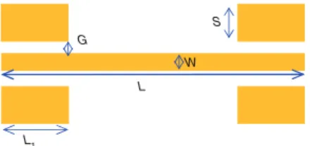
Topology of studied transitions and measurement conditions: The back-to-back GCPW-MS-GCPW transitions studied in this Letter are shown inFig. 1. The backside conductor used as ground plane for the micro-strip line is not patterned. The backside ground of the micromicro-strip and the coplanar ground are electrically short-circuited above a certain fre-quency owing to electromagnetic coupling between them. We measured the S-parameters of the realised transitions with a network analyser Agilent E8364B, the bandwidth of which covers the frequency range from 10 MHz to 50 GHz, using probes SuSSMicrotec 50A3N500GSG (bandwidth 40 GHz, pitch 500 mm and pad 30 mm) and a calibration substrate SussMicrotec CSR-4. L G W S L1
Fig. 1 Structure of studied back-to-back GCPW-MS-GCPW transitions
Simulation and measurement results with 254mm-thick substrates: The measured transitions are built with standard commercial substrates of three different permittivities for comparison: RO3006 (1r¼ 3, tand¼
0.0013 at 10 GHz), RO3006 (1r¼ 6.15, tand¼ 0.0025) and RO3010
(1r¼ 10.2, tand¼ 0.0035). They are metallised on both sides with
17 mm copper. The dimensions of the transitions are determined in order to have a 50 V characteristic impedance for both the MS and the GCPW sections. For example, with the substrate RO3003, the width W of the centre strip is 615 mm and the coplanar gap G is 185 mm. The length L of the microstrip line is 1 cm. The CPW pads are S ¼ 1 mm wide and L1¼ 1 mm long. All simulation results were
obtained with commercial electromagnetic analysis software for 3D microwave structures (HFSS) by taking into account the CPW probe dimensions used in the measurement. The calculated and the corre-sponding measured S-parameters are presented on the left and the right of Fig. 2, respectively. All the experimental and simulation results are in perfect agreement.
S21 , dB 0 –10 Ro3003 Ro3003 Ro3010 Ro3010 Ro3006 Ro3006 Ro3003 Ro3010 Ro3006 Ro3003 Ro3010 Ro3006 –20 –30 –40 –50 S21 , dB 0 –10 –20 –30 –40 –50 S11 , dB 0 –10 –20 –30 –40 –60 frequency, GHz frequency, GHz 0 5 10 15 20 25 30 35 40 0 5 10 15 20 25 30 35 40 –50 S11 , dB 0 –10 –20 –30 –40 –50
Fig. 2 Calculated (left) and measured (right) S-parameters of back-to-back GCPW-MS-GCPW transition on 254mm substrates with different permittivities
The high cutoff frequencies of the transitions due to the first parasitic resonance peak are, respectively, 20.6, 25 and 33.4 GHz for substrates of permittivities of 10.2, 6.15 and 3. Owing to the electromagnetic coup-ling between the backside conductor and the coplanar ground strips, the low cutoff frequency increases with decreasing permittivity, respect-ively, to 1.7, 2.4 and 4 GHz.
Discussion and ultra-broad bandwidth transition on thin BCB substrate on LRS: Low effective permittivity obtained by micromachining sub-strates allows us to obtain low-dispersive waveguides (quasi TEM approximation) and to realise CPW transmission lines with very high bandwidth without excessive dispersion and loss[9]. The main reason for improvement of the high cutoff frequency of GCPW-MS-GCPW transitions is that the wavelength is bigger in low-k substrate for a given frequency, so the parasitic resonance between the backside con-ductor and the coplanar ground strips takes place at higher frequencies. In addition, as for low effective permittivities a large part of the energy is propagating in air medium, so losses can be minimised. The parasitic resonance in the GCPW structure has been analysed by Raskin et al.
[7]. The electric field propagating in a GCPW line spreads into three modes owing to the backside conductor (seeFig. 3): microstrip mode (MS), coplanar mode (CPW) and coplanar microstrip mode (CPM). The CPM mode is excited between the backside conductor and the coplanar ground strips on the top of the substrate. It does not exist in a CPW structure without a backside conductor. The CPM mode causes the resonance peaks in the S21-parameter curve by diverting
input electromagnetic energy from the CPW mode. The thickness of the substrate has also an important influence on the CPM mode[10]. One can use a low-k and high resistivity material in thin film for sub-strate deposited on cheap LRS wafers to push the parasitic resonance to very high frequency, so the high cutoff frequency is increased. In addition the low cutoff frequency can also be improved owing to larger capacitive effect with shorter distance between the backside con-ductor and the coplanar ground strips.
CPM mode MS mode CPW
Fig. 3 Different propagation modes in GCPW structure
The commercial benzocyclobutene polymer (BCB), often used in microelectronic packaging and interconnection applications, is an excel-lent candidate as a substrate in thin film for GCPW-MS transition on LRS wafers, with its remarkable features: low-permittivity (1r¼ 2.65),
low loss tangent (tand¼ 0.0025), simple and cost-effective to deposit, varying thickness through the spinning-curing process, resistance to
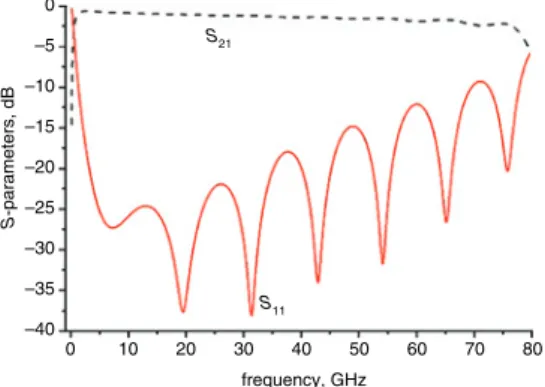
some chemical agents, etc.[4].Fig. 4shows the S-parameters obtained by simulation for a L ¼ 1 cm-long back-to-back GCPW-MS transition on h ¼ 8 mm-thick BCB polymer deposited on a metallised LRS wafer, the metal strips are in 4 mm aluminium, the width W of the centre strip is 19 mm and the coplanar gap G is 11 mm. The CPW pads are S ¼ 1 mm wide and L1¼ 1 mm long. The low and the high
cutoff frequencies are, respectively, 540 MHz and 77.4 GHz.
0 –5 S21 S11 –10 –15 –20 –25 S -parameters, dB –30 –35 –40 frequency, GHz 0 10 20 30 40 50 60 70 80
Fig. 4 Calculated S-parameters of back-to-back GCPW-MS-GCPW trans-ition on 8mm BCB substrate
Conclusions: We have presented in this Letter back-to-back GCPW-MS-GCPW via-free transitions on substrates of different permittivities. The low permittivity of the substrate permits pushing into higher fre-quencies parasitic resonance between the backside conductor and planar ground strips, so the bandwidth of the transitions is enlarged. The bandwidth could also be enlarged by using thin substrates but the requirement of 50 V characteristic impedance will limit the centre strip to only 9 mm with a h ¼ 8 mm-thick substrate of permittivity 1r¼ 6.15, which could worsen the adhesion of the metal strip to the
substrate, making difficult or even unusable the cost-effective chemical etching of the metal strips owing to the high aspect ratio. In addition, the narrower the centre strip is, the bigger is the ohm effect, and the larger is the negative slope of the S21-parameter curve, so band widening by
using thin substrates will be limited. Utilisation of low-permittivity and thin substrates permits reducing the negative slope and pushing the parasitic resonance frequency to enlarge the bandwidth of the GCPW-MS transitions, as is shown by the previous simulation results with BCB as substrate on LRS wafers. The bandwidth could go far beyond 60 GHz, which opens the perspectives of cost-effective circuits on LRS for 60 GHz wireless communication to undergo rapid expansion.
Acknowledgments: The authors thank Y. Mahe´ at IREENA for helpful discussion. The work was supported by the Region of Pays de la Loire and the ANR (French National Research Agency) through, respectively, the project Mattador/MILES and the project ModPol.
M. El-Gibari, D. Averty, C. Lupi, M. Brunet, H. Li and S. Toutain (Institut de Recherche en Electrotechnique et Electronique de Nantes Atlantique (IREENA), Universite´ de Nantes, Nantes cedex 3 44322, France)
E-mail: [email protected]
References
1 O, K.K., Cao, C., Seok, E.-Y., and Sankaran, S.: ‘100-200 GHz CMOS signal sources and detectors’. IEEE Compound Semiconductor Integrated Circuit Symp., 2007, Portland, USA, October 2007, pp. 1 – 4 2 Babakhani, A., Xiang, G., Komijani, A., Natarajan, A., and Hajimiri, A.: ‘A 77-GHz phased-array transceiver with on-chip antennas in silicon: receiver and antennas’, IEEE J. Solid-State Circuits, 2006, 41, pp. 2795 – 2806
3 Ponchak, G.E.: ‘RF transmission lines on silicon substrate’. 29th European Microwave Conf., Munich, Germany, October 1999 4 Wang, J.: ‘Polymer-based RF MEMS devices’, PhD thesis defended in
2007 at the University of Texas, USA
5 Haydl, W.H.: ‘Resonance phenomena and power loss in conductor-backed coplanar structures’, IEEE Microw. Guid. Wave Lett., 2000, 10, pp. 514 – 516
6 Xu, J., Sun, C., Xiong, B., and Luo, Y.: ‘Resonance suppression of grounded coplanar waveguide in submount for 40 Gb/s optoelectronic modules’, J. Infrared Millim. Terahertz Waves, 2009, 30, pp. 103 – 108
7 Raskin, J.-P., Gauthier, G., Kathei, L.P.B., and Rebeiz, G.M.: ‘Mode conversion at GCPW-to-microstrip-line transitions’, IEEE Trans. Microw. Theory Tech., 2000, 48, pp. 158 – 161
8 Michalah, R., Kuo, Y., Nash, F., Szep, A., Caffey, J., Payson, P., Haas, F., Mckeon, B., Cook, P., Brost, G., Luo, J., Jen, A., Dalton, L., and Steier, W.: ‘High speed AJL8/APC polymer modulator’, IEEE Photonics Technol. Lett., 2006, 18, pp. 1207 – 1209
9 Cheng, H.-J., Whitaker, J.F., Weller, T.M., and Katehi, L.P.B.: ‘Terahertz-bandwidth characteristics of coplanar transmission lines on low permittivity substrates’, IEEE Trans. Microw. Theory Tech., 1994, 42, pp. 2399 – 2406
10 El-Gibari, M., Averty, D., Lupi, C., Li, H.W., and Toutain, S.: ‘Ultra-wideband GCPW-MS-GCPW driven electrode for low-cost and wide range application electro-optic modulators’, Microw. Opt. Technol. Lett., 2010, 52, pp. 1078– 1082