Development in Utilizing Singlet Fission and
Triplet-Triplet Annihilation to Improve Solar Cell
Efficiency
byTony Chang-Chi Wu
Submitted to the Department of Electrical Engineering and Computer Science
in partial fulfillment of the requirements for the degree of
Doctor of Philosophy in Electrical Engineering and Computer Science at the
MASSACHUSETTS INSTITUTE OF TECHNOLOGY February 2018
@
Massachusetts Institute of Technology 2018. All rights reserved.Signature redacted
A u th or ... ...
Department of Eleeffical Engineering and Computer Science October 17, 2017
Certified by...S ...
Marc A Baldo Professor of Electrical Engineering and Computer Science Thesis Supervisor
Acepedby...Signature
redacted
Accepted by ... . . . .
U V Leslie A. Kolodziejski
Professor of Electrical Engineering and Computer Science Chair, Department Committee on Graduate Students
MASSACHUSETTS INSTITUTE
OF TECHNOLOGY- Cl
MAR
2 6 2018
Development in Utilizing Singlet Fission and Triplet-Triplet Annihilation to Improve Solar Cell Efficiency
by
Tony Chang-Chi Wu
Submitted to the Department of Electrical Engineering and Computer Science on October 17, 2017, in partial fulfillment of the
requirements for the degree of
Doctor of Philosophy in Electrical Engineering and Computer Science
Abstract
Our main energy source are burning fossil fuels. Solar energy is a clean, sustainable energy source that does not emit greenhouse gas that causes global warming. In this thesis, singlet fission and triplet-triplet annihilation would be discussed and studied to increase solar cell power conversion efficiency.
Singlet fission splits a singlet exciton into two lower energy triplet excitons. This energy down conversion is efficient and have shown near 200% triplet exciton yield. With energy down conversion, thermalization loss in solar cell could be reduced. We have shown singlet fission in tetracene, a suitable down conversion fission material to pair with silicon solar cell, up to 127% of internal quantum yield. To integrate tetracene as the energy down converter for silicon, we have demonstrated triplet exciton transfer from tetracene to silicon with WNx passivation. To show triplet exciton transfer, a spectrally resolved magnetic field effect measurement setup was designed and built.
We have also demonstrated a metal-free, solid state optical up conversion system. This is in contrast with most optical up conversion system that uses heavy metal for triplet generation and are limited to solution fabrication based on material restric-tions. The novel optical up conversion system provided cheaper material choices as well as better fabrication freedom and potentially longer device operation lifetime. Thesis Supervisor: Marc A Baldo
Acknowledgments
This thesis is done with support from many people in both academic colleagues and outside of research. The most important people to appreciate is my PhD advisor, professor Marc Baldo. He has guided me during my ups and downs, excitements and frustrations in research. He is also patient on my wild ideas and wisely point me to the right directions when I was lost in research. Thank you very much for all the enlightenment, Marc.
Many labmates in the SEE group have taught me and provided me great sugges-tions on research over the years. Thank you Carlijn, Jiye, Priya for teaching me on crystal growth and device fabrications. I also appreciate Nick, Shane, Phil, Matthias, Dan, Brian, Dong-Gwang, Jean Anne for discussing about research, science and oc-casionally sports. I would also like to specially thank Markus and Kurt for all the help on the difficult triplet transfer project. The project would not be possible with your help.
During my time at MIT, there has been ups and downs. I would like to thank my families and friends in both Taiwan and Boston. Thank you for the support all the years that push me through my PhD.
Contents
1 Introduction 23
2 Organic Semiconductors 25
2.1 Semiconductors . . . . 25
2.2 Semiconductors with Organic Molecules . . . . 27
2.2.1 Molecular Orbitals . . . . 28
2.3 Excited States in Organic Molecules . . . . 30
2.3.1 Spins in Excited states . . . . 30
2.3.2 Selection Rule . . . . 32
2.3.3 Exciton Transport . . . . 33
2.4 Organic Photovoltaics (OPV) . . . . 34
3 Singlet Fission and Triplet-Triplet Annihilation 37 3.1 Down Conversion and Up Conversion . . . . 37
3.1.1 Shockley-Queisser Limit . . . . 37
3.1.2 Overcoming the Limit . . . . 40
3.2 Physics of Singlet Fission and Triplet-Triplet Annihilation . . . . 43
3.2.1 Singlet Fission . . . . 43
3.2.2 Triplet-Triplet Annihilation . . . . 44
3.2.3 Magnetic Field Effect . . . . 45
3.3 Applications with Singlet Fission and Triplet-triplet Annihilation . . 49
3.3.1 Available SF and TTA Materials . . . . 49
3.3.3 Optical Up Conversion . . . .
4 Efficient Singlet Fission in Tetracene
4.1 Introduction . . . .
4.2 Device Structures and Fabrication . . . . 4.3 Magnetic Field Effect of Singlet Fission in Tetracene . . . . 4.3.1 Magnetic Field Effect Measurement . . . . 4.3.2 Magnetic Field Effect Measurement . . . . 4.4 Internal Quantum Efficiency . . . . 4.4.1 Optical Modeling . . . . 4.4.2 Optimal Device and Efficiency . . . . 4.5 Triplet Exciton Yield . . . . 4.5.1 Exciton Dynamics in Tetracene Devices . . . . 4.5.2 Magnetic Field Effect Dependencies on Exciton Diffusion Distance 4.5.3 Triplet Yield from Magnetic Field Effect . . . . 4.5.4 Singlet Exciton Dissociation Rates . . . . 4.6 Conclusion on Tetracene . . . .
5 Metal-Free Solid-State Optical Up Conversion 5.1 Introduction . . . .
5.2 Device Design . . . .
5.2.1 Thermally Activated Delayed Fluorescence . .
5.2.2 Structure and Fabrication . . . .
5.3 Triplet-Triplet Annihilation Up Conversion . . . .
5.3.1 Up Conversion Emission Spectrum . . . . 5.3.2 Magnetic Field Effect of TTA Up Conversion. 5.4 Up Conversion Efficiencies . . . .
5.4.1 Up Conversion Quantum Yield . . . .
5.4.2 Estimated Intensity for Up Conversion . . . .
5.4.3 Triplet Sensitizing Rate . . . .
5.5 C onclusion . . . . 51 53 53 54 55 55 57 58 59 60 61 61 64 65 66 67 69 . . . . . 69 . . . . . 70 . . . . . 70 . . . . . 71 . . . . . 72 . . . . . 72 . . . . . 73 . . . . . 74 . . . . . 74 . . . . . 76 . . . . . 77 . . . . . 78
6 Tetracene Triplet Excitons Transfer to Silicon 6.1 Introductions ... ...
6.2 Device Fabrication . . . . 6.3 Magnetic Field Effect of Silicon Photoluminescence . . . 6.3.1 Overlapping Emission Spectrum . . . .
6.3.2 Measurement Setup . . . .
6.3.3 Spectrally Resolved Magnetic Field Effect on WN Sam ple . . . . 6.3.4 Passivations without Triplet Transfer . . . . 6.4 Excitation Spectrum of Silicon Photoluminescence . . . . 6.4.1 D ifficulties . . . .
6.4.2 Measurement Setup . . . . 6.4.3 Excitation Spectrum of WNx Passivated Sample . 6.4.4 Model of Excitation Spectrum . . . .
6.5 Further Investigations of Triplet Transfer . . . .
6.5.1 Thickness Dependence of WNx . . . .
6.5.2 Doping Level . . . .
6.5.3 Red-Green MFE Experiment . . . .
6.6 Conclusion on Triplet Exciton Transfer . . . .
81 81 . . . . 82 . . . . 83 . . . . 84 . . . . 85 x Passivated . . . . 86 . . . . 88 . . . . 89 . . . . 90 . . . . 92 . . . . 93 . . . . 95 . . . . 97 . . . . 97 . . . . 98 . . . . 99 . . . . 101 7 Conclusion and Future Work
7.1 C onclusion . . . .
7.2 Future Road for the Project . . . .
A Publications
A.1 Singlet Fission and Triplet-Triplet Annihilation . . . . A.2 Thermally Activated Delayed Fluorescence . . . .
103 103 104 105 105 106
List of Figures
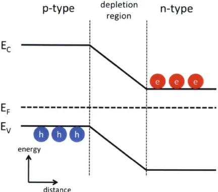
2-1 Conduction Band, Valence Band and p-n Junction. EC is the conduc-tion band energy; EV is the valence band energy; EF is the Fermi level. The Fermi level differences in p-type and n-type semiconductors causes the electrons to diffuse from n-type to p-type and holes to diffuse vice versa. After the Fermi levels balance, there will be a depletion region with built in potential between n-type and p-type materials. . . . . . 26
2-2 Simple Photovoltaic Diagram. Photovoltaics utilize the depletion re-gion to collect photocurrent. The semiconductor absorbs and an elec-tron are excited from the valence band. The carriers then diffuse to the junction and swept to the sides by the built-in potential. . . . . . 27 2-3 Organic semiconductor and semiconductor comparisons. On the left
are the energy levels for organic molecules; Highest Occupied Molec-ular Orbitals (HOMO) and Lowest Unoccupied MolecMolec-ular Orbitals
(LUMO). The electrons or holes in organic molecules are usually
local-ized and transport through hopping. In comparison, the right are the semiconductor conduction bands and valence bands, where electrons and holes move freely. . . . . 28
2-4 Spin of the Excited States. In a system of two identical particles, the energy states can be represented as one singlet state and three triplet states. ... ... 32
2-5 Singlet and Triplet Excitons in Organic Molecules. Due to selection
rules, singlet excitons are emissive while the triplet excitons are not emissive nor absorptive. The triplet excited state also has lower en-ergy compared to singlet state due to anti-symmetric wave functions. The anti-symmetric spatial wave function reduces the electron-electron repulsion energy in a molecules. . . . . 33
2-6 Exciton Transport. On the left is Dexter transfer
11],
where the elec-trons in donor LUMO jumps to the acceptor LUMO and the elecelec-trons from the accepter HOMO jumps to the donor, effectively moving the exciton. On the right is the F6rster resonance energy transfer (FRET)[2].
F6rster transfer is an energy transfer through a non-radiative dipole-dipole coupling, requiring the molecule states to be emissive and absorptive. . . . . 342-7 Schematics for Organic Photovoltaic. The HOMO LUMO energy
lev-els of donor and acceptor in an organic photovoltaic are plotted. The excitons created in the material can diffuse to the donor-acceptor inter-face and transfer to the charge-transfer state. Once the charge-transfer state are formed, the excitons then dissociate into electrons on acceptor material and holes on donor. The carriers transport to the electrodes and get collected as photocurrent. . . . . 35
3-1 Main Energy Losses in the Shockley-Queisser Limit. The first main
loss is from non-absorption. For incident photon energies Eh, that are
lower than the band gap energy Eg, the photons are not absorbed. The second loss is from thermalization. For photons with energy Eh, higher than Eg, the photons can be absorbed, creating electrons and holes. However, the carriers will relax to the band gap energy, losing excess energy. An additional loss comes from carrier extraction. Practically, it is impossible to extract the carriers with the potential difference of the band gap. The solar cell will operate at a voltage lower than the
E9. This depends on multiple factors such as temperature and material
radiative efficiency. . . . . 38
3-2 Shockley-Queisser Limit. (a) Detailed balance limit for single junction
solar cells. Due to the trade off, a single junction solar cell has an optimum band gap energy E. that has maximum power conversion efficiency (PCE). The maximum PCE is 33.7% for Eg = 1.34 eV. As a comparison, silicon solar cell has a maximum PCE of 33.4% Eg =
1.12eV.
13]
(b) Efficiency losses for a single junction solar cell withEg = 1.34eV. From the solar spectrum and its contribution to PCE,
there is 29.7% loss due to photons that are not absorbed, 23.3% loss from thermalization and 13.3% from extraction loss. This leaves 33.7% of available energy
[3].
The solar energy spectrum is from NREL[4].
393-3 Down Conversion Efficiency Spectrum and Maximum PCE Curve. (a)
With down conversion, the solar cell could utilize about twice more photocurrent where the spectrum Eh, > 2Eg. Due to higher pho-tocurrent in the device, the extraction efficiency is also slightly higher, as the blue area is marginally larger in range, which can be seen in
2Eg > Ehv > Eg. (b) The improved PCE for different band gap
en-ergy. As expected, the maximum PCE 41.9% is higher than single junction solar cell maximum PCE 33.7%. Also, optimum band gap Eg 0.95eV is lower than Eg = 1.34eV to recycle more energy in the blue
region . . . . . 4 1 3-4 Up Conversion Efficiency Spectrum and Maximum PCE Curve. (a)
With up conversion, the solar cell could utilize the spectrum in Eg >
Ehv > -. Due to higher photocurrent in the device, the extraction
efficiency is also slightly higher. (b) The improved PCE for different band gap energies with up conversion. As expected, the maximum PCE 50.8% is higher than single junction solar cell maximum PCE 33.7%. The optimum band gap Eg = 1.87eV is higher than E =- 1.34eV to collect more energy in the red region. . . . . 42
3-5 PCE Limit of Using Different Energy Conversion Schemes. The PCE
limit with down+up conversion is plotted with down conversion, up conversion and a single junction solar cell. As expected, utilizing both down and up conversion increases the maximum PCE (51.2%). . . . 43
3-6 Schematic of Singlet Fission. When the triplet state energy ET is about
half of the singlet state energy Es, singlet excitons in organic material may undergo fission which splits them into two triplet excitons. Singlet exciton first transition into a triplet-triplet (TT) pair state. The TT pair state can then dissociate into two triplet excitons, effectively doing energy down conversion. This process can be efficient because the direct transition from singlet to triplet is not allowed or very inefficient based on selection rule 2.16. . . . . 44
3-7 Schematic of Triplet-triplet Annihilation. Triplet-triplet annihilation (TTA) is the reverse process of singlet fission (2ET - Es). Two triplet
excitons may diffuse and collide, forming a TT pair state. The TT pair state could then transition into a singlet exciton, which can then be col-lected through emission or charge-transfer states. TTA is a mechanism that does energy up conversion. . . . . 45
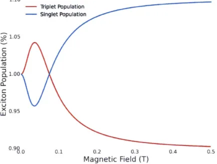
3-8 Magnetic Field Effect of Singlet Fission Rate from Equation 3.7. The fission rate first increases due to more TT pair states (from 3 up to 6) with spin 0 characteristics. It then decreased to 2 states with spin 0 characteristics, slowing the fission rate. The constants D = -56t100e
and E = 350 1 300e used in equation 3.2 is from 15]. . . . . 47
3-9 Singlet and Triplet Exciton Population under Magnetic Field in a Sin-glet Fission Material. The triplet population MFE in a fission material follows the fission rate because slower fission rates result in less triplet excitons. The singlet population MFE is opposite where a slower fission rate result in more singlet excitons. . . . . 48
3-10 Common Singlet Fission and Triplet-Triplet Annihilation Molecules.
Left, the top two molecules are tetracene and pentacene, oligoacenes with 4 and 5 phenyl rings. These two are well studied and have good singlet fission efficiencies. The bottom left molecule is 9,10-dicyanoanthracene, an efficient blue fluorescence emitter with triplet-triplet annihilation. The molecule on the right is rubrene, which is a tetracene derivative that also does TTA. . . . . 50 3-11 Device Architecture of Pentacene OPV and over 100% EQE. (result
from 16], consent from authors.) (A) Chemical structures and archi-tecture of the pentacene solar cell with the thickness of each layer in nanometers and energy levels of the LUMO and HOMO. (B) Over
100% external quantum efficiency of devices measured with light
inci-dent at 100 from normal with an external mirror reflecting the residual
4-1 Device Structure and Band Diagram of Tetracene Photovoltaics and Photodetectors. For photodetector structures, tetracene/C60 layers are
fabricated in multiple pairs of layers. Thicknesses are in nanometers and band energy levels are in electron volts. m-MTDATA is introduced as a triplet exciton blocking layer to increase exciton dissociation at the donor/acceptor interface. The structures of the molecules are also shown for m-MTDATA, tetracene andCC0 . . . . . 54 4-2 Magnetic Field Effect Measurement Setup. This is the setup to
mea-sure the magnetic field effect (MFE) of the fluorescence from tetracene film or photocurrent from tetracene device. To measure small signal changes under 0.1%, a lock-in amplifier (SR830) is used to measure fluorescence or photocurrent. ... ... 56
4-3 Magnetic Field Effect Analysis. To detect the small magnetic field effect changes, the external magnetic fields are applied in on to off cycles. This method allows us to reduce the effects of signal drift such as degradation or sample annealing. The signal curve (red) is fitted to a polynomial function of time x(t) with a Ax change when magnetic field is applied (fitting curve: light red). Ax will be the magnetic field effect change. The magnetic field strength measured is plotted in blue. The measured signal is the photocurrent of a 20nm Tetracene/30nm
C6 0 device. . . . . 57
4-4 Magnetic Field Effect (MFE) of Tetracene. Fluorescence changes of tetracene crystals (green square) and thin film solar cells (red triangle) as a function of magnetic field. The photocurrent of a 30nm thick tetracene solar cell displays the opposite sign to the measured changes in fluorescence. Both fluorescence of MFE trends match well and follow the trend of the singlet exciton population. The photocurrent MFE matches to the triplet exciton populations. . . . . 58
4-5 Modified Exciton Kinetic Model for Tetracene Devices. The modified kinetic model, compared to pentacene model in Congreve et al.
16],
includes the fluorescence rate from singlet excitons. . . . . 59
4-6 Measuring Refractive Index. The sample is a 15nm of tetracene on glass substrate. The transmission and reflectance (TR) of a sample are measured under excitation with traverse magnetic (TM) mode and traverse electric (TE) modes (green). With transfer matrix
17],
the n and k of the material are then fitted to minimized the total errors (red). 60 4-7 Obtaining Internal Quantum Efficiency of Devices. The dashed blueand red curves are estimated tetracene and C60 EQE contributions
obtained by multiplying the absorption spectrum by a factor. The factor will be the IQE of the layer. The simulated photocurrent is a black dashed line and the measured EQE curve is a black solid line. The device is a photovoltaic cell with tetracene layer thickness x = 25n m . . . . 6 1
4-8 Internal Quantum Efficiency. The IQE of photovoltaic devices as a function of the thickness, x, of the constituent tetracene layer. From the data, a maximum IQE of 127 18% is achieved in a tetracene
device with x - 25nm. The pentacene data are compared (data from Congreve et al.
16]).
The pentacene devices have a higher IQE of 160% and also show a faster fission rate with higher IQE in thin pentacene layers. ... ... 624-9 Magnetic Field Effects with Varying Exciton Diffusion Distance. The MFE of tetracene fluorescence change 6F and photocurrent change 6, are plotted as a function of the maximum exciton diffusion length in the device. The tetracene fluorescence MFE are measured in the corre-sponding sample with same thicknesses. The MFE of the photocurrent changes are corrected with the IQE ratio of tetracene and C60.
Pen-tacene 6, are also plotted for comparison, showing again a faster fission rate. ... ... ... 64
4-10 Triplet Exciton Yields in Tetracene and Pentacene. The red squares represent the triplet exciton yield approximated by the 6F-Only-approach. Orange triangles represent the full calculation of triplet yield based on both 6F and the photocurrent change 6r in figure 4-9. The data showed a maximum of 192% triplet yield in thick tetracene layers. As a com-parison, pentacene reach 200% triplet yields. . . . . 65
4-11 Singlet Dissociation Rates. Singlet dissociation rate Xs from modeling fluorescence change plotted with different exciton traveling length. The Xs of tetracene:C60 blend in Yost et al.
181
was included as a comparisonwith our m ethod. . . . . 67
5-1 Schematic of Thermally Activated Delayed Fluorescence. In OLEDs,
an exciton formed by electron and hole recombination creates 25% singlet excitons and 75% triplet excitons. In thermally activated de-layed fluorescence (TADF), the energy gap between singlet and triplet state are designed to be small (< 0.1eV). This increases the thermally induced inter-system crossing from triplet excitons back to singlet ex-citons and then fluoresce. . . . . 70
5-2 TADF-TTA Up Conversion Schematics and Device Structure. (a) The
low energy excitation photons are first absorbed by the TADF molecule 4CzTPN-Ph, creating singlet excitons. Due to strong inter-system crossing in TADF, the singlet excitons form triplet excitons. A triplet exciton on 4CzTPN-Ph can then Dexter transfer to the triplet on DPA and up convert to a singlet exciton via triplet-triplet annihilation. High energy photons then emit from singlet excitons. (b) Our devices are simple bilayer thin films with 50nm of DPA and 20 nm of 4CzTPN-Ph. The HOMO and LUMO energies of DPA are 5.81eV and 2.87eV
191,
where the energy levels of 4CzTPN-Ph are 5.9eV and 4.0eV 1101. . . 725-3 Optical Up Conversion Spectrum. The spectrum shows emission from three different devices (red, green, blue curve) with 532nm laser ex-citation. The red curve is DPA + 4CzTPN-Ph device emission, where there are significant emission between 400nm - 500nm comparing to emission spectrum of 4CzTPN-Ph (green) and DPA (blue) only. This is attributed to up conversion emission. The yellow dotted curve shows the DPA fluorescence spectrum as a comparison. . . . . 73
5-4 Up Conversion PL Change under Magnetic Field. The magnetic field
effect shows up conversion rate correlates to triplet-triplet annihilation rate under magnetic field. . . . . 74
5-5 Relation Between Up Converted Photoluminescence and Excitation Intensity. We show the relationship with trend PL oc J1.28. . . . . . 76
5-6 4CzTPN-Ph Dexter Transfer to DPA. The red and blue curve represent the triplet delayed fluorescence rate of 4CzTPN-Ph. With DPA, the transient lifetime of 4CzTPN-Ph decreases from 1.72ps to 1.56ps. The decrease is due to triplet exciton quenching with DPA. We show that the in our system, 9.1% of triplets in 4CzTPN-Ph are transferred to DPA. ... ... 78
6-1 Schematics of Tetracene Down Converter for Silicon. For photon en-ergy Eh, > 2.3eV, the photons are absorbed by tetracene and split into to lower energy triplet excitons ET = 1.25eV. If the triplet excitons then transfer to silicon and are collected as charges, then effectively this down converter collects more photocurrent per absorbed photon in the blue. The silicon material by itself still absorb photons from Eh, = 1.12 ~ 2.3eV . . . . . 82
6-2 Structures and Fabrication of Tetracene/Silicon Devices. The silicon
substrate are cleaned with standard RCA cleaning 111]. We can pas-sivate the surface with H-termination with an HF etch (1% HF). The interface is then built from different material using atomic layer de-position (ALD). Finally, tetracene is deposited on the sample through thermal evaporation in vacuum chamber (2 x 10⁻⁶ torr). . . . . 83 6-3 Emission Spectrum of a Tetracene/Silicon Device. The emission peak
around 1100nm is from silicon, which matches to the silicon only PL spectrum in dashed green curve. The tetracene emission overlaps with silicon, shown in dashed red curve. The spectrometer response de-creases for wavelengths below 950nm. . . . . 84 6-4 Spectrally Resolved Magnetic Field Effect Measurement Setup. This
is the setup to measure the MFE of the silicon emission spectrum. The infrared spectrometer is a nitrogen cooled InGaAs spectrometer from Princeton Instrument. An external trigger (using a Keithley 2400) is used to control the spectrometer to acquire the spectrum through program . . . . . 85 6-5 Spectrally Resolved MFE of a WNx Passivated Sample. (a) The
spec-tral difference of silicon PL between the on and off magnetic field. The silicon peak difference (~ 1100nm) is negative a large magnetic fields
(B > 0.05T). The tetracene emission difference (~ 950nm) shows an
increase with large magnetic field. (b) MFE change plotted as percent-age change relative to emission intensity. . . . . 86 6-6 MFE for Different Spectral Range. The MFE of the silicon PL peak
(1100-1150nm) is plotted in blue, showing a MFE trend similar to the triplet population MFE. This indicates that triplet excitons transfer and inject into silicon for a WNx passivated sample. The MFE of the spectrum for tetracene emission (900-950nm) is plotted in red and has a similar trend to the singlet population MFE. . . . . 87
6-7 MFE of H-passivated/Tetracene Sample. (a) The spectral difference between and and off states of the magnetic field. Both the silicon PL and tetracene emission differences showed a positive MFE. (b) The MFE of tetracene emission (red) and peak MFE fo silicon PL (blue) are shown. Both MFE have similar trends to the singlet exciton pop-ulation. This indicates at best inefficient triplet exciton transfer from tetracene to silicon. . . . . 88
6-8 MFE of Silicon PL Peak with Different Passivation. The MFE of silicon
PL are measured with WNx and H-terminated passivation. Along with these, SiOx, HfOX, MoOx passivation are also measured. Among these materials, only WNx showed triplet MFE, indicating triplet exciton transfer. . . . . 89 6-9 Variable Laser Source Intensity Changes. The Peak to peak intensity
differences in our variable laser source (SuperK from NKT Photonics) are up to a factor of 10. . . . . 91 6-10 Measure Silicon PLQY with Different Excitation Wavelengths. The
silicon PLQY decreases with shorter excitation wavelengths. . . . . . 92 6-11 Excitation Spectrum Measurement Setup. To be able to measure the
silicon PL, the infrared spectrometer is used to measure the emission spectrum. The variable laser source is a SuperK from NKT Photonics which allows different excitation wavelengths. The laser intensity is then measured and stabilized through a photodetector with a lock-in amplifier. The samples are held on a optical translation stage from Thorlabs that allows us to measure at different locations on the sample. 93
6-12 Silicon Emission of WNx Passivated Samples. The blue circles are the
silicon emission intensities of a sample with 20nm tetracene. The red circles are the emission of a plain sample. The sample has a same device structure in section 6.3.3. Multiple measurements are done for each excitation wavelengths. . . . . 94
6-13 Excitation Spectrum of WNx Passivated Samples. The relative
excita-tion signal is calculated by averaging the emission at each wavelength in figure 6-12 and dividing the PL with tetracene to the PL without. The relative PL is then normalized with the values from > 600nm. An increase in the excitation spectrum is measured at the wavelengths where tetracene absorbs A < 540nm. The error bars are also calcu-lated and are larger in the tetracene absorption range due to errors introduced during spectrum decomposition. . . . . 95
6-14 Excitation Spectrum with Modeling. The blue circles are the excitation spectrum from a WNx passivated sample, where the red circles are measured from the H-passivated sample. The dashed lines are the fitted model for respective excitation spectra. . . . . 96 6-15 MFE Dependencies on WNx Passivation Thicknesses. The MFE for
B > O.4T with different WNx passivation thickness are measured. The
MFE increases with several cycles for WNx and decreases at thick layers. ... ... 98 6-16 MFE of Silicon PL with Different Doping Levels. The large magnetic
field (B > O.4T) MFE are measured with different doping levels of
silicon wafers. All of the device have WNx passiavation with 20nm of tetracene deposited on top. . . . . 99
Chapter 1
Introduction
The first two chapters will provide introduction and the background for the results in this thesis. Chapter 2 will briefly introduce the physics organic semiconductors and its usage in organic photovoltaics (OPV). In chapter 3, 1 will discuss the background on singlet fission and triplet-triplet annihilation 112, 13, 14], which is an essential part of this thesis.
From chapters 4 to 6, I will be showing my results in singlet fission and triplet-triplet annihilation. In chapter 4, I will characterize the efficiencies of singlet fission in tetracene. The realization of efficient fission in tetracene extended to the project on demonstrating triplet exciton transfer from tetracene to silicon in chapter 6. These results are the first steps for creating a down converter for silicon solar cells. In chapter 5, I will show a novel optical up conversion device structure that does not require solution processing and heavy metals.
Chapter 2
Organic Semiconductors
2.1
Semiconductors
Semiconductor materials have conductivities in between a conductor and an insu-lator. The conducting property is due to the reason that semiconductor material has smaller energy bandgap compared to insulators, which is the gap between con-duction band (mobile electrons) and valence band (mobile holes, vacant electrons). Conductivity in a semiconductor can be altered by introducing impurities (doping) or gating with applied electric field. Doping and gating can change the conductivity and majority carrier type in the material, where n-type indicates the material con-taining mostly free electrons and p-types concon-taining mostly free holes. By placing p-type and n-type materials together, a p-n junction is created. p-n junctions are the fundamental elements for semiconductor devices, which includes integrated circuits (in CPU), photovoltaics and light-emitting diodes (LEDs).
In figure 2-1, the energy levels and band structures of a p-n junction is plotted. The Fermi level is the energy level where the electrons in the material are filled up to, or more precisely, there will be 50% chance of electrons occupying the level at thermodynamic equilibrium. In a system where charges are free to move, the energy bands will bend until Fermi levels are in equilibrium. The n-type material has a higher Fermi level (closer to the conduction band, more free electrons) compared to p-type (closer to the valence band, more free holes). In a p-n junction, this creates
p-type
depletionn-type
regionEF
EFE
energy distanceFigure 2-1: Conduction Band, Valence Band and p-n Junction. Ec is the conduction band energy; Ev is the valence band energy; EF is the Fermi level. The Fermi level differences in p-type and n-type semiconductors causes the electrons to diffuse from n-type to p-type and holes to diffuse vice versa. After the Fermi levels balance, there will be a depletion region with built in potential between n-type and p-type materials.
a Fermi level difference, causing the electrons to diffuse from n-type to p-type and holes to diffuse vice versa. After the Fermi levels balance, there will be a depletion region with a built-in potential between n-type and p-type materials. This creates interesting properties for electrical devices. For example, under forward bias (using the figure as an example, the left side is connected to a higher voltage than the right), the depletion region will decrease and eventually thin enough for the electrons and holes to tunnel across the junction and recombine. There is a rapid current increase when the forward bias is larger than a threshold voltage. However, if the p-n junction is reversed biased, the depletion region will increase and minimal current will flow through.
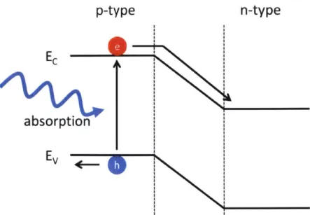
Photovoltaics utilize the depletion region to collect photocurrent. In figure 2-2, the photon absorbed may excite an electron from the valence band. The carriers
E
absorption
EV
Figure 2-2: Simple Photovoltaic Diagram. Photovoltaics utilize the depletion region to collect photocurrent. The semiconductor absorbs and an electron are excited from the valence band. The carriers then diffuse to the junction and swept to the sides by the built-in potential.
can then diffuse to the junction and split by the built-in potential at the depletion region. The carriers diffusion lengths in the material are important parameters in the determination of the overall solar cell power conversion efficiency.
2.2
Semiconductors with Organic Molecules
Organic semiconductors are based on organic molecules or polymers which mainly consist of carbon, hydrogen and occasionally oxygen, nitrogen, sulfur, etc. This is in contrast to semiconductors where the crystals are based on atoms. In the crystals, the orbitals of the valence electrons of the atoms overlap. For a two atoms system, the overlapped orbitals splits into a higher and lower energy molecular orbitals. With
N multiple atoms, the molecular orbitals splits into N higher energy levels and N
lower energy levels. Due to many atoms in a semiconductor material, the high and low energy levels could be viewed as conduction bands and valence bands. Organic molecule's valence orbitals are typically more localized because molecules are bound together in a solid by Van der Waals force. Hence, some properties in organic
conductors should be treated differently. 2.2.1 Molecular Orbitals energy LUMO --- conduction band HOMO
Lvalence
-+V bandFigure 2-3: Organic semiconductor and semiconductor comparisons. On the left are the energy levels for organic molecules; Highest Occupied Molecular Orbitals (HOMO) and Lowest Unoccupied Molecular Orbitals (LUMO). The electrons or holes in organic molecules are usually localized and transport through hopping. In comparison, the right are the semiconductor conduction bands and valence bands, where electrons and holes move freely.
In an organic molecule, the energy levels of interest are the Highest Occupied Molecular Orbitals (HOMO) and the Lowest Unoccupied Molecular Orbitals (LUMO). HOMO levels are the highest electron energies for molecules in ground states, and the
LUMO levels are for additional electrons to occupy. These energy levels are similar
to the valence bands and conduction bands. However, organic molecular crystals are formed from the weak interaction of Van der Waals bonds. Thus, the HOMO and
LUMO energy levels are treated as localized in the molecules instead of viewing them
as delocalized conduction and valence bands. Therefore, the electrons or holes in organic molecules move in the material through hopping instead of conduction.
To understand how the electrons occupy energy levels, we would need to under-stand the states of identical particles. In quantum mechanics, a particle state could be represented as In) that includes spacial, angular momentum, spins, etc. We first start from understanding a simple two particle system, which can then be extended
to multiple particles system. The state of two particle system can be expressed as 10(ni, n2)) where the ni represent the states for particle 1 and n2 for particle 2.
Assuming a swapping operator P that switches the states of particle 1 and 2, then Pl(ni, n2)) = 10(n2, ni)). For two states to be physically equivalent under mea-surements, the wavefunctions should only be different by a factor of complex number
|0) = alo). Therefore, the states of identical two particle system should satisfy,
PI1r(ni, n2)) = a 1(ni, n2)). (2.1)
From equation 2.1, the simple expression of two particle system 10(ni, 12)) =
ni) 1n2) cannot describe an identical two particle system because I n2)1ni) # a Ini)In2) for any states n. To express an identical two particle system with ni and n2, we assume the state 1') is the linear combination of the possible joint states, then it can be expressed as,
10(ni, n2)) = ani)|n2) + bIn2)Ini). (2.2)
From equations 2.1 and 2.2,
an2)1n) + bn11)|n2) = a(alni)122) + bln2)|n)) (2.3)
>aa = b, ab = a. (2.4)
From solving the simple relations, a = 1. a and b can then be solved for respective
a with normalization constraints. With the constants, the states to describe identical two particle systems is expressed as,
1
IV)(ni, n2)+) = (In,) 12) + 1n2)1In)) , (2.5)
1 (ni, n2)) (In,)11n2) - 1n2) In,)) . (2.6)
Particles in identical particles systems that are symmetric, described by 2.5, are called Bosons, where as the particles that are anti-symmetrical, described by 2.6, are Fermions. One big difference between Bosons and Fermions is the symmetry.
In equation 2.6, ni cannot equal n2 for the Fermions or else (k_ Ik-) = 0. Hence,
the Pauli exclusion principle indicates that no two Fermions may occupy the same state. However, Bosons are not constrained by the Pauli exclusion principle. Common Fermions include electrons or protons, where photons are Bosons.
The state of an electron can be represented as
In) =
l0(x)x),
(2.7)where O(x) is the spacial wave function and X is the spin function. Thus, for electrons to occupy the same energy level 01 = '2, the spin function of the electrons must be
different due to the Pauli exclusion principle. Because the electrons only have spins 2, only two electrons may occupy the same energy level and the spins of those electrons must be - and -1. 2 2 Therefore in the ground state of an organic molecule, the HOMO energy level has two electrons with spins 1 and -1. The spin eigenstates calculations are based on Quantum Mechanics Books written by Shankar 1151 and
Sakurai 1161.
2.3
Excited States in Organic Molecules
Excitons are electron hole pairs in semiconductors. Organic materials have low di-electric constants in organic materials. Thus, the excitons usually have large binding energy, typically on the order of 0.5eV 117] compared to excitons in semiconductors. Also, due to weak interactions between the molecules, the excitons are localized to one or few molecules. Based on the reasons, the excitons in organic semiconductors are best treated as localized excited states.
2.3.1
Spins in Excited states
The organic molecule may absorb a photon and promote an electron from HOMO energy level to LUMO energy level. Based on the equation 2.7 in section 2.2.1, since the two electrons does not have the same spatial wave functions, the excited states
can have 4 possible spin combinations: I Tt) m
14S)
= rmsi I44) =Irms1 I 44) ImSi 1 1 = , 2 = - ) 2 2 1 1 = , m .2 = 2 2 1 1 2 2 1 2 = 2' s 2)In the equations above, m, is the secondary spin quantum number of an electron that describes the spin projected in the z direction. It could be 1 for electrons. The total spin of the electron is s However, the states in the above equations are
not eigenvectors for S2 (operator that measures total spin). The eigenvectors of the
excited states that satisfies both S2 and Sz are then calculated and expressed as,
1 Is =0, m = 0)=
(1
14)-
-1))
is = 1,ms = 1) = Tt) 1 is =11, - -1) = I 'W). (2.12) (2.13) (2.14) (2.15)The eigenstates are categorized into two spin states, one singlet states with total spin s = 0 and three triplet states with spin s = 1. These are the eigenstates for the
excited states. The ground state can only be a singlet state due to the Pauli exclusion principle. Singlet and triplet configuration of the excited state are plotted in figure 2-4.
(2.8) (2.9)
(2.10) (2.11)
energy
LUMO +
+
HOMO +
++
+
++
s=1 s=1 s=1 s=O
m5=1 m,=O m=-1 ms=O
Triplet states Singlet state
Figure 2-4: Spin of the Excited States. In a system of two identical particles, the energy states can be represented as one singlet state and three triplet states.
2.3.2 Selection Rule
From the equations 2.12 - 2.15, the singlet states are anti-symmetric under particle
exchange while the triplet excitons are symmetric. This is important to determine whether if a electric dipole transition is allowed. Under Fermi golden rule, the tran-sition between an excited state and the singlet ground state can be written as,
(kexL tedIdkground) = (xexcitedXground) ()ezcitedIdV) ground) (2.16)
where d is the dipole transition moment. From the first term of the right hand side,
the spin transitions can only be non-zero if the spin wave functions are the same. If one is a triplet state and the other is singlet state, the integral would be zero due to anti-symmetry of the product. Since the ground state of a molecule is typically a singlet, only singlet excited states can emit photons or be created from ground states through absorbing photons. The triplet states are usually inaccessible and called dark state due to their forbidden transitions.
From equation 2.6, we know that the two Fermions are anti-symmetric, thus the spatial wave function of a singlet state is symmetric while the triplet state's spatial
singlet . state triplet
emission..-state disallowed groundFigure 2-5: Singlet and Triplet Excitons in Organic Molecules. Due to selection rules, singlet excitons are emissive while the triplet excitons are not emissive nor absorptive. The triplet excited state also has lower energy compared to singlet state due to anti-symmetric wave functions. The anti-anti-symmetric spatial wave function reduces the electron-electron repulsion energy in a molecules.
wave function is anti-symmetric. The anti-symmetry of the triplet state spatial wave function reduces the electron-electron repulsion energy in a molecules, reducing its energy compared to the singlet excited states.
2.3.3 Exciton Transport
Excitons are strongly localized within the organic semiconductor materials. In figure
2-6, we show two possible ways for an exciton to transport in a material. The first is
Fbrster resonance energy transfer (FRET) [2]. Fdrster transfer is an energy transfer through a non-radiative dipole-dipole coupling. This transfer requires the molecule states to be emissive and absorptive. Thus, the singlet excitons may transport through Fbrster transfers while triplets generally do not. Another transport mechanism is Dexter transfer [1], where an electron on the donor LUMO jumps to the acceptor
LUMO and the electron from the acceptor HOMO simultaneously jumps to the donor,
effectively moving the exciton. This does not require the molecular states to be radiative. The mechanism, however, requires the wave functions between the organic molecules to overlap for efficient transfer.
energy electron dipole-dipole exchange coupling LUMO I t HOMO
Dexter Transfer
F6rster Transfer
Figure 2-6: Exciton Transport. On the left is Dexter transfer
11],
where the electrons in donor LUMO jumps to the acceptor LUMO and the electrons from the accepter HOMO jumps to the donor, effectively moving the exciton. On the right is the F6rster resonance energy transfer (FRET)12].
F6rster transfer is an energy transfer through a non-radiative dipole-dipole coupling, requiring the molecule states to be emissive and absorptive.2.4
Organic Photovoltaics (OPV)
Organic photovoltaics are solar cells where the materials are organic molecules instead of semiconductors. The basic device structure of an organic photovoltaic consists of a donor and acceptor material where the energies levels EDHOMO > EA,HOMO
and ED,LUMO > EA,LUMO (D = donor energies, A = acceptor energies). Charge
transfer states, where the electrons and holes are on different molecules, are formed at the donor-acceptor interface. The energy of the charge transfer state ECT
-EA,LUMO -
EDHOMO-Photons absorbed in the organic material can create excitons. The excitons then propagate to donor-acceptor interface and form the charge-transfer state. Once the charge-transfer state is formed, the excitons may then dissociate into electrons on the acceptor material and holes on the donor. The carriers can then diffuse to the electrodes and get collected as photocurrent. Figure 2-7 is a simple OPV schematic.
The operation of an OPV is similar to a semiconductor solar cell. The organic donor materials are similar to p-type materials whereas the acceptors are n-type
* I dn
donor
I0cathode
acceptor
Figure 2-7: Schematics for Organic Photovoltaic. The HOMO LUMO energy levels of donor and acceptor in an organic photovoltaic are plotted. The excitons created in the material can diffuse to the donor-acceptor interface and transfer to the charge-transfer state. Once the charge-charge-transfer state are formed, the excitons then dissociate into electrons on acceptor material and holes on donor. The carriers transport to the electrodes and get collected as photocurrent.
materials. Recently, the power conversion efficiency in a OPV have reached 11.5%
118]. In comparison, silicon solar cell have reached 26% power conversion efficiency
1191.
OPV usually suffers from low fill factors (below 70%) and short device lifetime. In chapter 3, I will discuss more about energy down conversion and up conversion mechanisms called singlet fission and triplet-triplet annihilation that occur in organic semiconductors. The chapter will show the possibility of utilizing these mechanisms to increase solar cell efficiencies.energy
/I
Chapter 3
Singlet Fission and Triplet-Triplet
Annihilation
As mentioned in chapter 2, the current silicon solar cell power conversion efficiency record is 26.0% 1191 and the record for organic photovoltaics is 11.5% 1181. The fundamental limits for solar cell power conversion efficiency (PCE) will be discussed in this section. In this section, I will show some of the mechanisms that could overcome these limits.
3.1
Down Conversion and Up Conversion
Down converison and up conversion are some mechansims that may overcome the
PCE limit that will be studied in this thesis. To understand the limits, in this
section I will show the theoretical limits of a single junction solar cells imposed by the Shockley-Queisser limit [3].
3.1.1
Shockley-Queisser Limit
Energy losses in a single-junction solar cell are shown in figure 3-1 based on the Shockley-Queisser limit
131.
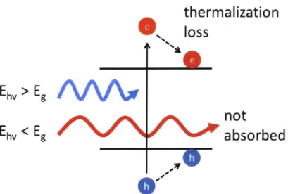
The first main loss is from non-absorption. For incident photon energies Ehv that are lower than the band gap energy Eg, the photons are notthermalization
0%,
loss
Eh,>Eg
not
Ehv <Eg
absorbed
00
0 0'Figure 3-1: Main Energy Losses in the Shockley-Queisser Limit. The first main loss is from non-absorption. For incident photon energies Eh, that are lower than the band gap energy Eg, the photons are not absorbed. The second loss is from thermalization. For photons with energy Eh, higher than Eg, the photons can be absorbed, creating electrons and holes. However, the carriers will relax to the band gap energy, losing excess energy. An additional loss comes from carrier extraction. Practically, it is impossible to extract the carriers with the potential difference of the band gap. The solar cell will operate at a voltage lower than the E. This depends on multiple factors such as temperature and material radiative efficiency.
absorbed. The second loss is from thermalization. For photons of energy Eh, higher than Eg, the photons can be absorbed, creating electrons and holes. However, the carriers will relax to the band gap energy, losing their excess energy. An additional loss comes from carrier extraction. Practically, it is impossible to extract the carriers with the potential difference of the band gap. The solar cell will operate at a voltage lower than the E, where e is the charge of an electron. This depends on multiple factors such as temperature and material radiative efficiency. Decreasing band gap energy Eg increases photon absorption but also increases thermalization losses. The trade off between thermalization and absorption decides the optimized efficiency band gap.
In figure 3-2a, the PCE limit for each band gap energy Eg is calculated. Based on the losses shown in figure 3-1, there will be an optimal band gap energy Eg that has a maximum PCE. The maximum PCE for a single junction solar cell is 33.7%
35 Si: Eg-1.12eV PCE-33.4% Eg=1.34eV - PCE=33.7% ~e30 U 25 W 20 C 0 IA 15 0 U 10 05 8.0 0.5 1.0 1.5 2.0 2.5 3.0 3.5 4.0 Eg (eV)
(a) Efficiency Losses for Maximum PCE Singlet Junction Solar Cell.
1.8 1.6 -1.4 E C 1.2 E 1.0 C 0,8 -0.6 0.4 0.2 0.0 4.5 500 in(b) Maximum Cells. Eg - 1.12eV
M 19.2% Not Absorbed Loss
M 31.7% Thermalization Loss
M 15.7% Extraction Loss
M 33.4% Available Energy
1000 1500
Wavelengths (nm)
Figure 3-2: Shockley-Queisser Limit. (a) Detailed balance limit for single junction solar cells. Due to the trade off, a single junction solar cell has an optimum band gap energy Eg that has maximum power conversion efficiency (PCE). The maximum
PCE is 33.7% for Eg = 1.34 eV. As a comparison, silicon solar cell has a maximum
PCE of 33.4% Eg = 1.12eV. [31 (b) Efficiency losses for a single junction solar cell with Eg = 1.34eV. From the solar spectrum and its contribution to PCE, there is
29.7% loss due to photons that are not absorbed, 23.3% loss from thermalization
and 13.3% from extraction loss. This leaves 33.7% of available energy [3]. The solar energy spectrum is from NREL [4].
2000 2500
with a 1.34 eV band gap energy. As a comparison, silicon, the second most abundant element on earth, has a band gap energy of 1.12 eV and a maximum PCE of 33.4%. The current silicon solar cell PCE record is 26% [31
119].
In figure 3-2b, the energy losses for a solar cell with Eg = 1.34eV are shown relative to the solar energy spectrum. About 29.7% energy is loss due photons that are to not absorbed, 23.3% loss from thermalization and 13.3% from extraction loss.3.1.2 Overcoming the Limit
Since the Shockley-Queisser limit is calculated for a single junction solar cell under normal operation conditions, there are multiple methods to overcome the limit. For example, concentrating the incident sun light could decrease the extraction loss due to the higher fill factor and larger open circuit voltage. Lowering the operation temperature could also decrease the extraction loss. Another way is using multiple band gap material to build a tandem solar cell. This could decrease thermalization loss and non-absorption loss. In this thesis, we focus on alternative methods used for creating a pseudo tandem solar cell, which uses energy down conversion 120, 21] and up conversion 122, 231.
Down Conversion
Photons with energy higher than the material band gap energy will have thermaliza-tion loss. Instead of relaxathermaliza-tion, if the energy could be split and be collected separately, some of the thermalization loss could be reduced. To understand the gain with an energy down converter, this mechanism splits energy above 2Eg into two energies
with Eg. For photon energies larger than 2Eg, a solar cell with a down converter
could collect additional Eg for the absorbed high energy photons, compared to a nor-mal single junction solar cell. In figure 3-3a, the collected energy of the optimum down conversion solar cell is plotted. The blue area in the solar spectrum represents the additional gain if a down converter is added to the solar cell. Additionally, the higher photocurrent from down conversion also decreases the extraction loss slightly.
1.8 45
Eg - 0.95eV, PCE - 41.9% Maximum - Down conversion
1.6 10.9% Down-Conversion Energy Increase 40 E=O.9e - Single andgap
31.0% Single junction Available Energy
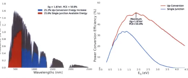
- 1.4 35 1.2 30 E 1.0LU 25 C 0 W 0.8 L 20 C> 0.6 ,- 15 r0 U 0.4 4610 0.2 0.5 0.0 NOa. 500 1000 1500 2000 2500 8.o 0.5 1.0 1.5 2.0 2.5 3.0 3.5 4.0 4.5 Wavelengths (nm) Eg (eV)
(a) Down Conversion Efficiency Increase (b) PCE Limit with Down Conversion Figure 3-3: Down Conversion Efficiency Spectrum and Maximum PCE Curve. (a) With down conversion, the solar cell could utilize about twice more photocurrent where the spectrum Eh, > 2Eg. Due to higher photocurrent in the device, the ex-traction efficiency is also slightly higher, as the blue area is marginally larger in range, which can be seen in 2Eg > Eh, > Eg. (b) The improved PCE for different band gap
energy. As expected, the maximum PCE 41.9% is higher than single junction solar cell maximum PCE 33.7%. Also, optimum band gap Eg = 0.95eV is lower than Eg
= 1.34eV to recycle more energy in the blue region.
In figure 3-3b, PCE limits for different band gap energy are plotted. The maximum
PCE for a down conversion solar cell is 41.9%, which as expected is larger then the
maximum PCE of a single junction solar cell. Note that the optimum band gap for a down conversion solar cell is shifted lower to capitalize more in the high energy part of the solar spectrum with the down converter. In recent years, over 100% energy down conversion yield has been shown [24, 6, 251, making the mechanism a candidate for improving solar cell PCE.
Up Conversion
Energy up conversion is the opposite of down conversion. The up converter could merge two low energy excitation into a high energy 1Eg + !Eg -+ Eg. With an energy up converter, the solar cell could use the non-absorption part of the solar energy spectrum. In figure 3-4a, the collected energy of the optimum up conversion solar cell is plotted. The blue area in the solar spectrum represents the additional gain if
1.8 60
Eg = 1.87eV, PCE = 50.8% -- Up-Conversion
1.6 M 25.2% Up-Conversion Energy increase -- Single junction
25.6% Single junction Available Energy 50
1.4 Maum E 01Eg=1.87eV 1.2 40 PCE=50.8% E 1.0 030 0 0.8 C> 0.6 V 020 0.4 10 0 0.2 500 1000 1500 2000 2500 8.0 0.5 1.0 1.5 2.0 2.5 3.0 3.5 4.0 4.5 Wavelengths (nm) Eg (eV)
(a) Up Conversion Efficiency Increase (b) PCE Limit with Up Conversion
Figure 3-4: Up Conversion Efficiency Spectrum and Maximum PCE Curve. (a) With up conversion, the solar cell could utilize the spectrum in Eg > Eh, > E-. Due to
higher photocurrent in the device, the extraction efficiency is also slightly higher. (b) The improved PCE for different band gap energies with up conversion. As expected, the maximum PCE 50.8% is higher than single junction solar cell maximum PCE
33.7%. The optimum band gap Eg = 1.87eV is higher than Eg = 1.34eV to collect
more energy in the red region.
up converter is added to the solar cell. Similar to the down converter, the additional photocurrent also increases photocurrent extraction. In figure 3-4b, the up conversion solar cell PCE limit is plotted. The maximum PCE for an up conversion solar cell is
50.8%.
Enhancing Efficiency with Down Conversion + Up Conversion
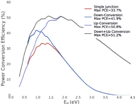
In figure 3-5, the PCE limit of different energy conversion solar cell is compared. The up conversion solar cell has higher maximum PCE than a down conversion so-lar cell. The reason is that the high energy band gap soso-lar cell has relatively less extraction loss. The performance of combined down+up conversion solar cells are also calculated, and as expected, they have an even higher maximum PCE of 51.2% [211. Theoretically, such energy conversions may improve solar cell PCE. Finding and demonstrating efficient energy conversion would be important to realize PCE improvement. In the next section, I will discuss singlet fission and triplet-triplet annihilation, which are pathways to energy down and up conversion.
60 Single Junction Max PCE=33.7% 0-R Down-Conversion Z 50 Max PCE=41.9% Up-Conversion -- Max PCE=50.8% .0 4- Down+Up Conversion 40 Max PCE=51.2% LU o30 20 0 U 0 0 8.0 0.5 1.0 1.5 2.0 2.5 3.0 3.5 4.0 4.5 Eg (eV)
Figure 3-5: PCE Limit of Using Different Energy Conversion Schemes. The PCE limit with down+up conversion is plotted with down conversion, up conversion and a single junction solar cell. As expected, utilizing both down and up conversion increases the maximum PCE (51.2%).
3.2
Physics of Singlet Fission and Triplet-Triplet
An-nihilation
3.2.1
Singlet Fission
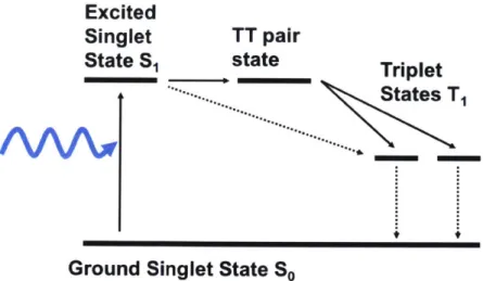
In this thesis, singlet fission [13? , 14? ? ? I is the down conversion mechanism
studied. The basics of the singlet fission process is shown in diagram 3-6. When the triplet state energy ET is about half of the singlet state energy Es, singlet excitons in organic materials may undergo fission which splits them into two triplet excitons. The singlet exciton first transition into a triplet-triplet (TT) pair state [13]. The TT pair state can then dissociate into two triplet excitons, effectively doing energy down conversion. This process can be efficient because direct transition from singlet to triplets are not allowed or very inefficient based on selection rule 2.16. However, the TT pair state is a two particle system with a mixture of 9 possible states. Among the TT pair states, there are some that have singlet characteristics. This allows

![Figure 2-6: Exciton Transport. On the left is Dexter transfer 11], where the electrons in donor LUMO jumps to the acceptor LUMO and the electrons from the accepter HOMO jumps to the donor, effectively moving the exciton](https://thumb-eu.123doks.com/thumbv2/123doknet/14732189.573236/34.917.246.659.138.403/exciton-transport-transfer-electrons-acceptor-electrons-accepter-effectively.webp)