HAL Id: hal-01736053
https://hal.archives-ouvertes.fr/hal-01736053
Submitted on 23 Mar 2018
HAL is a multi-disciplinary open access
archive for the deposit and dissemination of
sci-entific research documents, whether they are
pub-lished or not. The documents may come from
teaching and research institutions in France or
abroad, or from public or private research centers.
L’archive ouverte pluridisciplinaire HAL, est
destinée au dépôt et à la diffusion de documents
scientifiques de niveau recherche, publiés ou non,
émanant des établissements d’enseignement et de
recherche français ou étrangers, des laboratoires
publics ou privés.
Modeling and experiments on diffusion and activation of
phosphorus in germanium
P. Tsouroutas, D. Tsoukalas, I. Zergioti, Nikolay Cherkashin, Alain Claverie
To cite this version:
P. Tsouroutas, D. Tsoukalas, I. Zergioti, Nikolay Cherkashin, Alain Claverie. Modeling and
experi-ments on diffusion and activation of phosphorus in germanium. Journal of Applied Physics, American
Institute of Physics, 2009, 105 (9), pp.094910. �10.1063/1.3117485�. �hal-01736053�
Modeling and experiments on diffusion and activation of phosphorus in germanium
P. Tsouroutas, D. Tsoukalas, I. Zergioti, N. Cherkashin, and A. ClaverieCitation: Journal of Applied Physics 105, 094910 (2009); doi: 10.1063/1.3117485 View online: https://doi.org/10.1063/1.3117485
View Table of Contents: http://aip.scitation.org/toc/jap/105/9 Published by the American Institute of Physics
Articles you may be interested in
Intrinsic and extrinsic diffusion of phosphorus, arsenic, and antimony in germanium Journal of Applied Physics 103, 033508 (2008); 10.1063/1.2837103
Activation and diffusion studies of ion-implanted and dopants in germanium Applied Physics Letters 83, 3275 (2003); 10.1063/1.1618382
High phosphorous doped germanium: Dopant diffusion and modeling Journal of Applied Physics 112, 034509 (2012); 10.1063/1.4745020 Mechanisms of boron diffusion in silicon and germanium
Journal of Applied Physics 113, 031101 (2013); 10.1063/1.4763353 Diffusion of n-type dopants in germanium
Applied Physics Reviews 1, 011301 (2014); 10.1063/1.4838215
On the diffusion and activation of ion-implanted n-type dopants in germanium Journal of Applied Physics 106, 103516 (2009); 10.1063/1.3261838
Modeling and experiments on diffusion and activation of phosphorus in
germanium
P. Tsouroutas,1D. Tsoukalas,1,a兲I. Zergioti,1N. Cherkashin,2and A. Claverie2
1
Department of Applied Physics, School of Applied Sciences, National Technical University of Athens, 15780 Zographou, Greece
2
CEMES/CNRS, 29 rue J. Marvig, 31055 Toulouse Cedex 4, France
共Received 15 December 2008; accepted 12 March 2009; published online 13 May 2009兲
We report on phosphorus diffusion and activation related phenomena in germanium. We have used both conventional thermal processing and laser annealing by pulsed nanosecond Nd:YAG laser. Chemical profiles were obtained by secondary-ion-mass spectroscopy, sheet resistance was estimated by the van der Pauw method, and structural defects were monitored by transmission electron microscopy. Our study covers the temperature range from 440 to 750 ° C, and we were able to efficiently simulate the dopant profiles within that temperature range, taking into account a quadratic dependence of the P diffusion coefficient on the free electron concentration. To achieve that we have taken into account dopant activation dependence on temperature as well as dopant pile-up near the surface and dopant loss owing to outdiffusion during the annealing. A combined laser thermal treatment above the melting threshold prior to conventional annealing allowed the elimination of the implantation damage, so we could perceive the influence of defects on both transient dopant diffusion and outdiffusion. © 2009 American Institute of Physics.
关DOI:10.1063/1.3117485兴 I. INTRODUCTION
Innovative device design and new materials are currently being investigated because of the approaching limit for downscaling CMOS technology. In this context a renewed interest has been observed in germanium as a possible can-didate to replace silicon in future MOSFET technology be-cause of its appealing properties such as higher carrier mobility.1–4 Critical issues concerning diffusion and activa-tion of dopants that will determine the feasibility of germa-nium as the next generation semiconductor material need, however, to be addressed. Until recently data on diffusion studies in the literature were almost half a century old and focused mainly on the p-n junction and sheet resistance measurements.5 The latest reports contribute to a better knowledge of germanium properties. They have shown that while for the p-type dopant 共mostly boron兲 both a well-behaved p+n shallow junction and high activation have been realized6–9 due to low diffusivity共even without annealing兲10 for the n-type dopants 共P, As, and Sb兲, these requirements have not yet been met satisfactorily. Especially in the case of phosphorus, possible reasons for these poor-quality n+p junc-tions are the high P diffusivity7,11,12 and the difference be-tween chemical solubility limit共estimated approximately at 2⫻1020 cm−3 at 600 ° C兲 and the electrical activation 关re-ported at 6⫻1019 cm−3 at 600 ° C 共Ref. 13兲 or 7
⫻1019 cm−3at 800 ° C共Ref.14兲兴 as well as the severe dop-ant loss observed during annealing.7,11,15–20Although recent reports are in general agreement that phosphorus diffusion depends on the square of the electron concentration, the quantitative values deduced for the intrinsic P diffusion co-efficient are different. For example, Chui et al.7reported
sig-nificant higher diffusivities for P diffusion into Ge than did Brotzmann and Bracht12 and Carroll and Koudelka.11
As regards dopant and self-diffusion a rather broad con-sensus on a vacancy assisted mechanism exists, but different views are obtained about the charge state of the defect that mostly influences the dopant movement. Werner et al.21 sug-gested that Ge self-diffusion occurs through single nega-tively charged and neutral vacancies. For the case of dopant diffusion into Ge substrates Vainonen-Ahlgren et al.22 re-ported from their experimental results that As diffusion takes place through doubly negatively charged and neutral vacan-cies. According to Bracht and Brotzmann23 the previous group misinterpreted the diffusion’s quadratic dependence on the free electron concentration in the charge states of vacan-cies, stating that As diffusion in Ge is not sensitive to the properties of vacancies and reporting that arsenic’s diffusion mechanism is through single negatively charged dopant-vacancy pairs. In a recent publication Brotzmann et al.24 re-ported on the existence of doubly negatively charged vacan-cies from their analysis of the simultaneous diffusion of self-and n-type dopant atoms in isotopically controlled Ge multilayer structures, stating that the diffusion of all the com-mon donor dopants共P, As, and Sb兲 is controlled from single negatively charged donor-vacancy pairs that are also respon-sible for the observed enhanced diffusion under extrinsic doping conditions.12On the other hand, Mitha et al.25 ques-tioned even the predominance of vacancy-mediated As dif-fusion.
The present work investigates the diffusion of phos-phorus in Ge that appears in previous studies as the most attractive solution for all n-type dopants. This is because both As and Sb dopants have higher diffusivities7,12and also create more severe damage when introduced in Ge crystal by a兲Electronic mail: [email protected].
JOURNAL OF APPLIED PHYSICS 105, 094910共2009兲
implantation that is more difficult to anneal. These dopants also exhibit lower maximum solid solubility, resulting in higher sheet resistance as compared with phosphorus.15 In order to understand better the influence of implantation dam-age on the dopant loss phenomenon during high temperature treatment, we use a comparative study between implanted only and implanted plus laser-annealed 共LA兲 samples under process conditions that eliminate implantation-induced dam-age. The major part of the paper is then devoted to the esti-mation of P diffusivity through simulation of experimental profiles. For that purpose we have made use of commercial simulators, taking into account not only Fermi level depen-dence of the diffusion coefficient but also the pronounced dopant loss and trapping observed during diffusion in the near surface area. The reduced electrical activation observed from sheet resistance measurements at annealing tempera-tures below 525 ° C is also considered to achieve good agreement with experiments in a wide temperature range.
II. EXPERIMENTAL DETAILS
The substrate wafers used in our study were Ga-doped
p-type Ge of 共1 0 0兲 orientation with a resistivity of
10 ⍀ cm. Phosphorus 共P兲 ions of 1⫻1015 at./cm2 dose were implanted into the Ge substrate at 30 keV energy at room temperature tilted by 7° to the substrate surface normal to minimize the channeling effect. After implantation the wa-fer was dipped into 10% HF in order to obtain a clean sur-face and cut into two pieces.
One part was then split into smaller samples that were LA by a Nd:YAG laser共355 nm兲 using an energy fluence at 4.0 mJ/mm2. The samples were irradiated with five pulses each. The duration of the laser pulses was at 4 ns and the repetition frequency of the pulses was at 1 Hz.
The second part of the initial wafer was capped with a 60 nm thick silicon nitride 共Si3N4兲 layer deposited by sput-tering. After nitride deposition, the wafer was cut into smaller samples with 6⫻6 mm2 area that were furnace-annealed 共FA兲 at temperatures ranging from 440 to 750 °C for 30 min in nitrogen ambient. For comparison reasons some of the LA samples were also nitride-sputtered and FA at 525 ° C for 30 min in nitrogen ambient. The dopant pro-files were monitored by secondary-ion-mass spectrometry 共SIMS兲 using a CAMECA instrument with a Cs+ion primary beam and a net energy of 9 keV. Cross-sectional transmission electron microscopy 共TEM兲 was performed to characterize the structure after major process steps.
III. RESULTS AND DISCUSSION A. Dopant loss
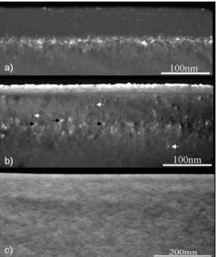
In a previous paper26 we showed that laser annealing above melting of samples implanted with P germanium re-sults in boxlike profiles down to the melting depth owing to high P diffusivity. Unfortunately, we have not been able to completely eliminate extended defects using laser pulses with energy fluence of up to 3.0 mJ/mm2关Fig.1共b兲兴. To that end in the present work we have further increased laser en-ergy, and as we show below, we have achieved a defect-free germanium substrate. In this way when the laser energy
flu-ence is increased to 4.0 mJ/mm2no defects are observed by TEM关Fig.1共c兲兴 and complete recrystallization of the
mate-rial is obtained. Amorphous zone in as-implanted substrates extended down to 65 nm just after P implantation关Fig.1共a兲兴.
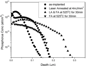
From SIMS measurements shown in Fig. 2 a boxlike profile for the 4.0 mJ/mm2 irradiated sample was observed, indicating melting of the substrate near the surface. The pro-file extended to a depth of 105 nm and the thermal energy delivered to the substrate was sufficient to generate dopant movement even to the tail region of the profile. From dose integration of the SIMS data corresponding to the LA sample, we obtained a dose reduction of 20% as compared with the implanted dose. This reduction is smaller than
re-cently reported results after other thermal
FIG. 1. A series of cross-section TEM images showing共a兲 the as-implanted area,共b兲 the laser spot area irradiated with energy fluence of 3 mJ/mm2,
and共c兲 the laser spot area after irradiated with energy fluence of 4 mJ/mm2.
FIG. 2. SIMS measurements showing phosphorus depth profiles for the as-implanted sample and for the samples irradiated with energy fluences of 3 and 4 mJ/mm2. In order to increase clarity data points shown in the graph
are reduced.
treatments,7,8,15,16,18,20 given that no capping layer was used in our experiment during the laser-annealing process.
Subsequently we deposited by rf sputtering a 60 nm thick silicon nitride layer on top of the LA sample. After sputtering, the LA sample underwent a conventional furnace anneal at 525 ° C. Dopant profile was measured by SIMS 共Fig.3兲.
After integration of the SIMS profile we observed no dopant loss for the LA and FA samples at 525 ° C for 30 min. For exactly the same sputtering and annealing conditions the 共nonirradiated with laser兲, FA only sample exhibited a severe dose loss of about 55%共Fig.3兲. This important difference in
the dose loss behavior between the two above-mentioned conditions can be attributed to implant damage. The LA samples with almost no implant damage present in the Ge lattice exhibited no dopant loss for the same annealing tem-perature and time in contrast with the FA sample that suf-fered implantation-induced damage. Our observation con-cerning the specific experimental conditions is in agreement with the suggestion of Poon et al.18that dose loss could be an effect of implant damage.
The depth profile of the LA and FA samples exhibits two characteristics; the first one is a plateau at the region of the peak concentration, and the second is the fast dopant move-ment toward the substrate occurring at the region between 100 and 240 nm and the existence of a knee at a concentra-tion of about 4.5⫻1018 cm−3below which the abrupt profile indicates a very limited dopant movement. This enhanced dopant diffusion can be attributed to a high diffusivity owing to the increased dopant concentration since the outdiffusion is negligible. This profile is accurately simulated in the next section of this paper using proposed models.
B. Diffusion, activation, and simulation
In a series of experiments we have FA P implanted
samples—using the above reported implantation
conditions—at a wide range of temperatures from 440 to
750 ° C for 30 min in N2 in order to study the diffusion and activation of P in Ge and estimate the respective diffusion coefficient and activation energy. To simulate the experimen-tal profiles the TCAD simulatorTSUPREM IVfrom Synopsys has been used. Our aim during simulation was to capture not only the dopant loss phenomenon but also the dopant pile-up occurring very close to the surface. For this reason the pile-up model proposed by Normand et al.,27which assumes an existence of dopant traps near the surface, was incorpo-rated. It is based on the McNabb and Foster model that con-siders that the traps are capable of capturing and releasing dopant atoms according to the law of thermal equilibrium. Assuming that P共x兲 is the concentration of the traps, which are located at the depth x from germanium surface and ⌽ 共x,t兲 the fraction occupied at time t, the total concentration of the dopants can be expressed as the sum
Ctot共x,t兲 = C共x,t兲 + P共x兲⌽共x,t兲, 共1兲
where C共x,t兲 is the concentration of the impurities. Assum-ing P共x兲=0 outside the pile-up region 共approximately more than 12 nm from the surface兲 and P共x兲= P inside this region, the one-dimensional diffusion equation controlling the dop-ant redistribution is defined as
C共x,t兲 t + P共x兲 ⌽共x,t兲 t = x
冋
D共C兲 C共x,t兲 x册
共2兲 with ⌽共x,t兲 t = kC共x,t兲关1 − ⌽共x,t兲兴 − k⬘
⌽共x,t兲 共3兲The first term kC共x,t兲关1−⌽共x,t兲兴 indicates the rate of cap-ture and the second term k
⬘
⌽共x,t兲 the rate of release inde-pendent of the local concentration of the dopants. k and k⬘
are the respective reaction constants that are assumed to de-pend on the nature of the traps. When k⬘
= 0 the above equa-tion describes a permanent dopant capture. Using as param-eters the concentration of the traps and the depth of the region where they are present as well as the rates of the trapping and detrapping of the diffused dopant atoms, we have managed to simulate this phenomenon to a great extent. The dose loss phenomenon was simulated by depositing a virtual oxide onto the germanium substrate and by control-ling the segregation coefficient between them. In this way we succeeded in confining the surplus dose in the oxide. Then by stripping the oxide we ensured that the correct dopant dose remained in the substrate.The chemical solid solubility limit was set at 2 ⫻1020 cm−3 and the electrical activation at 6.0 ⫻1019 cm−3 for the entire temperature range simulated, which is in accordance with the published reports.13,14 The limited data on the electrical activation for the temperature range considered are, however, a source of error for the cal-culated diffusivity. We have verified with simulation that this error remains small provided the activation level remains close to the one reported in the literature.13,14
The general expression of the diffusion coefficient in extrinsic conditions can be described by the following equa-tion:
FIG. 3. Phosphorus depth profiles obtained by SIMS measurements show-ing the effect of conventional furnace annealshow-ing at temperature of 525 ° C for 30 min both at LA共4 mJ/mm2兲 and as-implanted areas. Depicted data
points are reduced.
D = Do+ D−
冉
n ni冊
+ D−−冉
n ni冊
2 , 共4兲where n represents free electrons and niis the intrinsic
elec-tron concentration.
To obtain an estimation of free electron concentration distribution we performed sheet resistance measurements us-ing the four-point van der Pauw method. The sheet resistance 共Rs兲 is related to free electron distribution 共n兲 profile through
the following equation:
Rs= 1
冕
0 xj q共n兲n共x兲dx . 共5兲The mobility in Eq.共5兲is a function of the electron concen-tration and is calculated using the Hilsum model.28The free electron distribution is first approximated by SIMS measured dopant profile. For each measured value of the sheet resis-tance we can easily calculate by iterations the P concentra-tion above which the dopant atoms are considered inactive and the free electron distribution becomes consequently flat. In TableIwe present for each experimental condition the value of the measured sheet resistance, the calculated sheet resistance value assuming all dopants are active, and the junction depth. It can be observed that for temperatures higher than 600 ° C most of the impurities are active. For that temperature range any concentration above 1019 cm−3 could result in full activation since a very small part of the dopant profile concentration is above this value and conse-quently influences the sheet resistance value slightly. The value chosen to be used in the simulations for the active P concentration threshold for temperatures higher than 600 ° C is set at 6⫻1019 cm−3 to be in agreement with previous studies.13 For 525 ° C the situation is clearer because the corresponding P chemical profile expands to much higher concentrations. It is thus possible to estimate in that case that 1⫻1019 cm−3is the maximum concentration, we can get to have good agreement with measured sheet resistance values since any higher value could lead to inaccurate results.
We note that Hall measurements have been performed in parallel with sheet resistance measurements that reveal each time the conductivity type of the semiconductor. These mea-surements show as expected a n-type material down to 525 ° C, but for 440 ° C the semiconductor type is reversed. This has also been observed by other researchers for
tem-peratures lower than 475 ° C, and it has been attributed to acceptorlike remaining defects after implantation.29
As regards Eq. 共4兲 and in agreement with previous research7,11,12,30the D−−term was sufficient to reproduce ac-curately the experimental profiles for the complete tempera-ture range where a sheet resistance measurement was pos-sible. Our effort to fit the above profiles with the use of neutral共DO兲 and singly charged terms 共D−兲 both separately
and in conjunction produced inaccurate simulation profiles as compared with the experimental ones. For that reason these two diffusivities were set to zero in agreement with the re-sults of Brotzmann and Bracht关see Eq. 共2兲 in Ref.12兴. The
quadratic dependence of the diffusivity on the free electron concentration is because of the charge difference between the mobile P-vacancy pair and the substitutional P donor.23,24In Figs.4共a兲and4共b兲we show the SIMS depth profiles against the diffusion profiles resulting from the simulation for the temperatures of 600, 675, 700, and 750 ° C, respectively. In Fig.5we show the SIMS depth profiles against the simulated profiles for the lower temperatures of 440 and 525 ° C, re-spectively. We remark that the dopant profile distribution at 440 ° C was also accurately simulated using the activation level calculated from the data of 525 ° C.
Using the same activation level as above we have also been able accurately to simulate the furnace-annealing step at
TABLE I. Expected sheet resistance as extracted by SIMS depth profiles against measured sheet resistance with the van der Pauw method and the corresponding junction depth Xj at concentration 1.0⫻1018 cm−3 for all
annealing temperatures ranging from 525 to 750 ° C. Temperature 共°C兲 Expected Rs 共⍀/sq兲 Measured Rs 共⍀/sq兲 Xj 共nm兲 525 70 168 174 600 58 88 228 675 51 60 318 700 56 55 366 750 43 54 467
FIG. 4. SIMS depth profiles after furnace annealing at共a兲 600 and 675 °C and共b兲 700 and 750 °C for 30 min against the best fit simulated profiles 共solid lines兲 obtained by diffusivities reported in this work. Data points are reduced to increase clarity.
525 ° C of the LA sample. This material, as discussed in part A of this section, does not show the presence of any defect prior to the furnace-annealing step and can be considered as an equilibrium situation throughout the complete furnace-annealing time. This simulation is shown in Fig.6.
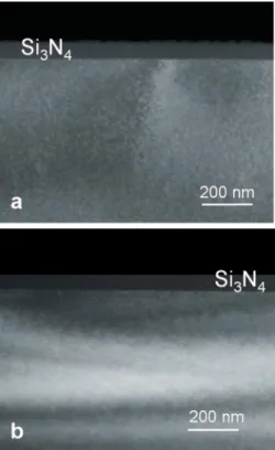
It is interesting to note that for the entire range of the annealing temperatures共440–750 °C兲 the germanium lattice was recovered after the initial damage caused by ion implan-tation with no visible damage 共e.g., extended or EOR de-fects兲 as confirmed by the TEM images 共Fig. 7兲. These are
images from only FA samples at temperatures of 440 and 600 ° C, which show full recrystallization of the germanium crystal. The same applies also to the rest of the temperatures we have used.
C. Discussion
In Fig. 8 we show the intrinsic P diffusion coefficient 共D−兲 deduced from the best fit for each temperature above
600 ° C against the diffusivities extracted for the same tem-perature range from recent investigations of other research groups.7,11,12 The diffusivity coefficient versus temperature shows an Arrhenius behavior with an activation energy of 2.69 eV. We denote here that the linear fit was performed using only three out of the four diffusivity values corre-sponding to the different temperatures used. This approach was followed in order to obtain more accurately the extracted values of pre-exponential coefficient and activation energy since the diffusivity coefficient corresponding to the
tem-FIG. 5. SIMS depth profile after furnace annealing at 440 ° C共opened tri-angle up⌬兲 and 525 °C 共opened triangle down ⵜ兲 for 30 min against the best fit simulated profiles obtained by doubly charged diffusivity model 共solid line兲 considering a maximum electrical activation of 1.0 ⫻1019 cm−2. Data points are reduced.
FIG. 6. Phosphorus depth profile obtained by SIMS measurement after con-ventional furnace annealing at temperature of 525 ° C for 30 min at LA 共4 mJ/mm2兲 area against the best fit simulated profile obtained by doubly
charged diffusivity model共solid line兲 considering a maximum electrical ac-tivation of 1.0⫻1019 cm−2. Depicted data points are reduced for clarity.
FIG. 7. 共Color online兲 Cross-section TEM images showing the structure after furnace annealing at temperature共a兲 440 and 共b兲 600 °C for 30 min. The germanium substrate is fully recrystallized with no visible residual damage.
FIG. 8. Extracted doubly charged diffusivities from simulations’ best fits compared to extrapolated diffusivities from other groups共Refs.7,11, and 12兲 for temperatures ranging from 600 to 750 °C.
perature of 600 ° C is more prone to error, owing to the lower activation level of the dopant at that temperature, as concluded from the results shown in Table I. The extracted activation energy 共2.69⫾0.21 eV兲 and pre-exponential dif-fusion coefficient 共1.44−1.31+15 cm2/sec兲 are higher compared than those reported by Chui et al.7 共2.07 eV, 4.38 ⫻10−2 cm2/sec兲 and Carroll and Koudelka11 共2.3 eV, 1.85
⫻10−2 cm2/sec兲 but lower than those of Brotzmann and Bracht12 共2.85 eV, 9.1 cm2/sec兲. The intrinsic P diffusion coefficients deduced from our experimental profiles are in excellent agreement with the results of Brotzmann and Bracht.12What is more striking from the above comparison is that the result of Chui et al.7 for the diffusivity is about two orders of magnitude higher than the other three reported values. Possible explanations given by Carroll and Koudelka11 for this difference are that these researchers simulated the SRP and not the SIMS profiles, which results in an underestimation of peak concentration, and that they have also scaled the initial dose for each temperature to fit the measured dose after implantation rather than capturing the effect of the dopant loss mechanism on the resulting dop-ant profile. Another plausible explanation for this difference is the use of the different thermal processing approaches, which the above research groups have followed and, mostly, the different implantation conditions used. The diffusivity measured after RTA, an approach used by Chui et al.,7 is probably enhanced owing to implant damage similar to the well-known transient enhanced diffusion 共TED兲 effects ob-served in silicon. By increasing the annealing time the dam-age is annealed, and the diffusivity enhancement has a much smaller contribution to the measured average diffusivity. The source of point defect injection remains to be identified. One can assume either injection from clustering/declustering of P at high concentrations or that point defect source is the dis-solution of extended defects during the annealing steps. It is worth pointing out that the dose used by Chui et al.,7which resulted in extremely high surface concentration for P, was quite high共6⫻1015 cm−2兲 and the energy 20 keV. Damage created after such implantation conditions should behave dif-ferently from damage created by lower implanted doses. Fur-ther studies related to initial implantation damage as a func-tion of dose are necessary. In the study by Carroll and Koudelka11 any influence of TED has been minimized be-cause of the long annealing times used. On the other hand Brotzmann and Bracht12 used diffusion from a solid state P source into Ge substrate where no TED is normally ob-served. At this point we remark that if we make use of a low intrinsic diffusion coefficient value similar to the one re-ported by Brotzmann and Bracht,12 this will result in non-movement of P atoms at intrinsic conditions, something that is experimentally observed from existing data taken from different literature sources.13,20
To investigate the existence of TED under implantation conditions we have performed diffusion anneals for small time intervals 共1 min兲 at 525 °C. The analysis of the SIMS profiles showed no enhanced dopant diffusion to the bulk, demonstrating that for these conditions dopant diffusion is not driven by TED. In addition, simulation of the thermal process of the previously LA sample共Fig.6兲—with no initial
damage present as observed by TEM—gives satisfactory re-sults with the same parameters as FA samples just after im-plantation. This is another evidence of negligible TED at the conditions used in our work.
IV. CONCLUSIONS
Designed experiments using LA samples show an insig-nificant dose loss after additional furnace annealing, which is not the case for only FA samples. It appears that dose loss is associated with implantation damage annealing that drives P atoms out of Ge. The implantation damage in our experimen-tal conditions can be annihilated for temperatures as low as 440 ° C, as confirmed by TEM. Simulation of experimental P profiles obtained after annealing in a wide temperature range gives satisfactory results, taking into account a quadratic de-pendence of the P diffusion coefficient on the free electron concentration that is in accord with the vacancy mechanism of P diffusion in Ge proposed by Brotzmann et al.12,24 In addition, a segregation coefficient between the cap nitride and Ge substrate modulating the dose loss and a pile-up model to capture the increased dopant concentration very close to the Ge surface was considered. For temperatures below 525 ° C a limited electrical activation needs to be con-sidered due to reduced solid solubility in order to obtain accurate fit to experimental profiles. The estimated intrinsic P diffusion coefficient is close to the value reported by other researchers11,12 with an activation energy of 2.69 eV.
ACKNOWLEDGMENTS
Two of the authors 共P.T. and D.T.兲 would like to ac-knowledge financial support from Greek GSRT and ST Mi-croelectronics through the PENED program and also Dr. Claude Armand from INSA-Toulouse and Dr. G. Bennas-sayag CEMES-Toulouse for SIMS measurements.
1C. O. Chui, H. Kim, D. Chi, B. B. Triplett, P. C. McIntyre, and K. C.
Saraswat, Tech. Dig. – Int. Electron Devices Meet. 2002, 437.
2H. Kim, C. O. Chui, K. Saraswat, and P. C. McIntyre,Appl. Phys. Lett.83,
2647共2003兲.
3H. Shang, H. Okorn-Schmidt, J. Ott, P. Kozlowski, S. Steen, E. C. Jones,
H. S. Wong, and W. Hanesch,IEEE Electron Device Lett.24, 242共2003兲.
4A. Ritenour, S. Yu, M. L. Lee, N. Lu, W. Bai, A. Pitera, E. A. Fitzgerald,
D. L. Kwong, and D. Antoniadis, Tech. Dig. – Int. Electron Devices Meet. 2003, 433.
5N. A. Stolwijk and H. Bracht, Diffusion in Silicon, Germanium and Their
Alloys, Landolt-Börnstein New Series Vol. III/33 共Springer, New York, 1998兲.
6Germanium-Based Technologies–From Materials to Devices, edited by C.
Claeys and E. Simoen共Elsevier, Amsterdam, 2007兲.
7C. O. Chui, K. Gopalakrishnan, P. B. Griffin, J. D. Plummer, and K. C.
Saraswat,Appl. Phys. Lett.83, 3275共2003兲.
8A. Satta, E. Simoen, T. Clarysse, T. Janssens, A. Benedetti, B. De Jaeger,
M. Meuris, and W. Vandervorst,Appl. Phys. Lett.87, 172109共2005兲.
9Y. S. Suh, M. S. Carroll, R. A. Levy, G. Bisognin, D. De Salvador, and M.
A. Sahiner, IEEE Trans. Electron Devices 52, 2416共2005兲.
10S. Uppal, A. F. W. Willoughby, J. M. Bonar, A. G. R. Evans, N. E. B.
Cowern, R. Morris, and M. G. Dowsett,J. Appl. Phys.90, 4293共2001兲.
11M. S. Carroll and R. Koudelka,Semicond. Sci. Technol.22, S164共2007兲. 12S. Brotzmann and H. Bracht,J. Appl. Phys.103, 033508共2008兲. 13A. Satta, T. Janssens, T. Clarysse, E. Simoen, M. Meuris, A. Benedetti, I.
Hoflijk, B. De Jaeger, C. Demeurisse, and W. Vandervorst, J. Vac. Sci. Technol. B24, 494共2006兲.
14V. I. Fistul, A. G. Yakovenko, A. A. Gvelesiani, V. N. Tsygankov, and R.
L. Korchazhkina, Inorg. Mater. 11, 457共1975兲.
15E. Simoen, A. Satta, A. D’Amore, T. Janssens, T. Clarysse, K. Martens, B.
De Jaeger, A. Benedetti, I. Hoflijk, B. Brijs, M. Meuris, and W. Vander-vorst,Mater. Sci. Semicond. Process.9, 634共2006兲.
16A. Satta, E. Simoen, T. Janssens, T. Clarysse, B. De Jaeger, A. Benedetti,
I. Hoflijk, B. Brijs, M. Meuris, and W. Vandervorst,J. Electrochem. Soc. 153, G229共2006兲.
17C. Jasper, L. Rubin, C. Lindfors, K. S. Jones, and J. Oh, Proceedings of
Ion Implantation Techniques共IEEE, New York, 2002兲, p. 548.
18C. H. Poon, L. S. Tan, B. J. Cho, and A. Y. Du.J. Electrochem. Soc.152,
G895共2005兲.
19T. Janssens, C. Huyghebaert, D. Vanhaeren, G. Winderickx, A. Satta, M.
Meuris, and W. Vandervost,J. Vac. Sci. Technol. B24, 510共2006兲.
20A. Chroneos, D. Skarlatos, C. Tsamis, A. Christofi, D. S. McPhail, and R.
Hung,Mater. Sci. Semicond. Process.9, 640共2006兲.
21M. Werner, H. Mehrer, and H. D. Hochheimer,Phys. Rev. B32, 3930
共1985兲.
22E. Vainonen-Ahlgren, T. Ahlgren, J. Likonen, S. Lehto, J. Keinonen, W.
Li, and J. Haapamaa,Appl. Phys. Lett.77, 690共2000兲.
23H. Bracht and S. Brotzmann, Mater. Sci. Semicond. Process. 9, 471
共2006兲.
24S. Brotzmann, H. Bracht, J. Lundsgaard Hansen, A. Nylandsted Larsen, E.
Simoen, E. E. Haller, J. S. Christensen, and P. Werner,Phys. Rev. B77, 235207共2008兲.
25S. Mitha, M. J. Azizb, D. Schiferl, and D. B. Poker,Appl. Phys. Lett.69,
922共1996兲.
26P. Tsouroutas, D. Tsoukalas, A. Florakis, I. Zergioti, A. A. Serafetinides,
N. Cherkashin, B. Marty, and A. Claverie,Mater. Sci. Semicond. Process. 9, 644共2006兲.
27P. Normand, D. Tsoukalas, N. Guillemot, and P. Chenevier,J. Appl. Phys.
66, 3585共1989兲.
28C. Hilsum,Electron. Lett.10, 259共1974兲.
29K. Benourhazi and J. P. Ponpon,Nucl. Instrum. Methods Phys. Res. B71,
406共1992兲.
30M. Naganawa, Y. Shimizu, M. Uematsu, K. M. Itoh, K. Sawano, Y.
Shiraki, and E. E. Haller,Appl. Phys. Lett.93, 191905共2008兲.