HAL Id: tel-02378303
https://tel.archives-ouvertes.fr/tel-02378303
Submitted on 25 Nov 2019HAL is a multi-disciplinary open access archive for the deposit and dissemination of sci-entific research documents, whether they are pub-lished or not. The documents may come from teaching and research institutions in France or abroad, or from public or private research centers.
L’archive ouverte pluridisciplinaire HAL, est destinée au dépôt et à la diffusion de documents scientifiques de niveau recherche, publiés ou non, émanant des établissements d’enseignement et de recherche français ou étrangers, des laboratoires publics ou privés.
nanotube composite for next generation on-chip energy
efficient interconnect applications
Jie Liang
To cite this version:
Jie Liang. Exploration of carbon nanotube and copper-carbon nanotube composite for next genera-tion on-chip energy efficient interconnect applicagenera-tions. Micro and nanotechnologies/Microelectronics. Université Montpellier, 2019. English. �NNT : 2019MONTS022�. �tel-02378303�
TH`
ESE POUR OBTENIR LE GRADE DE DOCTEUR
DE L’UNIVERSIT´
E DE MONTPELLIER
En Micro´electronique
´
Ecole doctorale : Information, Structures, Syst`emes
Unit´e de recherche LIRMM
Exploration of Carbon Nanotube and
Copper-Carbon Nanotube Composite for Next
Generation On-chip Energy Efficient Interconnect
Applications
Pr´
esent´
ee par Jie LIANG
le 17 Juin 2019
Sous la direction de Aida TODRI-SANIAL
Devant le jury compos´e de
Pascal Nouet Professeur LIRMM, UMR CNRS / Universit´e de Montpellier Pr´esident du Jury Aida Todri-Sanial Directrice de Recherche LIRMM, CNRS / Universit´e de Montpellier Directrice de th`ese
Ian O’Connor Professeur Ecole Centrale de Lyon´ Rapporteur
Jacques-Olivier Klein Professeur Universit´e Paris-Sud Rapporteur
Cristell Maneux Professeur Universit´e de Bordeaux Examinatrice
I dedicate my dissertation work to my family and many friends. A special feeling of gratitude to my loving parents, whose words of encouragement and push for
R´
esum´
e
Dans les soci´et´es modernes, le style de vie rapide et efficace n´ecessite un ´echange
d’informations rapide, pr´ecis et sˆur. Cette masse d’information est acquise par le
biais de divers dispositifs reposant en grande majorit´e sur des r´eseaux ´electroniques complexes ainsi que sur Internet. La ville intelligente, l’Internet des objets (IoT) et l’intelligence artificielle des objets (AIoT) sont actuellement des tendances essen-tielles du d´eveloppement technologique futur. L’informatique quantique et neuro-morphique `a tr`es grande vitesse laisse entrevoir la possibilit´e de reprendre les archi-tectures de Von Neumann. Cependant, tous ces ´evolutions consomment une ´enorme quantit´e d’´energie. Satisfaire `a la fois les hautes performances et les ultra-basses con-sommation est au centre des d´efis pos´es aux technologies de la prochaine g´en´eration. Afin de r´epondre `a la demande en termes de quantit´e de donn´ees et d’efficacit´e ´energ´etique, la miniaturisation des produits micro´electroniques, plus pr´ecis´ement
des transistors, coupl´ee `a une am´elioration des fonctionnalit´es et un coˆut r´eduit,
ouvre la possibilit´e de r´epondre aux demandes susmentionn´ees.
Cependant, l’am´elioration seule des performances des transistors des prochaines g´en´erations de puce n’est pas suffisante. Malgr´e leurs importances, les puces en elles-mˆemes ne repr´esentent qu’une petite partie du tr`es vaste et complexe puz-zle de la technologie de l’information. Ainsi, pour fa¸conner l’avenir du monde num´erique, nous devons ´egalement examiner la situation dans son ensemble. Les performances des transistors ne valent que dans le syst`eme dans lequels ils sont int´egr´es. Les microprocesseurs les plus rapides sont inutiles si la capacit´e des lignes de donn´ees n’est pas augment´ee en cons´equence. C’est l`a que les interconnexions ´electriques en cuivre (Cu) actuelles approcheront leurs limites physiques et pour-raient ne plus ˆetre en mesure de suivre le d´ebit de donn´ees d’un processeur. En fait, la fr´equence de fonctionnement des processeurs d’aujourd’hui est d´ej`a r´egie par les retards d’interconnexion et, en cours de fonctionnement, la plus grande partie de leur puissance est dissip´ee dans les interconnexions. Par cons´equent, le manque d’interconnexions am´elior´ees est `a l’origine de la tendance actuelle `a une simple r´eduction de la taille des circuits sans mise `a l’´echelle simultan´ee des performances de la technologie CMOS, contrairement aux d´ecennies pr´ec´edentes.
Parall`element `a la forte augmentation de la r´esistance des cˆables d’interconnexion induite par la diminution des dimensions, les performances globales d’une puce se trouve domin´ees par les interconnexions pour la r´egion submicronique. Par-all`element `a la miniaturisation de la taille caract´eristiques des dispositifs, le d´elai intrins`eque de porte diminue et le d´elai d’interconnexion augmente consid´erablement
et devient dominant pour les performances globales. Ob´eissez `a la loi de Moore [110]
optimis´es mais que ceux-ci ne disposent pas des interconnexions appropri´ees. Par cons´equent, l’exploration et la recherche de mat´eriaux alternatifs pour conducteurs d’interconnexion sur puce sont essentielles et n´ecessaire pour les futures puces hautes performances et faible consommation.
Pendant plusieurs d´ecennies, l’aluminium (Al) a ´et´e utilis´e pour les
intercon-nexions sur puce. En raison des contraintes de mise `a l’´echelle des fils et de
faible r´esistances des fils, le cuivre, avec sa faible r´esistivit´e, son faible coˆut et
moins d’oxydation que l’aluminium, a ´et´e jusqu’`a pr´esent la silution privil´egi´ee pour les fils d’interconnexion. Cependant, avec la r´eduction continue de la largeur de ligne des interconnexions en Cu, les performances et la fiabilit´e des conduc-teurs d’interconnexion requi`erent une attention particuli`ere pour suivre la mise `a l’´echelle des transistors. L’avancement de la photolithographie par fil m´etallique est ´egalement une composante importante du d´efi pos´e, la rugosit´e de la surface augmentant avec la largeur de raie du m´etal. Une densit´e de courant ´elev´ee en-traˆınera la rupture du mat´eriau d’interconnexion le long du chemin conducteur, ce qui provoquera ´egalement un dysfonctionnement du circuit et acc´el´erera le d´elai de la puce. Les deux probl`emes principaux des interconnexions actuelles en Cu sont la r´esistivit´e consid´erablement accrue et l’effet d’´electromigration important, qui posent les limites physique des interconnexions en Cu.
Le cuivre en tant qu’interconnexion sur puce suivant un proc´ed´e damasc`ene afin de r´eduire davantage la r´eduction d’´echelle. Cependant, l’existence d’une couche barri`ere de tranch´ees d’interconnexion en Cu est n´ecessaire et ne peut ˆetre r´ealis´ee en dessous d’une certaine ´epaisseurs(∼2 nm); par cons´equent, la fraction effective des lignes de Cu diminue consid´erablement si des lignes tr`es minces avec une barri`ere induisent une augmentation importante de la r´esistance, encore moins de r´esistance `a l’´electromigration (EM) et en cons´equence une d´egradation des performances encore plus s´ev`ere. Par cons´equent, il est propos´e que des m´etaux alternatifs tels que le Ruthenium (Ru) et le Cobalt (Co) remplacent le Cu en conservant le proc´ed´e de Damas. Mˆeme si Ru et Co ont une r´esistivit´e sup´erieure `a celle de Cu, du fait qu’ils ne poss`edent pas de barri`ere, la r´esistance effective `a la tranch´ee est inf´erieure `a celle du Cu.
Le Graphene a ´et´e d´ecouvert en 2004 [116]. Le graph`ene est un arrangement
en r´eseau hexagonal monocouche d’atomes de carbone. En raison de sa nature
semi-m´etalliques et des propri´et´es particuli`eres qui en d´ecoulent, o`u la bande de
conduction et la bande de valence se croisent au point de Dirac, ses ´electrons se comportent comme des fermions de Dirac sans masse qui produisent du graph`ene ayant une vitesse de transport et une densit´e de courant ´elev´ees. Par cons´equent, de nombreuses recherches sur le graph`ene sont conduites pour des applications ciblant les dispositifs micro-´electroniques et les interconnexions. Une bande ´etroite de graph`ene, connue sous le nom de graphene nanoribbon (GNR), a ´et´e ´etudi´ee
comme candidat prometteur pour remplacer les canaux de transistors [11, 117] et
les interconnexions [130] pour les circuits int´egr´es de tr`es grande taille de prochaine
g´en´eration (VLSI) . Le GNR pr´esente de nombreux avantages sur les propri´et´es
mo-bilit´e des porteurs et une conductivit´e thermique [134]. Le libre parcours moyen des
´electrons dans du GNR peut atteindre plusieurs microm`etres [15] et sa conductivit´e
thermique est dans la gamme de 5300 W/mK. Cependant, Le GNR a des propri´et´es m´etalliques ou semi-conductrices en fonction de la disposition des atomes de bord. Un GNR `a bords en zigzag se comporte de mani`ere m´etallique et `a ”bord de
fau-teuils” est semi-conducteur [112]. Il reste encore difficile de fabriquer des GNR
enti`erement m´etalliques de haute qualit´e pour les applications d’interconnexion `a grande ´echelle. Cependant, en raison de la quantification 2D et de la bande inter-dite ´etroite du GNR semi-conducteur, `a la temp´erature ambiante ou au-dessus, la transition des ´electrons induite par les effets thermiques peut rendre la bande inter-dite ´etroite n´egligeable. Les GNR deviennent l’une des alternatives int´eressantes et prometteuses pour les futures applications d’interconnexions sur puce.
Le nanotube de carbone (CNT) a ´et´e d´ecouvert sous la forme de parois
mul-tiples (MWCNT) en 1999 [63] par le chercheur japonais S. Iijima. Les CNT `a
paroi simple (SWCNT) sont d´ecouverts deux ans apr`es en 1993 [64, 17]. Le CNT
peut ˆetre vu comme enveloppant une ou plusieurs feuilles de graph`ene dans un fil cylindrique `a une dimension, la distance entre les coquilles est d´efinie par la
dis-tance de Van der Waals (0,34 nm) [45, 46]. Le diam`etre des SWCNT peut varier
de 0,4 nm `a 4 nm (le diam`etre typique est de 1,4 nm). Le diam`etre de coque le plus `a l’ext´erieur de MWCNT peut aller jusqu’`a 100 nm. Le CNT en tant que fil quantique 1-D, poss`ede une tr`es forte liaison covalente entre atomes de carbone
[166], ce qui lui conf`ere un tr`es bon confinement des ´electrons dans la direction
uni-axiale. Les CNT ont ´egalement des propri´et´es physiques uniques: un tiers d’entre eux sont m´etalliques et les autres sont semi-conducteurs en fonction de leur
chi-ralit´e [165, 131]. Les CNT m´etalliques ont de tr`es bonnes propri´et´es pour les
ap-plications d’interconnexion, telles que le transport balistique, le chemin libre moyen
des ´electrons (jusqu’`a plusieurs), r´esistance m´ecanique ´elev´ee (∼ 1 TPa) [132, 88],
ampoule ´elev´ee (jusqu’`a 109); ) [161, 171] et `a haute conductivit´e thermique (de
2000 W/mK `a 7500 W/mK) [66]. Cependant, les CNT ont toujours des probl`emes
de fiabilit´e en ce qui concerne les processus de fabrication et la conception. Au cours des derni`eres d´ecennies, des chercheurs ont ´etudi´e les ph´enom`enes de basse
temp´erature (densit´e, int´egrit´e), de densit´e ´elev´ee (>1013 cm−2) [151, 44, 118],
pro-cessus de croissance de haute qualit´e. Les contrˆoles de l’orientation des CNT [151,
44, 145] N´eanmoins, la s´electivit´e de la chiralit´e [160, 59, 170] des CNT avec un
processus d´evelopp´e par CVD `a basse temp´erature reste un d´efi important pour les int´egrations en bout de ligne (BEOL) compatibles avec les processus silicium.
L’objectif de cette th`ese est d’explorer le potentiel des nanotubes de carbone et des composites de nanotubes de carbone pour les interconnexions faible consomma-tion de la prochaine g´en´eraconsomma-tion. Sur la base des mod`eles compacts physiques de pointe pour les CNT immobiles en SW et MW, nous avons tout d’abord d´evelopp´e un mod`ele compact am´elior´e bas´e sur la physique ´electrique en tenant compte de l’effet de dopage et de la variabilit´e des CNT autonomes pour une utilisation en tant qu’interconnexions locales. Deuxi`emement, nous avons explor´e le dopage des CNT, qui ´etait l’un des principaux objectifs pour comprendre comment contrˆoler indi-rectement l’incertitude de la chiralit´e des CNT et am´eliorer davantage leurs conduc-tivit´es et att´enuer les d´efauts des contacts critiques. Nos mod`eles ´etablis dans cette
CNT et des CNT-Cu pour les utilisations d’interconnexions interm´ediaires et glob-ales. En raison de la densit´e de courant ´elev´ee fournie, l’effet thermique des in-terconnexions (auto-´echauffement) est l’un des principaux facteurs des probl`emes d’´electromigration et de la d´efaillance des interconnexions. Enfin, nous avons int´egr´e nos mod`eles ´electriques `a des points de r´ef´erence de circuits afin d’´evaluer leurs per-formances et leurs efficacit´es ´energ´etiques, que nous avons ensuite compar´e avec des interconnexions en Cu. Cette th`ese fait partie de et a ´et´e financ´ee par la Commis-sion europ´eenne. Le projet europ´een Horizon 2020 CONNECT est financ´e par la subvention 688612. Le projet CONNECT est une collaboration entre l’Universit´e de Glasgow (UoG), Royaume-Uni; LIRMM-CNRS, France; CEA Leti / Liten, France; Fraunhofer (FhG), Dresde, Allemagne; Synopsys, Royaume-Uni; AIXTRON Ltd., Cambridge, Royaume-Uni; et IBM Suisse.
Cette th`ese porte principalement sur la mod´elisation compacte et les simulations au niveau du circuit en prenant des entr´ees `a partir des r´esultats de la simulation au niveau atomistique fondamental (UoG) et en fournissant des retours aux partenaires exp´erimentaux (CEA et FhG) pour le guidage des exp´eriences et la validation des mod`eles. Un autre aspect majeur consiste `a fournir des directives de conception de niveau de circuit pour l’utilisation des interconnexions `a base de CNT.
Au chapitre 2, nous d´ecrivons les mod`eles compacts primitifs de r´esistance (R) et de capacitance (C) des CNT bas´es sur des travaux de litt´erature. Nous constituons une base solide en ´etudiant des mod`eles de base RC `a CNT `a une seule paroi (SW) et `a plusieurs parois (MW). EN compl´ement, nous proposons une ´etude approfondie des variations de processus et de leur impact sur les performances d’interconnexion du r´eseau MWCNT.
Au chapitre 3, nous ´evaluons la performance et la variabilit´e des interconnexions du r´eseau MWCNT tout en tenant compte de l’impact du dopage. Nous introduisons
le param`etre nombre de canaux conducteurs (NC) et l’int´egrons dans notre mod`ele
compact am´elior´e de MWCNT d´ecrit au chapitre 2. En calculant th´eoriquement NC
en fonction du d´ecalage de niveau de Fermi Ef - nous ´evaluons chaque source de
variation (diam`etre, chiralit´e, d´efauts) et toutes sources en utilisant des simulations de Monte Carlo (MC). Les r´esultats de la simulation sont ensuite compar´es aux r´esultats exp´erimentaux et une bonne coh´erence est trouv´ee entre eux.
Au chapitre 4, nous avons commenc´e par ´etudier s´epar´ement les propri´et´es thermo-´electriques des Cu, SWCNT, MWCNT, SWCNT-Cu composite et MWCNT-Cu composite. Nous construisons des mod`eles thermo´electriques pour chacun des cas en incluant des effets d’auto-´echauffement, de diffusion de la chaleur vers le substrat. Un syst`eme d’´equation diff´erentielle `a conduction thermique `a composi-tion automatique est r´esolu pour extraire le profil de temp´erature pour chaque cas d’interconnexion. De plus, nous avons d´eduit leurs caract´eristiques I-V et leurs vari-ations de r´esistance sous diverses tensions. L’ampacit´e est calcul´ee `a la fin afin de comprendre les propri´et´es thermo´electriques du mat´eriau. Cette ´etude n´ecessite des validations suppl´ementaires avec des donn´ees exp´erimentales.
Dans le chapitre 5, nous cherchons `a mieux comprendre les performances au niveau du circuit des interconnexions MWCNT dop´ees et le potentiel des
technolo-gie carbone, en comparant CNTFET + MWCNT et FinFET + Cu, pr´esent´e en tant qu’´etude de cas pour les technologies avanc´ees. Les mod`eles d’interconnexion MWCNT, CNTFET, 7 nm FinFET et PTM Cu model sont utilis´es pour effectuer des simulations au niveau circuit. Le retard de circuit global, le produit de retard de puissance et d’´energie sont ´etudi´es pour les deux cas d’´etude. De plus, un cir-cuit logique (additioneur/Full-Adder) est pris en exemple pour ´etudier et comparer diff´erents choix d’interconnexions: interconnexions id´eales, interconnexions en Cu et interconnexions MWCNT.
Une ouverture sur les nouvelles perspectives d’investigation des technologie `a base de nano-tubes de carbones terminent le pr´esent manuscrit de th`ese
Acknowledgments
Undertaking this PhD has been a truly life-changing experience for me and it would not have been possible to do without the support and guidance that I received from many people.
I would like to first say a very big thank you to my supervisor Dr. Aida Todri-Sanial for all the support and encouragement she gave me. She helped me become mature both in science and in personal life. Without her guidance and constant feedback this PhD would not have been achievable.
I am grateful to the funding received from EU H2020 to undertake my PhD, which opened my vision of science and how important teamwork is for the research. My thanks also go out to the support I received from the collaborative work I undertook with all my collaborators in the project CONNECT.
I am indebted to all my friends and family in France and China who opened their arms to me during my difficult time and who were always so helpful in numerous ways.
I would also like to say a heartfelt thank you to my Mum and Dad for always believing in me and encouraging me to become a better person in life.
Contents
R´esum´e v
Acknowledgements xi
List of Figures xv
List of Tables xxiii
1 Introduction 1
1.1 Overview of On-Chip Interconnects . . . 1
1.2 Copper Interconnects . . . 3
1.2.1 Copper Interconnects - Resistivity . . . 3
1.2.2 Copper Interconnects - Electromigration . . . 4
1.3 Emerging Interconnects for Advanced Technology Node . . . 5
1.3.1 Metal Interconnects: Cobalt and Ruthenium . . . 5
1.3.2 Graphene Nanoribbon Interconnects . . . 8
1.3.3 Carbon Nanotube Interconnects . . . 8
1.4 Structure of the Thesis . . . 11
2 Pristine Carbon Nanotubes 15 2.1 Introduction . . . 15
2.2 Physical Description of Carbon Nanotube . . . 16
2.3 Pristine CNT Resistance and Capacitance . . . 19
2.3.1 Pristine SW/MW CNT resistance . . . 19
2.3.2 Pristine SW/MW CNT capacitance model . . . 21
2.4 Sources of Variability on MWCNT . . . 22
2.4.1 Diameter Variations . . . 22
2.4.2 Defect Occurrence . . . 24
2.4.3 CNT Chirality . . . 25
2.4.4 Shells Connection to Contacts . . . 25
2.5 Enhanced MWCNT Model . . . 26
2.5.1 Original MWCNT Distributed Compact Model . . . 26
2.5.2 Enhanced MWCNT Distributed Compact Model . . . 27
2.5.3 Enhanced MWCNT Lumped Compact Model . . . 28
2.6 MWCNT Variability Evaluations . . . 29
2.6.1 Simulation setup . . . 29
2.6.5 MWCNT Shell to Contact Variations . . . 34
2.7 Conclusion . . . 35
3 Doping of Carbon Nanotubes 37 3.1 Introduction . . . 37
3.2 Electrical Compact Models . . . 38
3.2.1 Doping of MWCNT . . . 39
3.2.2 Atomistic model - DFT Calculation . . . 39
3.2.3 Electrical RC model . . . 41
3.2.4 Analytical Method for Computing the Impact of Doping . . . 43
3.3 Evaluations of Variability with Doping . . . 46
3.3.1 Simulation Setup . . . 46
3.3.2 Impact of MWCNT Doping . . . 47
3.3.3 Comparisons with Experimental Data . . . 50
3.3.4 Doping Efficiency . . . 53
3.3.5 MWCNT Shell to Contact Variations . . . 54
3.4 Experimental vs. Simulation Results . . . 55
3.5 Discussion . . . 61
3.6 Conclusion . . . 62
4 Copper-Carbon Nanotube Composite 65 4.1 Introduction . . . 65
4.2 Copper, and CNT Electrical-Thermal Properties . . . 67
4.2.1 Copper electrical-thermal transport . . . 67
4.2.2 Thermal transport in CNT . . . 68
4.3 Electrical-thermal Modeling and Simulation results . . . 70
4.3.1 Electrical-thermal model & simulation results in Cu . . . 70
4.3.2 Electrical-thermal model & simulation results in CNTs . . . . 73
4.3.3 Electrical-thermal model in Cu-CNT composite . . . 77
4.3.4 Thermal effect simulation results of Cu-CNT composite . . . . 79
4.4 Discussion . . . 84
4.5 Conclusion . . . 86
5 Circuit Level Analysis of Carbon Nanotube Interconnects 89 5.1 Introduction . . . 89
5.2 Contacts of CNTs Interconnects . . . 90
5.2.1 Different Contacts for MWCNT . . . 90
5.3 CNT Interconnects in Simple Test Benchmark: Inverter to Inverter . 92 5.3.1 Testcase I: CNTFET devices with MWCNT interconnect . . . 94
5.3.2 Testcase II: FinFET devices with Cu interconnect . . . 94
5.3.3 Variability Evaluations of CNTs in test benchmarks . . . 95
5.4 CNT Interconnects in Larger Test Benchmark: Full-adder. . . 100
5.4.1 Full-adder characterization . . . 100
5.5 Discussion . . . 102
6 Conclusion and Perspective 107
6.1 Conclusion . . . 107
6.2 Research Perspectives. . . 109
6.2.1 To complete this thesis . . . 109
6.2.2 Perspectives relating to Carbon Nanotube . . . 109
6.2.3 Perspectives relating to Energy Efficiency. . . 110
Appendix 113
Curriculum Vitae 119
List of Figures
1.1 On-Chip hierarchical cross-sectional interconnect structure [1]. . . 2 1.2 Interconnect delay becomes dominant for submicron region [100]. . . 3 1.3 (a) Copper interconnects suffer from grain boundary and surface
scat-tering effects. (b) Grain boundary and scatscat-tering effects increase Cu interconnects resistivity with shrinking of Cu width [77]. . . 4 1.4 (a) Formation of electromigration for a bulk metal interconnect. (b)
Scaling induced more electromigration effects, voids and breaks are dominant for Cu interconnects performance and lifetime. . . 5 1.5 A brief history of Carbon Nanotube. . . 10 2.1 Carbon nanotube, based on different rolling direction, can have three
types of chirality: chiral, armchair and zigzag. Chirality of carbon nanotube is defined by chiral vector ~C which composed by indices n, m and unit vector ~a1 and ~a2. . . 17 2.2 Carbon nanotubes can be formed as single-walled (SWCNT) or
multi-walled (MWCNT). MWCNT can be seen as coaxial SWCNT shells with different diameters. . . 18 2.3 Typical Energy Band Structure of (a) metallic and (b) semiconductor
carbon nanotube. . . 18 2.4 Resistance of pristine SWCNT varies with its diameter and length
(diameter varying from 1 nm to 20 nm; length varying from 0.5 µm to 5 µm). . . 20 2.5 MWCNT conductivity with and without tunnelling effect. . . 21 2.6 Experimental results of MWCNT DCN T maxvariation. Mean and
stan-dard deviation of DCN T max are 7.8 nm and 1.6 nm, respectively. . . . 23 2.7 Experimental results of numbers of shells for MWCNTs of different
outermost (external) diameters. Also shown are the calculation re-sults of Equation (2.11). . . 24 2.8 Atomistic-level simulation results of defect-induced resistance of a
SWCNT (24, 0) with 6 vacancies. The SWCNT length is set to be about 42 nm corresponding to a vacancy density of 0.143 /nm. Also shown is the corresponding LogN fit result. . . 24
rameters are contact resistance RCON and defect-induced resistance RDef in each shell. Except RCON and lumped quantum resistance RQ, each shell has intra-shell distributed parameters including RDef and scattering resistance Rs, kinetic inductance LK, and quantum ca-pacitance CQ. Inter-shell parameters include tunneling conductance GT and shell-to-shell capacitance CS. Intra-shell parameters have p components while inter-shell parameters have p-1 components. Only the outermost shell has electrostatic capacitance CE with the ground. Rtand Cout are the effective resistance and output capacitance of the driver, respectively, and Cload is the input capacitance of the load [91]. 26 2.10 Dependence of Pd-SWCNT end-contact resistance on cross-sectional
area of SWCNT. . . 28 2.11 Enhanced lumped p-shell MWCNT compact model proposed based
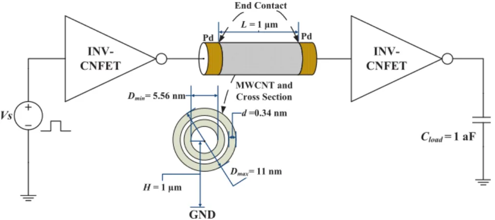
on the enhanced distributed compact model in Fig. 2.9. Driver and load are not shown for clarity. . . 29 2.12 Simulation setup schematic of MWCNT as an interconnect. MWCNT
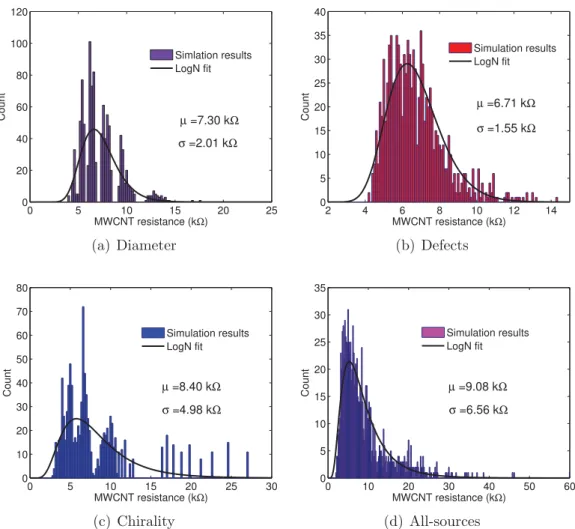
connects two inverters composed of CNTFET devices. . . 29 2.13 (a)-(d) are distributions of resistance variation of the pristine MWCNT
interconnect with input diameter, defects, chirality and all-sources variations respectively. . . 31 2.14 (a)-(d) are PDFs of resistance, delay, power and PDP of the
pris-tine MWCNT interconnect respectively with input diameter, defects, chirality and all-sources variations. . . 32 2.15 Change of resistance while varying defect density on pristine MWCNT
interconnects with diameter, defect, chirality and all-sources variations. 33 2.16 Minimizing resistance variation of the pristine MWCNT interconnect
by reducing the contribution of diameter and defect variations. . . 34 2.17 Change of (a) resistance and delay, (b) power and PDP of MWCNT
with disconnected CNT shells from contact. In this example, there are total nine shells in the MWCNT. . . 35 3.1 Comparison of the formation energy (Ef orm) for the PtCl4 doped
CNT(15,0). Grey, white, and green spheres are carbon, platinum, and chlorine, respectively [93]. . . 40 3.2 Band structure and total DOS of pristine and PtCl4 doped (a) CNT
(15,0) (See Fig 1. b)). Fermi-level (Ef) is set to 0.0 eV. Due to the dopant, Ef is shifted by -0.6 eV, and DOS near Ef has increased. (b) CNT (16,0). Ef shifts by dopants, semiconductor CNT (16,0) has become a metal [93]. . . 40 3.3 7nm diameter MWCNT conductivity with different doping levels where
3.4 a) NC of metallic shells and b) NC of semiconducting shells with the Ef shift for the MWCNT with 11 nm outermost diameter, and c) NC of metallic and semiconducting shells of the outermost (11 nm) and the innermost (5.56 nm) shells before and after the Ef shift (similar for the negative Ef shift). . . 44 3.5 Change of NC with diameter for metallic and semiconducting CNTs
before and after the Ef shift. . . 45 3.6 Simulation setup schematic of MWCNT as interconnect. MWCNT is
connected between two inverters composed of CNTFETs. . . 46 3.7 (a)-(c) are distributions of resistance variation of the MWCNT
in-terconnect at different Ef shifts with input diameter, defects, and chirality variations respectively. . . 48 3.8 Distributions of resistance variation of the MWCNT interconnect at
different Ef shifts with input all-sources variation. . . 48 3.9 Change of resistance of the MWCNT interconnect with the Ef shift
for diameter, defect, chirality and all-sources variations. . . 48 3.10 (a)-(c) are change of delay, power and PDP variations of the MWCNT
interconnect, respectively with the Ef shift for diameter, defect, chi-rality and all-sources variations. . . 49 3.11 TEM and STEM pictures for MWCNT before and after doping with
PtCl4, respectively. . . 50 3.12 Change of MWCNT resistivity and its variability from the all-sources
simulation results with the Ef shift for the MWCNT of Dmax = 6.5 nm (other parameters are the same to previous simulations). . . 51 3.13 Change of MWCNT resistivity and its variability from the all-sources
simulation results with the Ef shift for MWCNT of Dmax = 11 nm (MFP = 1000DCN T). . . 52 3.14 Change of MWCNT resistivity and its variability from the all-sources
simulation results with Ef shift for MWCNT of Dmax = 11 nm (MFP = 10DCN T). . . 52 3.15 Change of metallic MWCNT resistivity and its variability from the
all-sources simulation results with the Ef shift for defect density of 10 /µm (the default) and 100 /µm. . . 54 3.16 Relative increase in the worst case MWCNT delay with several
dis-connected shells and Ef shift levels compared to the case of all (nine) connected shells. The inset is the simulation result of unconnected shells from 0 to 3 after zooming in. . . 55 3.17 Localized growth of a single MWCNT from a via hole. . . 56 3.18 HAADF-TEM image of CNTs with different concentration of dopant
is shown in the left side. EDX mapping of Pt-Cl doped CNTs and line scan of EDX mapping across doped CNT are shown in the middle and right sides. Purple, red, green color represents Carbon, Platinum and Chlorine respectively. . . 56 3.19 SEM images of electrically connected individual MWCNT with (a)
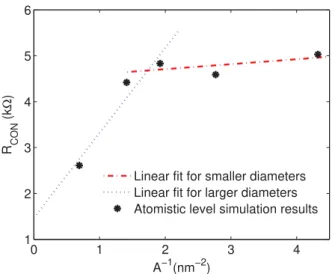
PtCl4 doping. . . 57 3.21 For MWCNT of diameter 7 nm, it is shown in the left Y-axis that
doping efficiency of Nc = 5 varies with defects and no contact resis-tance. With doping of Nc = 5, tolerated contact resistance to remain the total resistance unchanged for various defect scenarios is shown in the right Y-axis. Each tolerated contact resistance is derived with corresponding doping efficiency for each defect scenario. . . 59 3.22 Doping efficiency of MWCNT of diameter 7nm. Doping concentration
is fixed as Nc = 5. The presence of contact resistance decreases the doping efficiency for various defects concentration. . . 59 3.23 Theoretical prediction of linear resistance for a defective pure MWCNT
with contact resistances, similar conditions to the experimental mea-surements. 1000D means defects free and 10D represents highly de-fective. . . 60 3.24 50% of resistance improvement after doping with different Nc (red
line: Nc = 1; green line: Nc = 10). Resistance improvement has also dependence on contact resistance and defects related CNT mean free path. 1000D means defects free and 10D represents highly defective. . 60 4.1 (a) Cu electromigration: 1) Bulk EM, 2) Grain boundary EM, 3)
Grain/Bulk EM, 4) Defect EM, 5) Surface EM. (b) Performances of Cu-CNT composite from [144].. . . 66 4.2 Pure copper electrical-thermal modeling sketch. . . 70 4.3 Interconnect (includes Cu, CNT, and Cu-CNT) unit cell heat
con-duction self consistent simulation flow. . . 71 4.4 Pure Cu interconnect metal temperature profile for 7 nm node metal
level 2-3 with heat diffusion coefficient to the substrate (a) g = 0.1 W/m/K. (b) g = 0.2 W/m/K. (c) g = 0.3W/m/K. . . 72 4.5 Pure Cu interconnect metal temperature profile under various
electri-cal bias for 7 nm node metal level 4-6 with heat diffusion coefficient to the substrate (a) g = 0.1 W/m/K. (b) g = 0.2 W/m/K. (c) g = 0.3 W/m/K. . . 72 4.6 Pure Cu interconnect metal I-V variations under different heat
dif-fusion coefficient to the substrate for (a) Metal level 2-3. (b) Metal level 4-6. The unit of heat diffusion coefficient g is W/m/K. . . 73 4.7 Pure Cu interconnect metal Resistance variations under different heat
diffusion coefficient to the substrate for (a) Metal level 2-3. (b) Metal level 4-6. The unit of heat diffusion coefficient g is W/m/K . . . 73 4.8 Standalone CNT electrical-thermal modeling sketch. . . 74 4.9 SWCNT (D = 3 nm) interconnect temperature profile with heat
dif-fusion coefficient to the substrate (a) g = 0.1 W/m/K. (b) g = 0.2 W/m/K. (c) g = 0.3 W/m/K. . . 75
4.10 SWCNT interconnect (a) I-V variations (b) resistance variations un-der different heat diffusion coefficient g values (W/m/K) to the sub-strate. . . 75 4.11 MWCNT (D = 6 nm) interconnect temperature profile with heat
diffusion coefficient to the substrate (a) g = 0.1 W/m/K. (b) g = 0.2 W/m/K. (c) g = 0.3 W/m/K. . . 76 4.12 MWCNT (D = 6 nm) interconnect (a) I-V variations, (b) Resistance
variation under different heat diffusion coefficient g (W/m/K) to the substrate. . . 77 4.13 (a) Cu-CNT composite for global interconnects (b) Horizontally and
vertically aligned Cu-CNT composite for global interconnects. . . 77 4.14 Cu-CNT composite unit cell geometry sketch. . . 78 4.15 Cu-CNT composite unit cell electrical-thermal modeling sketch. . . . 78 4.16 SWCNT-Cu composite interconnect temperature profile. Dswcnt = 3nm,
and surrounding Cu dimensions are taken for 7 nm node metal level 2-3. Temperature variations under different heat diffusion coefficients to the substrate (a) g = 0.1 W/m/K. (b) g = 0.2 W/m/K. (c) g = 0.3 W/m/K. . . 80 4.17 SWCNT-Cu composite interconnect temperature profile.Dswcnt = 3nm,
and surrounding Cu dimensions are taken for 7 nm node metal level 4-6. Temperature variations under different heat diffusion coefficients to the substrate (a) g = 0.1 W/m/K. (b) g = 0.2 W/m/K. (c) g = 0.3 W/m/K. . . 80 4.18 SWCNT-Cu composite interconnect I-V variations under different
heat diffusion coefficient to the substrate for (a) surrounding Cu with dimension of metal level 2-3. (b) surrounding Cu with dimension of metal level 4-6. SWCNT with its diameter of 3 nm. The unit of heat diffusion g coefficient is W/m/K. . . 81 4.19 SWCNT-Cu composite interconnect Resistance variations under
dif-ferent heat diffusion coefficient to the substrate for (a) surrounding Cu with dimension of metal level 2-3. (b) surrounding Cu with di-mension of metal level 4-6. SWCNT with its diameter of 3 nm. The unit of heat diffusion g coefficient is W/m/K. . . 81 4.20 MWCNT-Cu composite interconnect temperature profiles. Dmwcnt = 6nm,
and surrounding Cu dimensions are taken for 7 nm node metal level 2-3. Temperature variations under different heat diffusion coefficients to the substrate (a) g = 0.1 W/m/K. (b) g = 0.2 W/m/K. (c) g = 0.3 W/m/K. . . 82 4.21 MWCNT-Cu composite interconnect temperature profiles. Dmwcnt = 6nm,
and surrounding Cu dimensions are taken for 7 nm node metal level 4-6. Temperature variations under different heat diffusion coefficients to the substrate (a) g = 0.1 W/m/K. (b) g = 0.2 W/m/K. (c) g = 0.3 W/m/K. . . 82
dimensions of metal level 2-3. (b) surrounding Cu with dimensions of metal level 4-6. MWCNT has a diameter of 6 nm. The unit of heat diffusion g coefficient is W/m/K. . . 83 4.23 MWCNT-Cu composite interconnect Resistance variations under
dif-ferent heat diffusion coefficients to the substrate for (a) surrounding Cu with dimensions of metal level 2-3. (b) surrounding Cu with di-mensions of metal level 4-6. MWCNT has diameter of 6 nm. The unit of heat diffusion g coefficient is W/m/K. . . 83 4.24 Ampacity vs. Conductivity [144]. . . 84
5.1 Illustration of end and side contact for CNT interconnect. . . 91 5.2 Sketch of CNTFET based Inverter - MWCNT Interconnect - Inverter. 92 5.3 Circuit level simulation schematic of Inverter - Interconnect - Inverter
for two testcases: CNTFET device + MWCNT line and FinFET
device + Cu line. . . . 92
5.4 MWCNT interconnect electrical compact model [29]. . . 93 5.5 (a) and (b) shows the number of conducting channels varies with Ef
shift for metallic and semiconductor shells with respect to different CNT diameters. . . 93 5.6 (a)-(d) are simulation results relating to Testcase A: CNT based
tech-nology. (a) represents energy delay product (EDP) as varying CNT-FET width (W) and tube to tube spacing (s) with ideal interconnects. (b) shows the circuit level EDP variation when including pristine MWCNT interconnect between CNTFET based Inverter 1 and In-verter 2. (c) shows the overall EDP variation with doped MWCNT interconnects (Ef shifts 0.3 eV) under different W and s. (d) illus-trates the overall circuit EDP improvement by introducing different doping to the MWCNT interconnects. . . 95 5.7 (a)-(c) are simulation analysis to compare carbon based technology
and advanced CMOS technology . (a) and (b) represent overall circuit level delay, power consumption for devices (CNTFET and FinFET) with ideal and realistic (doped MWCNT and Cu) interconnects re-spectively. (c) shows the circuit level energy delay product (EDP) for CNT tech and CMOS tech with different interconnect configurations. Pristine and heavily doped MWCNT interconnects are included for CNTFET devices; and for FinFET devices, Cu interconnects with various aspect ratio (A/R) are considered for comparison. . . 99 5.8 Energy delay product ratio between CNT tech and CMOS tech for
specified area A and B (in Fig. 5.7 (c)). (a) and (b) corresponds to area A and B respectively. MWCNT interconnect contact resistance and doping level are varied based on different given parameters (inset tables).. . . 100
5.9 Schematic of circuit gates connection of various interconnect scenarios including the MWCNT interconnect case (a), ideal interconnect case (b) and the copper interconnect case (c). . . 101 5.10 Corresponding Copper and CNT interconnect placement. . . 101 5.11 (a) Metal 1 pitch for different technology nodes from IRDS 2017.
(B) Prediction of resistivity of copper interconnect under different technology nodes according the IRDS 2017 and that from [2]. . . 102 5.12 Delay (a) and power (b) characterization results of a full-adder at
different technology nodes. The ratio of these two interconnects and its with technology nodes is also shown in (c). . . 103 5.13 Impact of doping on MWCNT interconnect performance at the
full-adder circuit level. Both total metallic CNT and CNT of 1/3 metallic chirality are concerned and compared with copper interconnect. The study case is at the 5 nm technology node. . . 104 5.14 Impact of CNT interconnect defects on the full-adder performance
(delay) under different Fermi levels or doping. Both 1/3 chirality MWCNT (a) and fully metallic MWCNT are shown (b). Power re-sults are similar changed and thus not shown here.. . . 104
List of Tables
1.1 Alternative interconnects for future technology node. . . 7 1.2 Main Contributions in this Thesis . . . 13 2.1 Values of pristine SWCNT Resistance for various length and diameter 20 3.1 Summary of Ef shift of double-wall CNTs (DWCNTs). Ef shift is
calculated based on the valence band edge [93]. . . 41 3.2 Representative Ef shifts for MWCNT with Dmax = 11 nm and the
NC for metallic (NCm) and semiconducting (NCs) CNT shells. Also shown are the ratios of metallic CNT shells at different Ef shifts. . . 46 3.3 Comparisons of doping efficiency in reducing MWCNT resistance
be-tween the all-sources simulation results and the experimental data in this work or that from [93]. . . 51 4.1 Width, thickness, and effective Cu resistivity values normalized to
the bulk resistivity of 1.8 µΩ·cm for interconnect layers at the 45-, 22-, 11-, and 7-nm technology nodes based on the Nangate open cell library interconnect stack and assuming a dimensional scaling factor of 0.7X at each new technology generation. [146] . . . 87 5.1 Experimental contact resistance realized with different contact
mate-rials and contact structure . . . 90 5.2 0.9Testcase II : FinFET + Cu interconnects . . . 97
Chapter 1
Introduction
1.1
Overview of On-Chip Interconnects
In today’s modern society, fast and efficient lifestyle requires rapid, accurate, and safe information exchange. Enormous information and data acquired through vari-ous electronic devices. Different activities rely on complex electronic networks and the internet. Smart city, internet of things (IoT), and artificial intelligence of things (AIoT) become the essential trend for future technology development. Super-speed neuromorphic and quantum computing indicate the prospects of taking over the Von Neumann architectures. However, all these developments and evolutions consume a huge amount of energy. Satisfying high-performance and at the same time ultra-low power are the center of the interest for the next generation technologies. In order to meet the demand of data abundant workloads and its energy efficiency, miniatur-ization of microelectronic products, more precisely, the transistors, with enhanced functionality and decreased cost open the possibility to meet the aforementioned requests.
Nevertheless, improving only the transistor performance of future chip isn’t suf-ficient. Chips are only one small part of the very large and complex information technology puzzle, albeit a very important one. Thus, to shape the future of the digital world, we also have to look at the bigger picture. Transistors are only as good as the system in which they are embedded. The fastest microprocessors are useless if the capacity of the data lines is not increased accordingly. This is where current electrical copper (Cu) interconnects will approach their physical limitations and may no longer be able to keep pace with a processor’s data throughput. In fact, the operation frequency of today’s CPUs is already governed by interconnect delays, and, during operation, most their power is dissipated in the interconnects. Therefore, the lack of improved interconnects is responsible for today’s trend to-wards merely size-scaling without concurrent performance scaling of CMOS, unlike previous decades of scaling.
On-chip interconnects include global, intermediate and local interconnects. In
Fig. 1.1 [1], it shows the on-chip interconnect structure. For global interconnects,
vias are used for signal and power delivery. Large amount of current passes through global interconnects can generate severe electromigration (EM) issues. Metals with low resistivity and being strong against electromigration effect become the priority
Figure 1.1: On-Chip hierarchical cross-sectional interconnect structure [1].
choices. Scaling of global interconnects is not as critical as intermediate and local interconnects. However, it still remains necessary to find solutions for electromigra-tion problem and interconnects reliability. Intermediate interconnects are the metal wires connecting between cells and cores/modules. The module complexity leads to a rapid increase of wire resistances and capacitances when we scale the intermediate interconnects. Air gaps can be used to reduce capacitance effects, but the increase of resistance is critical. Local interconnects are short connections between cells and are the most sensible interconnects to the transistor miniaturization. As transistors size shrinks and density increases, there requires a huge amount of local intercon-nect, thus wire congestion and resistance become detrimental for future technology nodes. New materials and components with barrier-less and ballistic transport are widely investigated.
On-chip delay becomes dominating by interconnects when the minimum on-chip
feature size scales to submicron region (Fig. 1.2). Accompanying with the
minia-turization of device feature size, intrinsic gate delay decreases while interconnect RC delay increases and becomes dominant for overall performance. Moore’s law
[110] indicates that on-chip transistors double its number for every two years in
order to meet the request for better performance and higher volume production. Due to the area limitation of the chip, integrating two times of transistors need to scale down each of them. Scaling of transistors increases their performances and further aims to improve the chip overall performance. However, the increase of the chip performance cannot be guaranteed if only devices are optimized but without interconnects. Therefore, exploring and investigating alternative on-chip intercon-nect conductor materials are critical for future high performance and energy efficient chips.
Chapter 1
Figure 1.2: Interconnect delay becomes dominant for submicron region [100].
1.2
Copper Interconnects
Accelerated technology scaling has aggravated Cooper (Cu) resistivity increase due to electron scattering and even more severely, it introduced electromigration issues. Mass transport along interfaces and grain boundaries in state-of-the-art Cu inter-connects is one of the most important issues to be solved for future technology nodes
according to the International Roadmap for Devices and Systems (IRDS) [2].
During several decades, aluminium (Al) has been used for on-chip interconnect wires. Due to the demands of wire scaling and lower wire resistivity, copper with its low resistivity, low cost and less oxidation than Aluminium and scalability has been considered for the suitable interconnect wires until nowadays. However, with the continuous downscaling of Cu interconnect linewidth, performance and reliability of interconnect conductors become severe issues to follow the transistors scaling. The advancement of thin metal wire photo-lithography is also an important factor for realization challenge, surface roughness increases with metal linewidth gets thinner. High current density will lead the interconnect material breakdown along the con-ducting path, which will further cause circuit malfunction and accelerate the chip’s time to failure. Two main issues of current Cu interconnects are 1) exponential increased resistivity and 2) occurrence of electromigration effect, which indicate the physical bottleneck of Cu interconnects for further performance improvement.
1.2.1
Copper Interconnects - Resistivity
For Cu interconnects structure, there are not only the metal conductor itself but accompanying with barrier layer to prevent Cu diffusion into the surrounding dielec-tric, nucleation layer on the barrier material to enable metal film growth, and then
metal conductor filling inside [143]. While interconnects are downscaled, thickness
electri-cal resistivity where rising of electron scattering at metal grain boundaries and at
metal surface and interfaces. Figure 1.3(a) illustrates the scattering phenomena for
an interconnect structure, and increase of Cu resistivity due to grain boundaries an scattering effects is shown in (b).
Other important factors are also contributing to the interconnect total resis-tance, such as the contact resistance and interconnects geometry. With shrinking of linewidth, contact resistance is increasing as contacting area is reduced, thus the overall interconnect performance degrades. Inter-metal capacitance is also governing the interconnect performance, which is geometry and inter-metal dielectric
depen-dent. Air gap [113] and low-k (dielectric constant) insulating materials are studied
recently in order to reduce the effective dielectric constant.
(a) Cu interconnect structure (b) Cu interconnect resistivity
Figure 1.3: (a) Copper interconnects suffer from grain boundary and surface scat-tering effects. (b) Grain boundary and scatscat-tering effects increase Cu interconnects
resistivity with shrinking of Cu width [77].
1.2.2
Copper Interconnects - Electromigration
Apart from increase of resistivity and degradation of performance, another critical metric for interconnects is the reliability, which determines how an interconnect con-ductor can maintain charge flow that goes through it without damaging the metal conductor and degrading performance, or even causing interconnect material break-down. Downscaling of interconnects indicates the reduction of wire cross-sectional
area and maximizing the current density J, in A/cm2 [97]. Once the maximum
current density approaches the conductor material current-carrying capacity, the moving electrons with associated electric field have enough energy to displace atoms from their original lattice sites where voids and hill-hocks can happen in the thin conductor material. This is due to a combination of the electron wind force, the temperature gradient induced force, the stress gradient induced force and the sur-face tension force. This phenomenon is known as electromigration (EM). EM is a
Chapter 1 severe issue leading the chip failure and malfunctions. The maximum current
den-sity projected for interconnects in future technology nodes is Jmax ≥ 2MA/cm2 [97]
from 2014 on. Cu bulk material maximum current-carrying capacity is 2MA/cm2,
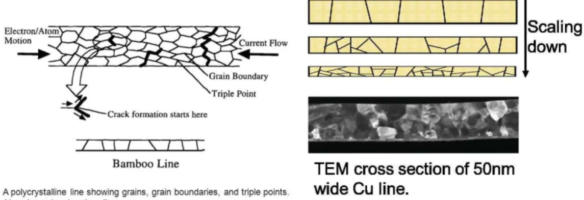
that clearly cannot meet the requirements for future technology nodes. In Fig. 1.4
(a), a polycrystalline line showing grains, grain boundaries and triple points and structure cracks happen at those interfaces are shown. TEM (Transmission Elec-tron Microscopy) image in (b) shows the cross section of 50 nm wide Cu line with EM issues. This material intrinsic property limitation shows the bottleneck of Cu for further on-chip interconnects implementation due to its severe reliability issue.
1.3
Emerging Interconnects for Advanced
Tech-nology Node
1.3.1
Metal Interconnects: Cobalt and Ruthenium
On-chip interconnects integration requires a Damascus process where Cu metal is surrounded by liner/barrier layers and then dielectrics. Existence of barrier layer of Cu interconnect trenches is necessary and can not be scaled less than certain thickness (∼2 nm). Hence the effective fraction of Cu lines is shrinking such that thin Cu lines with a barrier will induce an important resistance increase and perfor-mance degradation, and even more prone to electromigration (EM). Therefore, the alternative metals Ruthenium (Ru) and Cobalt (Co) are investigated to replace Cu with the same Damascus integration process. Even-though, Ru and Co have higher resistivity than Cu, but being barrierless makes the effective trench resistance less than that of Cu.
Recently, the major semiconductor industries have investigated alternative
met-als for advanced technology nodes. Table 1.1 summarizes the state-of-the-art
alter-(a) Polycrystalline line interconnect struc-ture
(b) Cu interconnect EM phenomenon under TEM observation
Figure 1.4: (a) Formation of electromigration for a bulk metal interconnect. (b) Scaling induced more electromigration effects, voids and breaks are dominant for Cu interconnects performance and lifetime.
native materials for future interconnects. For 14 nm node, Cu and W (tungsten)
[3, 182] are being investigated for process and barrier materials by Intel. Co will
be mainly explored by Intel and Global Foundries due to its barrierless advantages
[40, 154] for 10/7 nm nodes. Further scaling to 5/3 nm nodes, IMEC is stretching
out the possibility of Ru thanks to its weak thickness dependent resistivity [155,
40, 178, 4]. When technology node scales to beyond 3 nm, new materials need
to be explored. Such as carbon nanotube, graphene nanoribbon and other com-posite materials. TSMC is considering the carbon based materials, more precisely
multi-layered graphene nanoribbon [159]. Ballistic transport and high thermal and
electrical conductivity in carbon based materials and its composite indicate its suit-ability for interconnects, however, contact resistance and integration process are still big challenges.
C h ap te r 1 T ab le 1. 1: Al te rn at iv e in te rc on n ec ts fo r fu tu re te ch n ol og y n o d e. Technology 14nm 10/7nm 5/3nm <3nm Interconnect metals Cu / W [3, 182] Co [155,40, 154] Ru [155, 40,178,4] New compound: CNT, GNR [159,176], composite material [144]
Advantages Low resistivity No barrier Weak thickness
dependent resistivity Ballistic transport
Limitations Barrier effect High resistivity Surface scattering Integration / Contact resistance
Industries Intel Intel / Global Foundries IMEC TSMC
1.3.2
Graphene Nanoribbon Interconnects
Graphene has been discovered in 2004 [116]. Graphene is a monolayer hexagonal
lattice arrangement of carbon atoms. Due to its special nature of semi-metallic properties, where conduction band and valence band cross at Dirac point, its elec-trons behave like massless Dirac fermions that makes graphene having a high carrier velocity and current density. Hence, many researches on graphene are driven for elec-tronic devices and interconnects applications. A narrow stripe of graphene, known as graphene nanoribbon (GNR) has been investigated for promising candidate to
replace the transistor channels [11, 117] and interconnects [130] for next-generation
very large scale integrated (VLSI) circuit. GNR has many advantages on
electri-cal [107], mechanical [83] and thermal [10, 12] properties. GNR has high carrier
mobility and thermal conductivity [134]. The electron mean free path in GNR can
reach several micrometers [15] and its thermal conductivity is in the range of 5300
W/mK. However, GNR has metallic or semiconducting properties depending on the edge atoms arrangement. A zigzag-edged GNR behaves metallic and armchair-edged
GNR is semiconducting [112]. It still remains challenge to fabricate high quality and
fully metallic GNRs for large scale interconnect applications. However, due to the 2D quantization and narrow bandgap of semiconducting GNR, at room temperature or above, thermal effects induced electrons transition can make the narrow bandgap negligible. GNRs become one of the interesting and promising alternatives for future
on-chip interconnects applications [159, 176].
1.3.3
Carbon Nanotube Interconnects
Carbon nanotube (CNT) is discovered as multi-walled (MWCNT) in 1999 [63] by
Japanese researcher S. Iijima. Single-walled CNT (SWCNT) is discovered two years
after in 1993 [64, 17]. CNT can be seen as wrapping up one or multi graphene
sheets into a 1-dimension cylindrical wire, the inter-shell distance is defined by Van
der Waals distance (0.34 nm) [45, 46]. Diameter of SWCNT can vary from 0.4 nm
to 4 nm (typical diameter is ∼1.4 nm). The outermost shell diameter of MWCNT
can be up to 100 nm. CNT as 1-D quantum wire, has a very strong sp2 covalent
bonding between carbon atoms [166], hence having a very good electron confinement
in uni-axial-direction. CNTs also have unique physical properties that one third of
them are metallic and the rest are semiconducting depending on their chirality [165,
131].
Metallic CNTs have very good properties for interconnect applications, such as
ballistic transport [76,135,9], large electron mean free path (up to several µm) [164,
90,105,129,53,172,89, 5], high mechanical strength (∼1 TPa) [148, 132,88], high
ampacity (up to 109 A/cm2) [161, 171, 162] and high thermal conductivity (from
2000 W/mK to 7500 W/mK) [14, 21,66]. However, CNTs still have reliability
chal-lenges on fabrication process and design aspect. For the past decades, researchers
have investigated on low temperature [157,173,92], high density (>1013cm−2) [151,
44, 181, 118], high quality growth process. CNTs orientation control [151, 44, 145,
179,22,72] and high metal-CNT contact resistance [103,32,169,31] were also been
studied for nano- and micro- electronics applications. Nevertheless, chirality
Chapter 1 big challenge for silicon process compatible back-end-of-line (BEOL) integrations.
CNTs have been well investigated in the past thirty years. A brief history of
essential achievements of CNTs on electronic applications is shown in Fig. 1.5. Ten
years after the discovery of CNTs, IBM has demonstrated the possibility of CNT based transistor. Semiconducting CNT has been used as transistor channel under back-gated. One year after, in 2002, Kreupl from Infineon has first proposed CNTs with metallic properties for interconnect usage. In 2013, first CNT based computer
were demonstrated by Shulaker et al. in Stanford University [136]. With further
technology development, in 2015, 7 nm p-channel SWCNT based channel transistor using p-type end contacts are shown by IBM. In 2016, employing CNTs mechanical properties, the company NANTERO have developed a CNT based non-volatile ran-dom access memory (RAM) for molecular computing. In 2017, Stanford University built a CNT based chip by using three-dimensional integration of nanotechnologies
for computing and data storage [137]. This chip has integrated silicon logic,
CNT-FET logic, RRAM (resistive random access memory) and CNTCNT-FET based logic and sensors.
C
h
ap
Chapter 1
1.4
Structure of the Thesis
The focus of this thesis is to explore the potential of carbon nanotubes and car-bon nanotube composite for next generation energy efficient on-chip interconnects. Based on the state-of-the-art physical compact models for pristine SW and MW CNTs, we firstly developed models by taking into the account the doping effect, variability impacts, and thermal effect. Secondly, we explored doping of CNTs to indirectly control CNTs chirality uncertainty, enhance its conductivity, and miti-gate defects and high contact drawbacks. Our models are based on experimental grown low temperature CVD CNTs. Thirdly, we studied CNTs and CNT-Cu com-posite electrical-thermal properties for intermediate and global interconnects usage. Due to high current density, interconnects thermal effect (self-heating) is one of the main factor for electromigration issues and interconnect breakdown. Finally, we integrated our electrical models into circuit benchmarks in order to understand its performance and energy efficiency, in addition, comparing with Cu interconnects.
This thesis is part of and has been funded by European Commission H2020 CONNECT Project under Grant 688612. CONNECT project is a collaboration among University of Glasgow (UoG), UK; LIRMM-CNRS, France; CEA Leti/Liten, France; Fraunhofer (FhG), Dresden, Germany; Synopsys, UK; AIXTRON Ltd., Cambridge, UK; and IBM Switzerland.
This thesis is mainly working on compact modeling and circuit level simulations by taking inputs from fundamental atomistic level simulation results (UoG), and providing feedbacks to experimental partners (CEA and FhG) for experiment guid-ance and model validations. In addition, providing circuit level design guidelines for CNT based circuit.
This thesis is organized as follows:
• Chapter 2: Pristine Carbon Nanotube
In this chapter, we describe the pristine CNT electrical resistance (R) and capaci-tance (C) compact models based on literature works. We started by investigating basic pristine single-walled (SW) and multi-walled (MW) CNTs RC models. Fur-thermore, we performed a thorough study on process variations and their impact on MWCNT interconnect performance.
• Chapter 3: Doping of Carbon Nanotube
In this chapter, we evaluate MWCNT interconnects performance and variability while considering the impact of doping. We introduce a new parameter, the number
of conducting channels (NC) and incorporate it into our enhanced MWCNT compact
model described in Chapter 2. By theoretically calculating NC as a function of Fermi
level shift Ef - we evaluate each source of variation (diameter, chirality, defects) and
all-sources using Monte Carlo (MC) simulations. Simulation results are subsequently compared with experimental results, and a good consistency is found between them.
In this chapter, we started by investigating the electrical-thermal properties for Cu, SWCNT, MWCNT, SWCNT-Cu composite and MWCNT-Cu composite separately. We build electrical-thermal model for each of the cases by including self-heating, heat diffusion to substrate effects. A self consist heat conduction differential equation system is solved to extract temperature profile along the interconnect. In addition, we derived their I-V curves and resistance variations under various voltage supply. Ampacity is calculated in order to understand the material reliability. This study needs further validations with experimental data.
• Chapter 5: Circuit Level Analysis of Carbon Nanotube
Intercon-nects
In this chapter, we investigated circuit-level performance of doped MWCNT inter-connects and the potential of all carbon technology. we compared CNT based field effect transistor connecting by our standalone MWCNT interconnect (CNTFET +
MWCNT line) with FinFET connecting by conventional Cu interconnect (FinFET + Cu line) as two advanced technology testcases. CNTFET, 7nm FinFET and
PTM Cu interconnect models are used to perform circuit-level simulations. Over-all circuit delay, power and energy delay product are computed for both testcases. Furthermore, a full-adder benchmark is employed to study and compare different in-terconnect choices: ideal inin-terconnects, Cu inin-terconnects and standalone MWCNT interconnects.
• Conclusion and Perspective
In conclusion, we summarised the main achievements from each chapter and give takeaway key messages. We descried next steps and further investigation perspec-tives.
Chapter 1
Table 1.2: Main Contributions in this Thesis
Chapter Main Contributions Assessment
Chapter 2 1) We present a compact shell-level model
of MWCNT to include the defects, chiral-ity, end-contact resistance and shell con-nectivity to end-contacts. 2) We perform Monte Carlo (MC) or best/worst cases simulations to study variations in diam-eter, chirality, the presence of defects (de-fect density) and contacts.
We provide the first shell-to-shell MWCNT
distributed models
including variability
sources.
Chapter 3 We investigated doping of CNTs by
intro-ducing Fermi-Level shift related number of conducting channels Nc as physical key parameter for doped CNT models. 1)
An-alytical calculations of NC vs. EF shift. 2)
Enhanced doped CNT electrical compact models and simulations. 3) Experimental results correlation and comparison.
For the first time, a
systematic
investiga-tions are realized by
including theoretical
modeling and
experi-mental measurements
for doped standalone
CNT interconnect.
Good consistency is
found between them.
Chapter 4 1) We investigated the electro-thermal
properties and modeling on SW/MW CNTs and CNT-Cu composite. 2) Tem-perature profile, I-V and resistance varia-tions are evaluated based on our electro-thermal models. 3) CNT-Cu composite ampacity and conductivity are extracted for state-of-the-art results comparison.
A macroscopic physical
based electro-thermal
model for CNT-Cu com-posite for interconnects. We explored for the first time compact modeling of CNT-Cu composite
for intermediate and
global interconnects.
Chapter 5 1) We investigated circuit-level
bench-marking and simulations for all carbon based circuit (CNTFET + CNT lines), and comparing to conventional Cu tech-nology. 2) Full-adder circuit is employed to evaluate the performance and energy of CNT interconnects.
We evaluated our mod-els in circuit-level to provide useful insights for future CNT inter-connect design guide-line.
Chapter 2
Pristine Carbon Nanotubes
2.1
Introduction
As technology scales down, the transistor performance continues to improve. How-ever, for interconnect, scaling leads to higher current density and more substantial resistance. The transition of interconnect material from Aluminum (Al) to Copper (Cu) a few decades ago enabled further scaling of interconnects. Nevertheless, Cu interconnects resistance rises rapidly as its dimensions scale and become
compa-rable to the order of electron mean free path (∼40 nm at room temperature) [65],
[143]. Compared with Cu, carbon nanotube (CNT) has attractive properties such as
ballistic transport, high thermal conductivity, and ampacity [146],[98]. Because of
strong sp2 bonding between carbon atoms, CNT is much more resistant to
electro-migration (EM) and can sustain significantly larger current densities than Cu [162].
Furthermore, self-heating problem is a concern on deeply scaled Cu interconnects whereas CNTs have long ballistic electronic transport length ∼1 µm, making them have higher electrical and thermal conductivities and thus capable of carrying high
current density with virtually no heating thanks to its 1D electronic structure [147,
13, 57].
Carbon nanotubes are currently being investigated as potential replacement of back-end-of-line interconnect copper material for integrated circuits. Carbon nan-otubes have a semiconducting or metallic property due to their special Dirac energy band structure and open a field for nano- or micro-electronic devices and inter-connect applications. Compared with Cu line process, the fabrication of CNT
re-quires different processing steps and much higher temperature (up to 900oC [121])
to achieve good quality CNT growth. However, achieving back-end-of-line process compatible with CNTs would require to grow them at a lower temperature such as
450oC to 500oC. Growing CNTs at such temperatures introduces several variations,
i.e., diameter, chirality. Furthermore, at such temperatures defects are omnipresent, and the most typical types are vacancies, interstitials, non-hexagonal rings and grain
boundaries [38], [177]. Defects can trap or scatter carriers and thus ultimately
im-pact CNT interconnect performance.
Good contacts between the CNTs and metal electrodes are very challenging. Poor contacts induce a significant contact resistance or might be even disconnected
concern for vertical interconnects where the electrode acts as a support for the
catalytic growth of CNT and also as an electrical contact [50]. Currently, there
are two types of contacts with CNTs - side-contacts and end-contacts [23]. The
side-contact has the metal deposited on top of the CNT, enabling the electrons to flow along the length of the metal-CNT tube interface and the contact resistance depends on the overlap length between the metal and CNT tube. End-contacts are formed between the end of CNT tube and metal. The interface between electrode and CNT for the end-contact is covalent metal-carbon bonds while it is Van der
Waals bond for the side contact as discussed and described in [23]. As a result, the
end-contact tends to have smaller contact resistance than the side-contact. Whereas, end-contacts in MWCNT may suffer from disconnected shells to the electrodes which ultimately also increases the contact resistance.
In this chapter, we describe the pristine CNT electrical resistance (R) and ca-pacitance (C) compact models based on literature works. We would like to start our work with a solid base by investigating basic pristine single-walled (SW) and multi-walled (MW) CNTs RC models. Furthermore, we perform a thorough study on process variations and their impact on MWCNT interconnect performance.
We investigate the CNT quantum transport property and use the number of
conducting channels NC as a figure of merit for computing the change in CNT
con-ductance due to process variations. On SWCNTs (with the diameter less than 10 nm) the variations in diameter have been shown to have little impact on its
con-ductance [91]. However, on MWCNTs, the diameter variations may change the
total number of shells and NC; thus, the MWCNT conductance can vary
signifi-cantly. Chirality determines the property of the CNT, which can be either metallic or semiconducting. Metallic and semiconducting CNT conductivities are
signifi-cantly different, especially for small diameter CNT [111]. Shell connection to the
end-contact also impacts overall MWCNT resistance, and even more so for MWCNT
with many shells [89].
To understand how CNT interconnect performance is impacted by these varia-tions, we develop a compact shell-level model capable of combining the MWCNT physical properties with process variations. Such a model is essential for circuit-level simulation and circuit design space exploration with MWCNT interconnects.
The contents in this Chapter have been published on:
[96]: Jie Liang et al. ”Physical description and analysis of doped carbon
nanotube interconnects”, in IEEE International Workshop on Power and Timing Modeling, Optimization and Simulations (PATMOS) (2016), pp. 250-255.
[29]: Rongmei Chen, Jie Liang , et al. ”Variability Study of MWCNT
Lo-cal Interconnects Considering Defects and Contact Resistances - Part I: Pristine MWCNT”, in IEEE Transactions on Electron Devices 65.11 (2018), pp. 4955-4962.
2.2
Physical Description of Carbon Nanotube
Carbon nanotube, known as 1-D quantum material which can be obtained by rolling up a mono-layered graphene sheet. Rolling direction of graphene impacts directly the physical properties of carbon nanotube. For a graphene mono-layered sheet,
Chapter 2
we define two unit vectors ~a1 and ~a2 that represent the minimum unit cell vectors
based on material crystallography physics. From vectors ~a1 and ~a2, we define the
carbon nanotube chiral vector ~C = n ~a1+ m ~a2, which indicates the graphene rolling
direction. Different n and m indices will provide a kind of rolling thus a type of carbon nanotube. There are typically three types of chirality for carbon nanotube:
chiral, zigzag and armchair. As shown in Fig. 2.1, chiral nanotube has the end sides
with unregulated shapes. For nanotubes having end sides shaped as zigzag form are named zigzag nanotube. And for armchair tubes, the end sides have flat up and down shapes, so called armchair. Carbon nanotubes are not only single walled (SW) but also multi walled (MW). For multi-walled carbon nanotube (MWCNT), there are coaxial single shell nanotubes formed together with different diameters as shown
in Fig. 2.2. Shell to shell distance is 0.34 nm, so called Van der waals distance.
Each shell of MWCNT has different chirality, thus different electrical properties. Therefore, a SWCNT or MWCNT is formed with various sources of variability that can impact nanotubes electrical properties. Impacts of different sources of variability are studied separately in the following sections of this chapter.
Figure 2.1: Carbon nanotube, based on different rolling direction, can have three types of chirality: chiral, armchair and zigzag. Chirality of carbon nanotube is
defined by chiral vector ~C which composed by indices n, m and unit vector ~a1 and
~ a2.
Beside defining carbon nanotubes by different chirality, we can as well define them by different electrical properties, either metallic or semiconductor nanotubes. Important parameters to define the metallic or semiconductor properties are given by chiral vectors indices n and m. If the difference (n-m) between n and m is a multiple of 3 and n6=m and nm6=0, then this type of carbon nanotube has a
Figure 2.2: Carbon nanotubes can be formed as single-walled (SWCNT) or multi-walled (MWCNT). MWCNT can be seen as coaxial SWCNT shells with different diameters.
quasi metallic property with bandgap nearly 0. Otherwise, nanotube is a moderate
semiconductor tube [79]. In Fig. 2.3, it illustrates the typical energy band structure
of metallic and semiconductor carbon nanotubes, where in (a), a Dirac point band structure is shown for metallic nanotube, and a clear bandgap is observed in (b) for semiconductor nanotube.
Another interesting properties of carbon nanotube is the diameter dependent electrical property. As the carbon nanotube diameter increases, tube metallic prop-erties increases, and large diameter MWCNT often shows a metallic property.
Figure 2.3: Typical Energy Band Structure of (a) metallic and (b) semiconductor carbon nanotube.
![Figure 1.1: On-Chip hierarchical cross-sectional interconnect structure [1].](https://thumb-eu.123doks.com/thumbv2/123doknet/7724671.248749/29.892.136.766.132.500/figure-on-chip-hierarchical-cross-sectional-interconnect-structure.webp)
![Figure 1.2: Interconnect delay becomes dominant for submicron region [100].](https://thumb-eu.123doks.com/thumbv2/123doknet/7724671.248749/30.892.286.607.137.447/figure-interconnect-delay-dominant-submicron-region.webp)
![Figure 2.9: Enhanced distributed p-shell MWCNT compact model proposed in this chapter based on the original compact model by [91]](https://thumb-eu.123doks.com/thumbv2/123doknet/7724671.248749/53.892.137.761.155.391/figure-enhanced-distributed-compact-proposed-chapter-original-compact.webp)