HAL Id: hal-02893580
https://hal.univ-lorraine.fr/hal-02893580
Submitted on 8 Jul 2020
HAL is a multi-disciplinary open access
archive for the deposit and dissemination of
sci-L’archive ouverte pluridisciplinaire HAL, est
destinée au dépôt et à la diffusion de documents
Optoelectronic domain-wall motion for logic computing
Boyu Zhang, Daoqian Zhu, Yong Xu, Xiaoyang Lin, Michel Hehn, Grégory
Malinowski, Weisheng Zhao, Stéphane Mangin
To cite this version:
Boyu Zhang, Daoqian Zhu, Yong Xu, Xiaoyang Lin, Michel Hehn, et al.. Optoelectronic domain-wall
motion for logic computing. Applied Physics Letters, American Institute of Physics, 2020, 116 (25),
pp.252403. �10.1063/5.0013369�. �hal-02893580�
Optoelectronic domain-wall motion for logic computing
Boyu Zhang,1 Daoqian Zhu,2 Yong Xu,2 Xiaoyang Lin,2 Michel Hehn,1 Gregory
Malinowski,1 Weisheng Zhao,2,a) and Stéphane Mangin.1,a)
1Université de Lorraine, CNRS, IJL, F-54000 Nancy, France
2Fert Beijing Institute, BDBC, School of Microelectronics, Beihang University, Beijing 100191, China
Abstract
Logic computing in magnetic domain walls is investigated using the interplay of all-optical helicity-dependent switching and current-induced spin-orbit torque switching. By simultaneously controlling current and laser pulses, logic functions of AND, OR, NAND and NOR are experimentally demonstrated through anomalous Hall effect and verified by micromagnetic simulations. The optoelectronic domain-wall motion is energy-efficient compared to the traditional all-current approach and provides another degree of freedom for the realization of logic applications.
Magnetic logic has the advantage of non-volatility and scalability and can execute different
logic gate operations.1-6 The dynamics of domain-wall (DW) motion has become a research
focus for its potential applications in high density magnetic memory and logic devices, where data are stored non-volatilely in the form of magnetic domains separated by DWs along
magnetic wires.7-9 Magnetic DW logic gates were first realized using a rotating-field-induced
DW motion in sub-micro magnetic wires, including NOT, AND, fan-out and cross-over
elements.1 As the external magnetic field limited their implementation, all-current chiral DW
motion based on spin-orbit torque (SOT) was exploited for magnetic logic.6 However, the
power consumption for DW logic operation is still relatively high. Recently, several logic
structures based on laser pulses have been proposed.10-11 All-optical switching (AOS) has the
advantages of faster writing speed and lower power consumption,12-14 which can be an
alternative approach for the realization of advanced magnetic logic devices.15-16 In this letter,
a)
Authors to whom correspondence should be addressed. Electronic mail: [email protected] and [email protected]
we demonstrate DW logic computing combining all-optical helicity-dependent switching (AO-HDS) and current-induced SOT switching. Four logic functions are realized and the physical origin is elucidated by micromagnetic simulations. Our findings provide additional insights toward energy-efficient optical-spintronic logic computing.
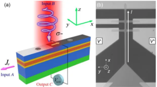
The samples were grown by magnetron sputtering on a glass substrate. The stack consists of a Ta(3 nm)/Pt(5 nm)/Co(0.3 nm)/Ni(0.6 nm)/Co(0.3 nm)/Pt (2 nm) thin film [Fig. 1(a)]. The
samples show a strong perpendicular magnetic anisotropy (PMA) with a coercivity field Hc of
3.5 mT. The structure is mainly composed of a 4-μm wire and Ti/Au contacts on each wire end for electrical current injection and Hall voltage detection [Fig. 1(b)].
FIG. 1. (a) Schematic of the optoelectronic DW motion structure for logic computing; (b) The microscope image of the 4-μm wire and the schematic illustration of the anomalous Hall effect (AHE) experimental geometry.
The input A is a pulse current injected from the triangle pad along x direction with a 10-μs pulse duration. After a DW nucleation in the wire, as the DW is Neel type due to the presence
of the Dzyaloshinskii-Moriya interaction (DMI) with DMI field HDMI of 300 Oe, it can be
moved against the electron flow Je, induced by SOT thanks to the asymmetric Pt layers. The
input B is a shined left-circularly (σ−) or right-circularly (σ+) polarized laser beam (40-fs pulse duration, 800-nm wavelength, 60-μm FWHM, 8 μm away from the initial DW position), which can generate AO-HDS on the wire. They are synchronized at a 5-kHz-repetition rate. A laser
fluence FLaser lower than 4.5 mJ/cm2 is not sufficient to move the DW and a SOT current density
JSOT lower than 15 MA/cm2 cannot move the DW neither. Those quantities define the threshold
values for JSOT and FLaser. After the inputs, the local magnetization can be detected via
anomalous Hall effect (AHE), which defines the output C.
Fig. 2 shows the experimental demonstration of the “AND”, “OR”, “NAND” and “NOR” logic gates via the optoelectronic DW motion. First, the magnetic wire is initialized to a magnetization pointing downwards (M↓) corresponding to a resistance state R “0” for (a) and (b), and to an upward direction (M↑) corresponding to a resistance state R “1” for (c) and (d). Next, a DW is nucleated, where its position is shown by the white dashed line in Fig. 2. The
inputs A and B are then applied during 10 s to operate the wire, where the values of JSOT and
FLaser are indicated in TABLE I and TABLE II. The laser helicity is σ+ for (a) and (b) and σ−
for (c) and (d), as σ+ or σ− favors M↑ or M↓ due to AO-HDS, respectively. It is noted that 4
mJ/cm2 linearly-polarized laser pulses with 7.3 MA/cm2 current pulses favor a shorter DW
motion toward the hottest region around the beam center compared to the one with σ+ or σ− (not shown), which is due to Gaussian distribution of the laser beam intensity and shows the
laser helicity contribution in the DW motion. The laser fluence FLaser is a space-dependent
function that follows the Gaussian distribution. Therefore, the DW motion is induced only in
certain areas with the laser fluence FLaser above the threshold value. Finally, the logic values of
resistance state R are readout at the output C (normalized Hall voltage 𝑉̅̅̅̅̅). Hall
JSOT and FLaser are below the threshold values of DW motion for (a) and (c), and the DW
propagates only when both inputs A and B are applied. Depending on the initial magnetic state,
(a) results in a “AND” gate and (c) results in a “NAND” gate. JSOT and FLaser are above the
threshold values of DW motion for (b) and (d), and the DW propagates when either input A or B is applied. Depending on the initial magnetic state, (b) results in a “OR” gate and (d) results in a “NOR” gate. The respective Kerr images of the magnetic contrast, obtained by subtracting
two images before and after the inputs, are also shown in the insets, where the black and white contrasts correspond to a reversal to M↑ and M↓, respectively. The operations are repeated and the above conclusions are confirmed.
For the implementation of optoelectronic DW logic gates into circuits, an electro-optic modulator (EOM) can be used to adjust the laser fluence by an electrical signal, which results in the same form of input and output that meets the concatenability requirement of logic
applications.17 By interconnection of multiple logic gates, more complicated logic functions
can be realized in a similar way.
TABLE 1. Values ofJSOT (input A) and FLaser (input B) for
respective operations in Fig. 2 (a) and (c). Input A: JSOT
(MA/cm2
) 0 7.3 0 7.3 Input B: FLaser
(mJ/cm2) 0 0 4 4
TABLE II. Values ofJSOT (input A) and FLaser (input B) for
respective operations in Fig. 2 (b) and (d). Input A: JSOT (MA/cm2 ) 0 16 0 16 Input B: FLaser (mJ/cm2) 0 0 5.4 5.4
FIG. 2. Experimental demonstration of the logic computing functions via the optoelectronic DW motion; (a) “AND”, (b) “OR”, (c) “NAND”, and (d) “NOR”.
To quantify the energy consumption, considering the same consumption during the DW
nucleation, the joint effect of laser pulses (FLaser = 4 mJ/cm2) and current pulses (JSOT = 7.3
MA/cm2) in Fig. 2(a) enables a DW displacement of 23.6 μm with a consumption of 4.2×10⁻⁴
J/μm, which is energy-efficient compared to the current-induced DW motion (JSOT = 16
MA/cm2) of 41.2 μm in Fig. 2(b) with a consumption of 7.8×10⁻⁴ J/μm. In addition, by replacing
the input B of laser pulses with current pulses (JSOT=7.3 MA/cm2 for Flaser=4 mJ/cm2 and
JSOT=16 MA/cm2 for F
laser=5.4 mJ/cm2), the pure current-induced DW logic operations of
“AND” and “OR” consume 50% more than the “AND” and “OR” operations of optoelectronic DW logic in our device. It is noted that the energy consumption during the magnetization initialization process is negligible compared to the logic operation process, because with proper laser fluence and pulse duration, an all-optical fully switched magnetic domain could be
realized by several hundreds of laser pulses in the laser-shining position of the wire.18 Therefore,
the proposed optoelectronic DW logic is also energy-efficient compared to the pure current-induced DW logic in our device, considering the similar energy consumption between “AND”, “OR” and “NAND”, “NOR”.
The physical origin of the optoelectronic DW motion for logic computing, which is
implemented by controlling JSOT and FLaser, is studied through micromagnetic simulations using
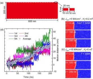
MuMax3.19 Fig. 3(a) exhibits the top view of the simulated ferromagnetic (FM) layer, with a
600-nm length and a 200-nm width. Periodic notches are distributed along the horizontal edges to provide the pinning force during the DW motion. Adopting the notch size presented in Fig.
3(a), the depinning JSOT used in the simulations (15 MA/cm2) is the same as the JSOT threshold
value in the experiments. The FM layer is regularly shaped to 4×4×1 nm3 rectangular grids.
The magnetization dynamics in each grid is calculated using the Landau-Lifshitz-Gilbert (LLG)
equation:20
𝜕𝒎 𝜕𝑡 = −𝛾𝜇0(𝒎 × 𝑯eff) + 𝛼 (𝒎 × 𝜕𝒎 𝜕𝑡) + 𝛾𝐽SOT𝜃SHℏ 2𝑒𝑡F𝑀s (𝒎 × 𝝈 × 𝒎) (1)
where Heff is the effective magnetic field with contributions from the uniaxial anisotropy field,
the demagnetization field, the exchange field, the DMI field, the laser-helicity-induced
perpendicular field Hz, and the fluctuating thermal field which is proportional to the square
root of the sample temperature T.19 m = M/M
s is the reduced magnetization and σ is the spin
polarization direction of SOT that originates from the Pt layer under the FM layer. α is the
Gilbert damping constant, γ is the gyromagnetic ratio, μ0 is the vacuum permeability, e is the
elementary charge, tF is the thickness of the FM layer, ћ is the reduced Planck constant, θSH is
the spin Hall angle. Unless specified, the material parameters used are given by the
experimental values: Ms = 770 kA/m, tF = 1.2 nm, θSH = 0.07, α = 0.1, anisotropy energy density
Ku = 6.25×10⁵ J/m3, exchange stiffness A = 15 pJ/m, DMI strength D = 0.2 mJ/m2. When no
laser pulse is applied, T is set to 300 K.
FIG. 3. Micromagnetic simulations of DW motion driven by the SOT current and laser excitation. (a) Schematic of the
simulated FM layer. Snapshots of z component of the magnetization at selected times when (b) JSOT = 5 MA/cm2, Hz = 0.2
mT and T+ΔT = 320 K and (c) JSOT = 15 MA/cm2, Hz = 0 mT and T = 300 K. (d) DW position as a function of time in 5
repeated simulations using the same parameters as in (b).
To investigate the influence of JSOT and FLaser on the DW motion, we initialize a DW at t = 0
ns and then record the DW position change under different external excitations until t = 200 ns. During this period, the laser effect gives a sample temperature increase ΔT that facilitates DW depinning, while the temperature increase due to current injection is negligible compared to
ΔT from laser shining.21 The reduction of some magnetic parameters upon increasing
temperature,22 which will contribute to a larger domain-wall depinning probability and motion
velocity, is not included in our simulations. But we note that overall functionalities that we demonstrated in this work remain valid though the required laser fluence or SOT current density could be lower. Fig. 3(b) shows the snapshots of the z component of the magnetization
at selected times when JSOT = 5 MA/cm2, Hz = 0.2 mT and T+ΔT = 320 K, which corresponds
to the values below the threshold. The DW moves 33.7 nm under the joint effect of SOT current injection and laser excitation. In contrast, the DW will mainly remain pinned when only one type of the above excitation is exerted (not shown). Therefore, by detecting the local magnetization state away from the initial DW position, the AND logic function is achieved
using JSOT = 5 MA/cm2 and FLaser below the threshold value as two inputs. The DW can also
be depinned when increasing JSOT and FLaser. Fig. 3(c) displays the DW motion driven only by
JSOT of 15 MA/cm2 above the threshold at T = 300 K, i.e., no laser pulse is applied. Similarly,
the DW can escape from the pinning sites when only laser pulses with fluence above the
threshold value shine (Hz = 1 mT and T+ΔT = 380 K). As a consequence, JSOT = 15 MA/cm2
and a FLaser above the threshold value can serve as the inputs of an OR logic gate. Since the
DW depinning process is probabilistic at a finite temperature, for each stimulus, we performed 5 repeated simulations with different random seeds. Fig. 3(d) shows the respective 5 simulations of DW position as a function of time using the same parameters as in Fig. 3(b). The average motion distance and standard deviation are summarized in Table III and Table IV.
TABLE III. Micromagnetic simulation results of DW motion in the AND logic gates.
Inputs (A,B) Current: JSOT
(MA/cm2) Laser: T+ΔT (K) Laser: Hz (mT) Motion (nm) Output R (0,0) 0 300 0 1.55±5.66 0 (1,0) 5 300 0 2.45±5.90 0 (0,1) 0 320 0.2 18.7±15.0 0 (1,1) 5 320 0.2 33.7±10.3 1
TABLE IV. Micromagnetic simulation results of DW motion in the OR logic gates.
Inputs (A,B) Current: JSOT
(MA/cm2) Laser: T+ΔT (K) Laser: Hz (mT) Motion (nm) Output R (0,0) 0 300 0 1.55±5.66 0 (1,0) 15 300 0 57.5±17.3 1 (0,1) 0 380 1 44.3±17.5 1 (1,1) 15 380 1 277±53 1
Thus, the above micromagnetic simulation results, which provide numerical estimations of the DW displacement, suggest “AND” gate for inputs below the threshold values and “OR” gate for inputs above the threshold values, and demonstrate the contributions of SOT, laser-helicity-induced effective field and sample temperature increase in the realization of logic computing functionality.
To summarize, we have demonstrated DW logic computing by synchronizing injected current and shined laser pulses on a Co/Ni/Co wire. The interplay of AO-HDS and current-induced SOT switching offers another degree of freedom to realize logic functions and the assistance of laser pulses in the current-induced DW motion reduces the energy consumption. Logic gates of AND, OR, NAND and NOR are experimentally realized and verified by micromagnetic simulations. Moreover, the downsizing of the AOS could be done using plasmonic antenna which is employed in heat assisted magnetic recording (HAMR) for hard drive, thus reducing
the FWHM of laser spot below 40 nm.23 Therefore, our proof-of-concept highlights an
alternative path toward energy-efficient optoelectronic logic applications.
This work was supported by the ANR-15-CE24-0009 UMAMI, by the Institut Carnot ICEEL for the project “Optic-switch” and Matelas, by the Région Grand Est, by the Metropole Grand Nancy, by the impact project LUE-N4S, part of the French PIA project “Lorraine Université
d’Excellence”, reference ANR-15-IDEX-04-LUE, and by the “FEDER-FSE Lorraine et Massif Vosges 2014-2020”, a European Union Program. The authors gratefully acknowledge the National Natural Science Foundation of China (Grants No. 61627813 and No. 51602013), the Program of Introducing Talents of Discipline to Universities (Grant No. B16001), the National Key Technology Program of China (Grant No. 2017ZX01032101), and the Young Elite Scientists Sponsorship Program by CAST (Grant No. 2018QNRC001).
The data that support the findings of this study are available from the corresponding author upon reasonable request.
References
1. D. A. Allwood, G. Xiong, C. C. Faulkner, D. Atkinson, D. Petit, and R. P. Cowburn, Science 309(5741), 1688-1692 (2005).
2. J. H. Franken, H. J. M. Swagten, and B. Koopmans, Nat. Nanotechnol. 7(8), 499-503 (2012).
3. R. Lavrijsen, J.-H. Lee, A. Fernández-Pacheco, D. Petit, R. Mansell, and R. P. Cowburn, Nature 493(7434), 647–650 (2013).
4. D. M. Bromberg, M. T. Moneck, V. M. Sokalski, J. Zhu, L. Pileggi, and J.-G. Zhu,in 2014 International
Electron Device Meeting, San Francisco, CA, USA, 15-17 December 2014 (IEEE, 2014), pp. 33.1.1-33.1.4. 5. J. A. Currivan-Incorvia, S. Siddiqui, S. Dutta, E. R. Evarts, J. Zhang, D. Bono, C. A. Ross, and M. A. Baldo,
Nat. Commun. 7(1), 10275 (2016).
6. Z. Luo, A. Hrabec, T. P. Dao, G. Sala, S. Finizio, J. Feng, S. Mayr, J. Raabe, P. Gambardella, and L. J. Heyderman, Nature 579(7798), 214-218 (2020).
7. S. Parkin and S.-H. Yang, Nat. Nanotechnol. 10(3), 195–198 (2015).
8. L. Caretta, M. Mann, F. Büttner, K. Ueda, B. Pfau, C. M. Günther, P. Hessing, A. Churikova, C. Klose, M. Schneider, D. Engel, C. Marcus, D. Bono, K. Bagschik, S. Eisebitt, and G. S. D. Beach, Nat. Nanotechnol.
13(12), 1154-1160 (2018).
9. X. Zhao, B. Zhang, N. Vernier, X. Zhang, M. Sall, T. Xing, L. H. Diez, C. Hepburn, L. Wang, G. Durin, A. Casiraghi, M. Belmeguenai, Y. Roussigné, A. Stashkevich, S. M. Chérif, J. Langer, B. Ocker, S. Jaiswal, G. Jakob, M. Kläui, W. Zhao, and D. Ravelosona, Appl. Phys. Lett. 115(12), 122404 (2019).
10.C. Ríos, N. Youngblood, Z. Cheng, M. Le Gallo, W. H. P. Pernice, C. D. Wright, A. Sebastian, and H. Bhaskaran, Sci. Adv. 5(2), eaau5759 (2019).
11.A. Chakravarty, J. H. Mentink, C. S. Davies, K. T. Yamada, A. V. Kimel, and T. Rasing, Appl. Phys. Lett.
114(19), 192407 (2019).
12.S. Alebrand, M. Gottwald, M. Hehn, D. Steil, M. Cinchetti, D. Lacour, E. E. Fullerton, M. Aeschlimann, and S. Mangin, Appl. Phys. Lett. 101(16), 162408 (2012).
13.S. Mangin, M. Gottwald, C. H. Lambert, D. Steil, V. Uhlíř, L. Pang, M. Hehn, S. Alebrand, M. Cinchetti, G. Malinowski, Y. Fainman, M. Aeschlimann, and E. E. Fullerton, Nat. Mater. 13(3), 286–292 (2014). 14.M. S. El Hadri, P. Pirro, C. H. Lambert, N. Bergeard, S. Petit-Watelot, M. Hehn, G. Malinowski, F.
Montaigne, Y. Quessab, R. Medapalli, E. E. Fullerton, and S. Mangin, Appl. Phys. Lett. 108(9), 092405 (2016).
15.M. L. M. Lalieu, R. Lavrijsen, and B. Koopmans, Nat. Commun. 10(1), 110 (2019).
16.A. V. Kimel, A. M. Kalashnikova, A. Pogrebna, and A. K. Zvezdin, Phys. Rep. 852, 1-46 (2020). 17.X. Lin, W. Yang, K. L. Wang, and W. Zhao, Nat. Electron. 2(7), 274–283 (2019).
18. G. Kichin, M. Hehn, J. Gorchon, G. Malinowski, J. Hohlfeld, S. Mangin, Phys. Rev. Appl. 12(2), 024019 (2019).
19.A. Vansteenkiste, J. Leliaert, M. Dvornik, M. Helsen, F. Garcia-Sanchez, and B. Van Waeyenberge, AIP Adv.
4(10), 107133 (2014).
20.J. Sampaio, V. Cros, S. Rohart, A. Thiaville, and A. Fert, Nat. Nanotechnol. 8(11), 839–844 (2013). 21.J. Curiale, A. Lemaître, G. Faini, and V. Jeudy, Appl. Phys. Lett. 97(24), 243505 (2010).
22.E. Grimaldi, V. Krizakova, G. Sala, F. Yasin, S. Couet, G. Kar, K. Garello, and P. Gambardella, Nat. Nanotechnol. 15, 111-117 (2020).
23.B. C. Stipe, T. C. Strand, C. C. Poon, H. Balamane, T. D. Boone, J. A. Katine, J.-L. Li, V. Rawat, H. Nemoto, A. Hirotsune, O. Hellwig, R. Ruiz, E. Dobisz, D. S. Kercher, N. Robertson, T. R. Albrecht and B. D. Terris, Nat. Photonics 4(7), 484-488 (2010).