HAL Id: tel-01124029
https://tel.archives-ouvertes.fr/tel-01124029
Submitted on 6 Mar 2015HAL is a multi-disciplinary open access archive for the deposit and dissemination of sci-entific research documents, whether they are pub-lished or not. The documents may come from teaching and research institutions in France or
L’archive ouverte pluridisciplinaire HAL, est destinée au dépôt et à la diffusion de documents scientifiques de niveau recherche, publiés ou non, émanant des établissements d’enseignement et de recherche français ou étrangers, des laboratoires
Croissance de nanostructures de composés III-nitrures
en épitaxie en phase vapeur d’organo-métalliques : de la
croissance auto-assemblée à la croissance sélective
Xiaojun Chen
To cite this version:
Xiaojun Chen. Croissance de nanostructures de composés III-nitrures en épitaxie en phase vapeur d’organo-métalliques : de la croissance auto-assemblée à la croissance sélective. Physique [physics]. Université de Grenoble, 2011. Français. �NNT : 2011GRENY080�. �tel-01124029�
THÈSE
Pour obtenir le grade de
DOCTEUR DE L’UNIVERSITÉ DE GRENOBLE
Spécialité : Nanophysique
Arrêté ministériel : 27 Octobre 2008
Présentée par
Xiaojun CHEN
Thèse dirigée par Jöel EYMERY et Codirigée par Christophe DURAND
préparée au sein du laboratoire Nanophysique et
Semi-conducteurs, CNRS/CEA/UJF-Grenoble I
dans l'École Doctorale de Physique de Grenoble
MOVPE growth of III-nitride
nanostructures : From
self-assembled growth to selective
area growth
Thèse soutenue publiquement le 19 Décembre 2011, devant le jury composé de :
M. Jean-Christophe HARMAND
Directeur de Recherche CNRS Paris Rapporteur
M. Nicolas GRANDJEAN
Professeur d'Université EPFL Lausanne Rapporteur
M. JöelCIBERT
Directeur de Recherche CNRS Grenoble Président
Abstract
This work reports the metal-organic vapour phase epitaxy of III-nitride wire- or pyramid-shaped nanostructures and focuses on the growth mechanisms related to these two types of GaN nanostrcutures. A complete parametric study is presented in order to optimize and to understand the catalyst-free self-assembled GaN nanowire growths. We demonstrate that the silane flux injection is a key-parameter for nanowire growth thanks to the formation of SiNx passivation layer
along the sidewall facets that acts as a mask favoring the vertical growth. A novel silane-free nanowire growth is also proposed in this work using ultra-low precursor flux that favors the formation of ver-tical facets. Such nanowires exhibit excellent structural and opver-tical properties due to the absence of silicon.
In addition, the polarity is found to play a key-role for GaN nanos-tructure growth, since the nanosnanos-tructure shape can be basically de-termined by the polarity orientation: N-polar nanostructure results in wire, whereas Ga-polar in pyramid. Consequently, the shape wire/ pyramid of nanostructure can be chosen depending on the polarity control on sapphire or GaN substrates. This method is applied to get ordered arrays of GaN wires and pyramids using selective area growth on patterned mask. Such nanostructures can be used as tem-plate for InGaN/GaN heterostructure growth to get either non-polar multi-quantum wells along the wire sidewalls or InGaN quantum dots at the pyramid apex.
R´
esum´
e
Ce travail est consacr´e `a l’´epitaxie en phase gazeuse d’organom´etallique de nanostructures de nitrures en forme de fil et de pyramide, pour lesquelles nous cherchons `a comprendre les m´ecanismes de croissance mis en jeu.
Une ´etude param´etrique compl`ete est pr´esent´ee pour optimiser et mieux appr´ehender la croissance de nanofils GaN auto-assembl´es non-catalys´es. Nous d´emontrons notamment que l’injection de silane est un param`etre-cl´e pour la croissance des nanofils grˆace `a la formation d’une couche SiNx de passivation sur les facettes lat´erales qui joue le
rˆole d’un masque favorisant ainsi la croissance verticale. Un nouveau proc´ed´e de croissance de nanofils sans silane est aussi propos´e dans ce travail en utilisant de trs faibles flux de pr´ecurseurs qui favorise la for-mation de facettes verticales. De tels nanofils pr´esentent d’excellentes propri´et´es structurales et optiques gr ˆace `a l’absence de silicium. Par ailleurs, nous montrons que la polarit´e joue un rˆole crucial sur la croissance des nanostructures de GaN puisque la forme des nanos-tructures peut ˆetre simplement d´etermin´ee par l’orientation de la po-larit´e: une polarit´e N r´esulte en fils alors qu’une polarit´e Ga en pyra-mides. Par cons´equent, la forme fil/pyramide des nanostructures peut ˆetre directement choisie en contr ˆolant la polarit´e sur des substrats de saphir ou de GaN. Nous avons justement exploit´e cette m´ethode pour obtenir des r´eseaux ordonn´es de fils et de pyramides de GaN en utilisant la croissance s´elective `a travers un masque nanostructur´e par lithographie. De telles nanostructures ont ´et´e utilis´ees pour la croissance d’h´et´erostructures InGaN/GaN pour obtenir soit des puits quantiques non-polaires sur les flans des nanofils, soit des bo ˆıtes quan-tiques d’InGaN aux sommets des pyramides.
Contents
1 General introduction and targets 1
1.1 The interest and brief history of III-nitride semiconductors . . . . 2
1.2 The challenge in the field of III-nitride epilayer growth . . . 4
1.3 The peculiarities of III-nitride nanostructures . . . 5
1.4 Motivation and targets . . . 7
1.5 The organization of the manuscript . . . 9
2 Properties of III-nitride semiconductors and the nanostructures grown by MOVPE 11 2.1 Properties of III-nitride semiconductors . . . 13
2.1.1 Crystalline structure . . . 13
2.1.2 Crystal polarity . . . 14
2.1.3 Band structure of III-nitrides . . . 16
2.1.4 Spontaneous and piezoelectric polarization . . . 18
2.2 MOVPE growth of III-nitride nanostructures . . . 21
2.2.1 Catalyst-assisted growths of NWs . . . 21
2.2.2 Catalyst-free self-assembled (SG) growths of NWs . . . . 23
2.2.3 Catalyst-free selective area growths (SAG) . . . 24
2.2.3.1 SAG of GaN NWs . . . 24
2.2.3.2 SAG of GaN pyramids . . . 29
2.2.4 MOVPE III-nitride nanostructures based heterostructures growth for device applications . . . 31
2.2.4.1 NW based heterostructures . . . 31
2.2.4.2 Pyramids based heterostructures . . . 37 3 MOVPE process of III-nitride semiconductors: A case study of
CONTENTS
3.1 Overview of the MOPVE growth . . . 43
3.1.1 The fundamental physical processes during MOVPE crystal growth . . . 43
3.1.2 The different growth regime of MOVPE . . . 44
3.1.3 The source molecules for III-nitride MOVPE growth . . . 45
3.2 The peculiarities of the Aixtron close coupled showerhead (CCS) MOVPE system . . . 48
3.2.1 The setup of Aixtron CCS MOVPE system . . . 48
3.2.1.1 Gas handling system . . . 48
3.2.1.2 Reactor . . . 52
3.2.1.3 Heating and temperature control system . . . 54
3.2.1.4 Exhaust and low pressure control system . . . 54
3.2.2 The growth rate control in Aixtron CCS MOVPE system for GaN growth . . . 55
3.3 Systematic study of the MOVPE parameters’ influence on self-assembled (SG) GaN NWs growth . . . 57
3.3.1 General description of the MOVPE SG GaN NWs growth 57 3.3.2 Process parameters study of MOVPE SG GaN NWs . . . 59
3.3.2.1 The growth temperature . . . 60
3.3.2.2 The V/III ratio and the amount of precursors flow 63 3.3.2.3 Carrier gas flow . . . 65
3.3.2.4 The reactor pressure . . . 68
3.4 Conclusions . . . 69
4 Catalyst-free MOVPE self-assembled growth of GaN NWs: from growth mechamism study with in situ silane injection to a new method with low precursor flow injection 71 4.1 MOVPE self-assembled growth of GaN NW with in situ silane injection: from growth mechanisms to applications . . . 74
4.1.1 Introduction . . . 74
4.1.2 The growth mechanisms of SG GaN NWs with in situ silane injection . . . 75
4.1.2.1 Surface passivation effect of SiNx layer . . . 75
4.1.2.2 The adatoms diffusion process . . . 82
4.1.2.3 Summary of the growth mechanism . . . 88
4.1.3 The controllable InGaN/GaN MQW radial heterostr uc-tures growth . . . 89
CONTENTS
4.1.4 Integration in single NW device applicaitons . . . 95
4.2 Shape selection induced by crystal polarity . . . 96
4.2.1 Introduction . . . 96
4.2.2 Polarity study of self-assembled GaN NWs . . . 97
4.2.3 Homoepitaxial growth on freestanding GaN substrate . . . 99
4.2.3.1 The growth process . . . 99
4.2.3.2 The kinetic Wulff’s plots . . . 101
4.2.3.3 The optical properties . . . 102
4.2.3.4 Conclusions . . . 102
4.3 Self-assembled low precursor flow growth without in situ silane injection . . . 103
4.3.1 Introduction . . . 103
4.3.2 Growth process and mechanisms . . . 104
4.3.3 The structural properties . . . 106
4.3.4 The optical properties . . . 108
4.3.5 The growth mechanisms . . . 109
4.3.6 The growth of radial MQW heterostructures . . . 111
4.4 Conclusions . . . 112
5 Selective area growth of GaN nanostructures 115 5.1 SAG of GaN NWs on c-sapphire . . . 117
5.1.1 Introduction . . . 117
5.1.2 Surface patterning by nanoimprint lithography . . . 118
5.1.3 The homogeneity of seed nucleation selectivity . . . 118
5.1.3.1 Single-step temperature growth . . . 119
5.1.3.2 Two-step temperature growth . . . 120
5.1.3.3 Shape evolution versus growth temperature . . . 123
5.1.3.4 Selectivity versus growth temperature . . . 123
5.1.4 The study of NWs growth selectivity homogeneity . . . 124
5.1.5 The structural properties of SAG nucleation seeds . . . 127
5.1.6 The optical properties . . . 129
5.1.6.1 Optical properties of single SAG nucleation seeds 129 5.1.6.2 The optical properties of single SAG NWs . . . . 131
5.2 SAG of GaN nanopyramids on GaN template . . . 134
5.2.1 Introduction . . . 134
5.2.2 Surface patterning by laser interferometry lithography (LIL) 135 5.2.3 The growth process study . . . 135
CONTENTS
5.2.4 The growth of InGaN Quantum dot on tip of the SAG GaN
nanopyramids . . . 140
5.2.4.1 Introduction . . . 140
5.2.4.2 The growth process . . . 141
5.2.4.3 The optical properties . . . 142
5.3 Conclusions . . . 145
6 Conclusions and Perspectives 147
7 R´esum´e en Fran¸cais and Acknowledgement 155
Chapter 1
General introduction and targets
Contents
1.1 The interest and brief history of III-nitride semicon-ductors . . . 2 1.2 The challenge in the field of III-nitride epilayer growth 4 1.3 The peculiarities of III-nitride nanostructures . . . . 5 1.4 Motivation and targets . . . 7 1.5 The organization of the manuscript . . . 9
1. GENERAL INTRODUCTION AND TARGETS
1.1
The interest and brief history of III-nitride
semiconductors
The recent advent of III-nitride group has opened a new area in the field of semi-conductor materials and devices. The III-nitrides composed of aluminum nitride (AlN), gallium nitride (GaN) and indium nitride (InN), are all direct band gap materials with band gaps (in hexagonal wurtzite structure) ranging from 0.7 eV (α-InN) [1], [2] through 3.4 eV (α -GaN) to 6.2 eV (α -AlN) [3]. Compared to other semiconductors, the III-nitrides could form a complete series of ternary al-loys which spans the whole visible spectrum and extends into the infrared and ultraviolet (UV) region, i.e. from 1.7 µm to 200 nm as shown in Figure 1.1. These advantage make them ideal candidates for tailored optoelectronic devices, espe-cially visible light emitters in the blue and green regions, which were previously difficult to achieve. Moreover, these materials hold other appealing characteristics including high mobility with high breakdown voltage, the improved mechanical and thermal stability and the ability to work in harsh environments which arises a large enthusiasm in integrating them into various electronic applications.
Figure 1.1: Mapping of lattice constant vs. band gap of III-nitride semiconduc-tors.
1.1 The interest and brief history of III-nitride semiconductors
GaN was first synthesized by Johnson et al. in 1932 by passing ammonia through hot Ga [4]. With the technological development of epitaxial growth of high-quality thin films on appropriate substrate materials, the first GaN was epitaxially grown in 1969 by halide vapor phase epitaxy on sapphire [5]. These films were unintentionally n-type doped with electron concentrations ranging from 1018 to 1020 cm−3. Such high n-type background concentrations made it difficult
to achieve p-type doping. After this initial progress made during the 1970s, the pace of research of GaN became slow, because of the lack of high quality epilayers and the lack of success in making p-type GaN. The origin of high background doping was found to be due to O incorporation during the growth [6] instead of N vacancies. It was not until the modern growth techniques of molecular beam epitaxy (MBE) and metal-organic vapor phase epitaxy (MOVPE) were developed to achieve important progress. Strenuous efforts were made to optimize growth conditions and introduce more suitable buffer layers to reduce the n-type background doping levels.
A remarkable progress was made by an insertion of either a low-temperature AlN [7], [8] or a low-temperature GaN buffer layer [9] before the GaN growth. Concerning p-type doping, although the group II element Mg has long been ex-pected to be a good acceptor dopant and significant amounts of Mg could be incorporated into GaN during MOVPE growth, it was impossible to detect pos-itive charge carriers at room temperature. The films turned out to be highly resistive. A rather accidental discovery allowed Amano et al. [10] to demon-strate that post-growth low-energy electron beam irradiation activates Mg-doped GaN films and converts them from the as-grown highly resistive state to a p-type conductive state. Nakamura et al. [9] have improved the activation of the Mg ac-ceptors in MOVPE grown GaN by thermal annealing in N2. A hole concentration
as high as 3×1017 cm−3 was achieved with a resistivity of only 2 Ω·cm. These
advances led to realizing the first GaN based p-n junction LED in 1993 [11]. Presently, high-brightness nitride-based Light Emitting Diodes (LEDs) mostly comprise InGaN or GaN quantum well (QW) structures as active regions. This breakthrough has paved the way for further rapid research and development of nitride-based devices as compact solid state lamps consisting of high-brightness LEDs and blue laser. Thus, nowadays, III-nitrides have become one of the most promising wide bandgap semiconductors for applications in optoelectronic devices in the blue, green and ultraviolet (UV) wavelengths with continuously increasing efficiency in the last several decades.
1. GENERAL INTRODUCTION AND TARGETS
1.2
The challenge in the field of III-nitride
epi-layer growth
Although many hurdles towards efficient devices have been achieved (as dislo-cation density below 108 cm−2 and reliable p-type doping) several challenges in
III-nitride materials growth required to be well addressed:
• The high dislocation density in III-nitride heteroepitaxy: For ef-ficient operation of the devices, the high crystalline growth of the material is essential. In the epitaxial growth, the substrate materials has to be well chosen with appropriate matched crystal lattice constant and thermal ex-pansion coefficient, a good chemical stability in growth environment and the purity of the material avoiding unintentional doping [12]. The substrates mostly used are single crystalline c-sapphire (Al2O3), 6H-SiC and (111)-Si.
The lattice parameters and the thermal expansion coefficients of sapphire, SiC and Si are all not well-matched to GaN, thus the epitaxial growth gen-erates huge densities of dislocations (108 ∼ 1011 cm−2) [13]. Definitely, for
the high crystalline quality, a homoepitaxy growth is the natural solution. Unfortunately, bulk GaN is intrinsically very difficult to grow because of the high vapour pressure of nitrogen at the melting point of GaN which makes them readily available. Moreover, to further push the emission wavelength of III-nitride based high performance LEDs to green, UV even IR region, the InGaN growth with a high In content at low dislocation density level becomes the bottleneck due to the large lattice mismatch between InN and GaN (∼ 10%). To this end, finding ways reducing the dislocation density in III-nitride heteroepitaxy growth has drawn global interests in the materials growth field.
• The Quantum Confined Stark Effect (QCSE) along c axis growth direction: At present, GaN devices are mainly grown along the [0001] c-axis of hexagonal GaN, where strong spontaneous and strain induced piezo-electric polarization exists [14] so called QCSE which will be detailed in Chapter 2.1.2. The internal electric field caused by this polarization leads to carrier separation in the active quantum wells and hence reduce the ra-diative combination probability of the carriers [15]. Furthermore, it has been recently proved that the growth on non-polar plane can also signifi-cantly decrease the efficiency drop in LEDs benefiting from the absence of internal electric field [16]. Another way to completely or partially eliminate
1.3 The peculiarities of III-nitride nanostructures
the QCSE is to synthesis GaN hexagonal layers oriented along non-polar [11¯20] a-direction, [1¯100] m-direction or semipolar [10¯11], [11¯22] direction. A lot of pioneering works of non-polar GaN growth have been performed by MOVPE on foreign substrates: (1¯102) r-sapphire [17], (11¯20) a-SiC [18], (1¯100) m-SiC [19] and (100) r-LiAlO2 [20] as well as semi-polar GaN growth
on (1¯100) m-sapphire [21]. However, the GaN films grown on these sub-strates shows a high density of dislocations and stacking faults [22], [23]. Although free-standing GaN template is also proposed as the substrate for this kind of GaN growth [24], [25], the high cost of such substrate can not be considered for practical applications. In this content, the growth of non-polar or seminon-polar GaN epilayers on cost-effective substrate and template needs to be developed.
1.3
The peculiarities of III-nitride
nanostruc-tures
The size of the nanostructure can reach dimension below the characteristic phys-ical length scale: the exciton Bohr radius, wavelength of light, phonon mean free path, exciton diffusion length. As a result, many physical properties of semicon-ductors are significantly altered within the confined regime. In addition, their large surface-to-volume ratio allows distinct structural and chemical behavior.
III-nitride nanostructures with various morphologies as quantum dot (QDs) [26], nanowires (NWs) [27], nanopyramids [28], nanorings [29], nanotubes [30], nanoneedles [31], nanopores [32], nanobridges [33] etc. have been widely synthe-sized and studied in the past decades. We will limit the brief description only on QD, NW and nanopyramid geometry because they will be synthesized and discussed in the scope of this thesis.
• The peculiarities of III-nitride nanostructures to address the chal-lenge in epilayer growth
(1) To get defect-free III-nitride heteroepitaxy: Benefiting from the low-scale dimension and large height-to-diameter ratio, the nanos-tructure mostly NWs is expected to favor elastic-strain relaxation making them virtually free of dislocations in lattice mismatched het-eroepitaxy growth. It has been shown in various systems as the GaN
1. GENERAL INTRODUCTION AND TARGETS
NWs grown on Si substrate [34], the NW based GaN/AlN axial super-lattice growth with elastic strain relaxtion [35], the NW based In-GaN/GaN/ZnO core-shell growth with green lumnscence [36], the NW based InGaN/GaN axial nanodisc structure emitting white light [37], and the In1−xGaNx NW growth with a complete In composition
turn-ability on c-sapphire [38]. Apart from the defect-free growth of single NW object, the GaN epilayer initiated from NW array growth using and followed by a coalescence growth has also been demonstrated in both polar [0001] direction on c-sapphire [39] and non-polar [11¯20] di-rection on r-sapphire [40]. It seems to be a promising way in reducing the dislocation density (< 107 cm−2) with a rather cheap cost and
improving device efficiency compared to commercial epitaxial lateral overgrowth (ELOG) method [13]. Additionally, due to the nearby free surface, it has also been shown that nanostructure system with a pyra-midal cap can effectively filter the dislocation [41] and be used to grow LED structure in the long wavelength range [42].
(2) To be a template for defect-free semi and non-polar het-erostructure growth: Compared to the planar structure grown along the semi or non-polar direction which suffers from high defect density or high cost of GaN substrate, III-nitride nanostructure repre-sents a great opportunity to grow heterostructures with various crys-tal orientations and the defect-free features. Among which, the GaN NWs and nanopyramids have drawn the most attention. For instance, catalyst-assisted GaN NWs with triangular cross-section could provide semipolar (1¯101) plane for which core-shell LEDs covering the whole visible spectrum range has been demonstrated [43]. The nanopyramid with six inclined semipolar (11¯22) planes could also be used to grow LED structure luminescence at yellow range with internal quantum efficiency as high as 50 % [44].
• The other peculiarities of III-nitride nanostructures
(1) III-nitride QD has three dimensional electronic confinement which trap strongly the exciton limiting the non-radiative recombination. Actu-ally, improved efficiencies of the LED have been achieved by incorpo-ration QDs in the quantum well active layer [45] or using QDs in NW structure [46].
1.4 Motivation and targets
(2) III-nitride NW is naturally a good medium for photonic waveguiding applications [47]. Moreover, very high light extraction efficiency could be managed by taking advantage of a lower effective index of the NW array to increase the escape cone for the nanowire/substrate system [48].
(3) The surface-to-volume ratio of the III-nitride NWs is large compared to epilayer or bulk material which makes them a good candidate in gas sensor application [49].
(4) III-nitride NWs allow a carrier confinement in both longitudinal and lateral directions giving the possibility to make a single exciton source [50]. The realization of QD was also recently achieved on tip of the truncated GaN nanopyramids [51].
(5) The sub-micrometer diameter, the possibility to grow axial and core-shell structures and the smooth surface enabled by bottom-up growth approach make the III-nitride nanostructures as promising building blocks for the integration into novel nanoscale 3D devices as LED [52], high electron mobility transistors [53], photovoltaic devices [54], UV-photon detectors [55] and the top-gate in graphene transistors (< 100 nm channel length)[56].
(6) The growth mechanism of III-nitride nanostructures in terms of adatoms diffusion process is different from standard 2D growth. The substrate-surface adatoms exchange, the substrate-surface adatoms diffusion and the adatoms direct impinge should be well understood. The material composition (especially InGaN alloys) can vary as a function of interspace and dia-mater of NWs [57] or the position along the sidewall in the pyramidal-shaped stripe structure [58].
1.4
Motivation and targets
As depicted above, III-nitride nanostructures have various interesting peculiar-ities and have shown potential applications in nanoscale optoelectronic devices. Among which, the NW geometry stands on the top of the list and deserves a special research effort.
The most common way to fabricate semiconductor NWs is the catalyst-assisted vapor-liquid-solid approach, while the metal contamination has been
1. GENERAL INTRODUCTION AND TARGETS
proved to harm both the materials optical and structural qualities [59], [60]. Accordingly, the catalyst-free method becomes a particularly attractive issue. In the case of GaN, catalyst-free NWs are currently grown by MBE using N-rich con-ditions, which spontaneously favor the one-dimensional growth [61], [62], while this method is quite difficult to implement in large volume industry. In contrast, the growth of catalyst-free GaN NWs by MOVPE has shown to be challenging and less extensively addressed, whereas this technique is commonly employed for mass production of compound semiconductors. In this context, only few works requiring specific growth conditions to promote the formation of GaN wire ge-ometry has been reported, such as pulsed precursor mode by Hersee [63], an explicit carrier gas composition ratio of N2/H2 Bergbauer [64]. In the lab we
have originally developed a method with an in situ silane flow injection com-bined with a low V/III ratio by Koester [65]. The understanding of the influence of the MOVPE growth parameters on the morphology of the NWs and the growth mechanisms involved is a fundamental requirement to ensure high reproducibility and continuously optimization of the growth methods. However, at moment, no systematically work and efforts to address precisely these points in the differ-ent MOVPE methods have been performed. Moreover, the complexity of these methods definitely requires a laborious process optimization for the adaptation to other MOVPE reactors and can not be considered as a common approach to grow GaN NWs. Furthermore, the precisely control of the nanostructures growth with controlled position, density and diameter for example by using a pre-patterned mask needs to be also well developed if we want to get homogeneous array of nanostructures with similar optical and electrical properties and consider a easy integration of wafer scale NW assembly for device fabrication.
Thus, the main targets of this PhD work can be divided into five streams: (1) To systematically study the MOVPE growth parameters’ influence on the
morphology of the catalyst-free self-assembled GaN NWs growths with in situ silane injection. This information could be useful for the deep understanding, reproducibility and further optimization of such kind of growth process. (2) To study fundamentally the growth mechanisms: the necessity of using silane
injection, the related adatoms diffusion path during the NW growth and the pre-requirement for the formation of wire geometry.
(3) To develop a facile and adaptable MOVPE approach to grow catalyst-free GaN NWs with good optical properties in real nanometer scale diameter (< 100 nm).
1.5 The organization of the manuscript
(4) To initiate the selective area growth of III-nitride nanostructures (NWs and nanopyramids) on patterned mask with a focus on the selectivity homogeneity study.
(5) To grow novel heterostructure (MQW and QD) using as-grown nanostruc-tures as template especially targeting on the nonpolar orientation to eliminate QCSE.
1.5
The organization of the manuscript
The thesis manuscript is divided into six chapters:
Chapter I: The present chapter has given a general introduction with a historical view of the development of III-nitride semiconductors and explanation of the exciting obstacles in view of the planar epitaxial growth for the further materials application. The appealing peculiarities of nanostructure geometry as an alternative approach to address the present challenges in III-nitride growth and some other potential novel applications are also provided. The chapter finishes with the presentation of the motivation and targets of this PhD work.
Chapter II: The second chapter contains an introduction of the general properties of the III-nitride semiconductors. The basic information of the crys-talline structure, the band structure and the piezoelectric and spontaneous po-larization effect is provided. Then, the state of the art assisted, catalyst-free and selective area growth of III-nitride nanostructures, the heterostructures growth and their device applications is summarized with an emphasis on the NW and nanopyramid nanostructures.
Chapter III: The first part of this chapter introduces the physical process involved in the MOVPE growth, the experimental setup of Aixtron machine used in this thesis and the peculiarities of this system regarding the growth control. Then, the standard growth parameters and procedure of the catalyst-free self-assembled growth of GaN NWs with silane injection developed in the lab is briefly introduced. The second part of this chapter deals with the systematic study of growth parameters (growth temperature, precursor flow, V/III ratio, carrier gas flow and reactor chamber pressure) and their impact on the NW morphology (diameter, length and density).
Chapter IV: This chapter first presents the understanding of the presence of in situsilane in favor of the NW geometry formation. The underlying mechanism is proposed and approved by the combination of growth experiment and various
1. GENERAL INTRODUCTION AND TARGETS
characterization methods like Current-Voltage (I-V), Secondary Ion Mass Spec-troscopy (SIMS) and Cathode-Luminescence (CL). Then, the adatoms diffusion phenomenon involved in such NW growth is investigated and fitted based on a ba-sic theoretical model. According to this understanding of the growth mechanism, position and length well controlled radial InGaN MQWs along non polar axis is selectively grown on top part of the NWs and the complete n-MQW-p structure is integrated into the fabrication of nano-LED devices. Then, the polarity of the NWs is carefully determined by convergent beam electron diffraction (CBED) measurement and is found to influence the shape selection in GaN nanostructure growth. Finally, a novel approach without silane injection is proposed to get GaN NWs with ultra-fine structural and optical properties. In addition, the growth mechanism is also proposed based on the discussion on the thermodynamic and kinetics of the growth.
Chapter V: The selective area growth of GaN NWs on patterned c-sapphire substrate is presented in the first part of this chapter. The mask patterning pro-cess of nanoimprint lithography is detailed. The growth parameter study concern-ing the improvement of the selectively homogeneity is carefully addressed and the related growth mechanisms are discussed. The structural and optical properties of the as-grown object are characterized by X-ray diffraction (XRD), Transmis-sion Electron Microscopy (TEM) and Cathodo-Luminescence (CL). In the second part, selective area growth of GaN nanopyramids is demonstrated on patterned Ga-polar GaN 2D template. The principle and procedure of the laser interferom-etry lithography method is introduced. The influence of the growth temperature and reactor pressure on the nanostructure geometry is studied. Based on the facet evolution study for the formation of nanopyramid, the site controlled In-GaN QD array is successfully grown on tip of the nanopyramids. The optical property of the QD array is studied by CL mapping and temperature dependent Photo-Luminescence (PL) measurement.
Chapter VI: The most important experimental results and findings for this PhD thesis will be summarized and the important perspective of this work is also proposed.
Chapter 2
Properties of III-nitride
semiconductors and the
nanostructures grown by
MOVPE
The basic requirement for a successful MOVPE synthesis of III-nitride nanos-tructures is the thorough knowledge of the material properties and of the current state of the art in the growth field. In the first section of this chapter, I will briefly describe the structural and optical properties of the III-nitride materials followed by the specific discussion of crystal polarity and the concepts of sponta-neous and piezoelectric polarization. In the second section, the general synthesis method commonly used in MOVPE growth of III-nitride nanostructures will be first explained. Then some typical heterostructures based on III-nitrides will be briefly summarized with a focus on the NW geometry followed by some practical examples of photonic and electronic device applications.
2. PROPERTIES OF III-NITRIDE SEMICONDUCTORS AND THE NANOSTRUCTURES GROWN BY MOVPE
Contents
2.1 Properties of III-nitride semiconductors . . . 13
2.1.1 Crystalline structure . . . 13
2.1.2 Crystal polarity . . . 14
2.1.3 Band structure of III-nitrides . . . 16
2.1.4 Spontaneous and piezoelectric polarization . . . 18
2.2 MOVPE growth of III-nitride nanostructures . . . . 21
2.2.1 Catalyst-assisted growths of NWs . . . 21
2.2.2 Catalyst-free self-assembled (SG) growths of NWs . . 23
2.2.3 Catalyst-free selective area growths (SAG) . . . 24
2.2.4 MOVPE III-nitride nanostructures based heterostruc-tures growth for device applications . . . 31
2.1 Properties of III-nitride semiconductors
2.1
Properties of III-nitride semiconductors
2.1.1
Crystalline structure
The III-nitride (GaN, AlN and InN) materials and their ternary alloys exist in two stable crystallographic phases, namely wurzite (α-phase) and zinc-blende (β-phase) as shown in Figure 2.1.
Figure 2.1: (a) Wurtzite and (b) zinc-blende structure of III-nitride. The red and blue spheres indicate III-metals and N atoms respectively.
The thermodynamically stable phase is the wurtzite one, which has a hexago-nal structure, space group P63mc (C46v), and corresponds to two hexagonal lattices
shifted by [0038]c (Figure 2.1 (a)) composed with group-III metal and nitrogen atoms respectively. These planes are stacked as ABABA. . . along the direction [0001] which differentiates the cubic crystalline structure (Figure 2.2 (a)).The cubic GaN belongs to F¯43m(T2
d) space group and consists of two face-centered
cubic structures shifted by 14[111] with sub-lattices occupied by metal and nitro-gen atoms respectively (Figure 2.1 (b)). The cubic phase (111) plane exhibits ABCABC. . . stacking (Figure 2.2 (b)).
The hexagonal crystal structure of III-nitride is illustrated in more details in Figure 2.3. The atoms are tetrahedrically bonded either centered by metal or nitrogen atoms. The Miller-Bravais indices (hkil) is used to denote the hexagonal system with i=-(h+k). The notation is assigned to the three in-plane base vectors isolated by 120◦ and the out-of-plane axis c. The edge length a
0 is defined by
the basal hexagon along the [11¯20] axis and the height c0 of the hexagonal prism
2. PROPERTIES OF III-NITRIDE SEMICONDUCTORS AND THE NANOSTRUCTURES GROWN BY MOVPE
Figure 2.2: Stacking sequence of III-nitride materials for (a)(0001) planes in wurtzite, and (b) (111) planes in zinc-blende. The blue and pink spheres indicate III-metals and N atoms respectively.
K are indicated in Table 2.1. For ternary compounds like AxB1−xN, the lattice
parameters is generally deduced from the linear Vegard’s law:
aAB = (1 − x)aA + xaB (2.1)
Materials a0(˚A) c0(˚A) a0/c0
GaN 3.189 5.185 1.626 InN 3.54 5.8 1.615 AlN 3.112 4.98 1.601
Table 2.1: WZ lattice parameters for the III-nitride semiconductors at 300 K.
2.1.2
Crystal polarity
As the hexagonal lattice is not centro-symmetric, the wurtzite structure shows no mirror symmetry with respect to the (0001) plane. As a result, the [0001] and [000¯1] directions are not equivalent as illustrated in Figure 2.4. By definition, the arrangement shown in Figure 2.4 (a) is called Ga-polarity and corresponds to the c [0001] vector direction oriented from Ga-atom to N-atom. The mirrored structure is then called N-polar and corresponds to the crystallographic direc-tion [000¯1] as shown in Figure 2.4 (b). Polarity is known to determine a large
2.1 Properties of III-nitride semiconductors
Figure 2.3: Hexagonal structure with representations for the base vectors a1, a2, a3, and the lattice parameters a0 and c0. The yellow and white spheres indicates III-metal and N atoms respectively.
number of properties such as impurity [66], [67] and dopant incorporation [68], surface reactivity [69], as well as thermal stability [70]. In addition, opposite polarity of the wurtzite crystal gives a different direction of the internal electric field coming from the spontaneous polarization, which will be introduced later in Chapter 2.1.4. The polarity of the GaN can be usually determined by wet chemical etching using KOH (sensitive to N-polar crystal), the characterization of physical morphology (N-polar surface is normally rough) and by convergent beam electron diffraction.
In the case of the MOVPE growth of GaN on sapphire at low temperature, Ga-polar is usually obtained whatever the substrate preparation. Whereas, for the direct growth at high temperature on sapphire, the surface state of the substrate determines the crystal polarity: N-polar crystal is obtained on nitridated sapphire contrary to Ga-polar crystal growth on bare sapphire substrate [71]. It has been also shown that the crystal polarity can be changed vertically along the growth direction in situ by a heavily Mg doping [72].
2. PROPERTIES OF III-NITRIDE SEMICONDUCTORS AND THE NANOSTRUCTURES GROWN BY MOVPE
Figure 2.4: Polarity in GaN: (a) Ga-polar along [0001], (b) N-polar along [000¯1].
2.1.3
Band structure of III-nitrides
A lot of efforts have been made to investigate the band structure of III-nitride materials using different methods like the all-electron relativistic, full potential, density functional theory in local approximation theory [73], [74], [75].
The calculated band structures of nitride are depicted in Figure 2.5. III-nitride semiconductors show a direct bandgap, with valence band maximum and conduction band minimum situated in the center point Γ of the Brillouin zone. The band structure degeneracy in the vicinity of Γ for wurtzite semiconductors
2.1 Properties of III-nitride semiconductors
is lifted into heavy hole (A), light hole (B) and spin-orbit, crystal filed splitting hole (C) even in the absence of strain due to the asymmetric nature of wurtzite structure (see Figure 2.6). Generally the uppermost A band has a Γ9 symmetry
and the two other bands B and C lying down have a Γ7 symmetry as indicated in
Figure 2.6. The position and the separation are set by the strength and sign of the spin-orbit coupling. The GaN value of the degeneracy induced by the crystal field and the spin-orbit are respectively ∆CR= 10 meV and ∆SO = 17 meV. The energy difference between the valence band subbands is given by ∆EAB = 6 meV,
∆ECB = 37 meV. The experimental bandgap energies of binary group III-nitrides
Figure 2.6: Schematic representation of the valence band splitting in wurtzite GaN.
are given in Table 2.2 [3]. For ternary compounds like In1−xGaxN or Al1−xGaxN,
the band gap can be approximately calculated by a quadratic equation:
EAB = (1 − x)Eg(A) + xEg(b) − x(1 − x)b (2.2)
in which b is the bowing parameter used to account for the deviation for the linear interpolation from the two binaries materials A and B. The bandgap of the III-nitride semiconductor changes with temperature due to the lattice expansion
2. PROPERTIES OF III-NITRIDE SEMICONDUCTORS AND THE NANOSTRUCTURES GROWN BY MOVPE
GaN AlN InN Eg(T = 300 K) (eV) 3.39 6.2 0.66
Eg(T = 5 K) (eV) 3.51 6.25 0.62
α (meV/K) 0.909 1.999 0.414
β (K) 830 1429 454
Table 2.2: Band parameters for GaN, AlN and InN.
and the electron photon interaction. Varshni et al. have proposed the following equation of the band gap with temperature:
Eg(T ) = Eg(T = 0) −
αT2
β+ T (2.3)
where α and β are constant values accounting for the electron-lattice interaction with typical values for GaN, AlN and InN listed in Table 2.2 [3].
2.1.4
Spontaneous and piezoelectric polarization
A spontaneous electric polarization (Psp) results from the orientation of
the anion-cation bond along the polar c axis due to the larger electro-negativity of N atoms than metal atoms. In addition, the application of a strain (from the mismatch epitaxy as in heterostructures) may also lead to a piezoelectric polarization (Ppz).∗ The internal electrical polarization has a huge effect on the
III-nitride heterostructures along the polar c-direction leading to charge depletion or interface charge accumulation across the heterointerface with a fixed charge sheet σpol. For instance, Figure 2.7 depicts the sign of the polarization vectors
and the resulting σpol in some typical c-oriented III-nitride heterostructures used
in electronic devices (light emitting diodes, high electron mobility transistors, photodetectors · · ·). The Psp vector always lies as the opposite direction of the
+c axis. In In1−xGaxN/GaN heterostructures the polarization contribution from
the piezoelectric polarization is dominant while the spontaneous polarization has a larger influence on Al1−xGaxN/GaN heterostructures. A detailed quantitative
calculation of the electric polarization value can be found in the related references [76], [77].
∗The bulk zinc-blende structure has four symmetry equivalent polar <111> axes, which
2.1 Properties of III-nitride semiconductors
Figure 2.7: Electrical polarization directions and sheet carrier type for III-nitride layers and ternary heterostructures grown along [0001] direction (a) unstrained layers, (b) tensile strained AlGaN on GaN, (c) compressive strained AlGaN on AlN and (d) compressive strained InGaN on GaN.
In this thesis, we focus on the growth of In1−xGaxN/GaN heterostructures
on the facet of the nanostructures and the impact of the electrical polarization will be illustrated on the polar [0001] and non-polar [1¯100] oriented quantum well heterostructures.
• [0001]-oriented quantum wells: In this structure, the growth direction is parallel to the total polarization vector P. This total polarization results in the built-in charges with alternating sign at the interfaces, which induces internal electrostatic fields in both quantum barriers and quantum wells as shown in Figure 2.8 (a). Note, the GaN quantum barriers is considered to be fully relaxed with no Ppz. The strong internal electrostatic fields within
the layers cause a localization of the electron and hole wave functions at both sides of the quantum well as shown in the schematic band diagram of Figure 2.8 (b). Consequently, this carrier separation has two dominant effects. First, the spontaneous interband transition energy will red-shift compared to the flat band condition with only the quantum confinement. This phenomenon called quantum confined stark effect (QCSE) will become more evident if the quantum well thickness is increased. Second, the spa-tial separation of the electron and hole wave functions will decrease the overlap between them and thus reduce both the oscillation strength and
2. PROPERTIES OF III-NITRIDE SEMICONDUCTORS AND THE NANOSTRUCTURES GROWN BY MOVPE
Figure 2.8: Schematic view of (a) the electrical polarization and sheet carrier layer in InGaN/GaN MQW heterostructures grown along [0001] direction and (b) the band diagram of this structure.
transition probability. This effect increases the prolonged radiative recom-bination decay time. With a longer life time of the carriers, the possibility of the carriers to be captured by the non radiative recombination center is enhanced. Therefore, the QCSE will reduce the internal quantum efficiency ending with a lower output power of the optoelectronic devices.
Figure 2.9: Schematic view of (a, b) the non-polar (11¯20) and (1¯100) planes and (c-e) the semi-polar (10¯1¯3), (10¯1¯1) and (11¯22) planes.
To eliminate the QCSE, one solution is to grow on the semipolar or non-polar planes (see Figure 2.9) [78] as illustrated with the growth along the [1¯100] axis in the following.
2.2 MOVPE growth of III-nitride nanostructures
Figure 2.10: Schematic view of (a) the electrical polarization and sheet carrier layer in InGaN/GaN MQW heterostructures grown along [1¯100] direction and of (b) the band diagram of this structure.
is normal to the direction of the total polarization. Therefore, there is no charge accumulation at the interfaces which arises the internal electrostatic fields as shown in Figure 2.10 (a). Then a flat band condition is obtained and transition energy is solely controlled by the quantum confinement effect (see Figure 2.10 (b)). In this situation, the overlap of electron hole wave functions is large enhancing the recombination efficiency and the output power of the devices.
2.2
MOVPE growth of III-nitride nanostructures
2.2.1
Catalyst-assisted growths of NWs
The metal catalyst-assisted growth usually known as vapor-liquid-solid (VLS) growth was initially proposed by Wager et al. in 1964 for the formation of whiskers [79]. Basically, this method is driven in the presence of the catalyst that can accelerate the reaction rate. During the III-nitride NW growth, metal particles (Transition or Gold metal pre-deposited on the substrate in the form of thin film layer or metal-nitrate liquid solution) heated in the presence of semiconductor gas precursors acts as a preferential sink to collect material from the surrounding vapor reactants. A eutectic metal particle can then become supersaturated and precipitate the collected material in the NW with a diameter similar to the size of
2. PROPERTIES OF III-NITRIDE SEMICONDUCTORS AND THE NANOSTRUCTURES GROWN BY MOVPE
the initial metal particle. Further growth and extension of the NW occur when an additional material precipitates onto the interface between the metal particle and the NW directly from gas phase or surface and sidewall diffusion. The process is schematically depicted in Figure 2.11.
Figure 2.11: The schematic diagram of the catalyst assisted VLS NW growth process.
Initiated in 2000 by Prof. Charles Lieber’s group from Harvard University [27], the III-nitride NWs (mostly GaN NWs) has been widely developed and achieved using the VLS approach by CVD [80], [81], [82] and MOVPE methods with growth directions along c [0001], m [1¯100] and a [11¯20] as summarized in Table 2.3 and Figure 2.12.
In standard VLS MOVPE growth of GaN NWs, the spatial orientation of the NWs as well as their epitaxial relationships with the substrate are difficult to control. As reported, the epitaxial growth of catalyst GaN NWs can be achieved on γ-LiAlO2 (100), MgO (111) for [11¯20], [0001] directions respectively [83], on
Si (111) for [0001] direction [84], on r-sapphire (11¯22) substrates for a coexistence of [11¯20] and [1¯100] directions with an angle of 30◦ between the two crystal
families [85].∗ This NW array can be used as a template to obtain high quality
non-polar GaN layers with low defect density by coalescence growth [40]. The
∗The inclined growth of NWs along [1¯100] can be completely inhibited resulting in well
vertical aligned NWs array by carefully turning the thin film thickness of the pre-deposited Ni catalyst film [86].
2.2 MOVPE growth of III-nitride nanostructures
catalyst approach allows getting also various III-nitride NW based radial (core-shell) heterostructures which have been proved to be promising future building blocks for the nano-optoelectric devices applications. It is worth to mention that the growth of axial III-nitride heterostructures can not be simply accomplished by the conventional catalyst MOVPE approach, since In and Al precursors suppress the catalytic process due to a formation of stable chemical phases in the droplet. The growth and applications of these radial heterostructures will be introduced in detail later.
In fact, the work dealing with catalysted III-nitride NW MOVPE growth is huge. This thesis will be more focused on the catalyst-free III-nitride nanostruc-ture grwoth method.
Growth Directions Cross-section Geometry Notes Selected References
c [0001] Hexagonal Polar axis;
Substrate: MgO (1 1 1), Si(1 1 1)
[83], [87]
m [1¯100] Triangular Nonpolar axis; Substrate: Sapphire (1¯102).
[87]
a [11¯20] Triangular Nonpolar axis; Substrate: γ-LiAlO2 (100),
Sapphire (1¯102), Sapphire (0001).
[83], [85], [87], [88]
Table 2.3: The statistic of various catalyst-assisted GaN NWs growth reported in the literature.
2.2.2
Catalyst-free self-assembled (SG) growths of NWs
Although, catalyst assisted MOVPE growth of III-nitride NWs has turned to be an efficient and easy approach, the drawback in terms of degrading the optical and structural properties due to the metal contamination [60] and the difficulty to get well aligned NWs in epitaxy with the substrate, lead to a huge development of epitaxial catalyst-free self-assembled (SG) III-nitride NWs by different growth methods.
2. PROPERTIES OF III-NITRIDE SEMICONDUCTORS AND THE NANOSTRUCTURES GROWN BY MOVPE
Figure 2.12: TEM and schematic image of along [11¯20] and [0001] direction (a) on (100) γ-LiAlO2and (111) MgO substrate [83], (b) on (10¯12) r-sapphire substrate [85] and (c) HR-TEM and SEM image of catalyst-assisted GaN NWs grown along [0001] direction on (111) Si substrate [84].
To date, the catalyst-free III-nitride NW growth is mainly achieved by MBE for c-oriented GaN [34], [62], [89], [90], AlN [91], InN [92], [93] and related binary alloys [94]. However, the MBE growth gives a quite low growth rate (100 nm/h) with non-uniformity on large wafer making the potential commercial production difficult. The HVPE has also shown the possibility to get vertical aligned GaN NWs on c-sapphire in catalyst-free approach [95]. The greater achievement in the CVD method is the complete composition tunability for the catalyst-free In1−xGaxN ternary alloy NWs synthesis with a band gap from 3.4 to 1.25 eV
[38] and these NWs have been utilized to fabricate visible LEDs [96]. However, this approach by using specific precursors tends to be rather difficult and is less addressed. At present, the catalyst-free SG GaN NW growth has been only achieved originally in our group [65] and later on reproduced in CNRS-CREHA [97], the process of which will be detailed later in Chapter 3.3.2.
2.2.3
Catalyst-free selective area growths (SAG)
2.2.3.1 SAG of GaN NWs
The random position, size and density of the catalyst-free SG NWs set a large barrier to integrate the NW arrays directly into the devices. Thus, the catalyst-free approach to get well ordered GaN NWs with epitaxial growth has attracted
2.2 MOVPE growth of III-nitride nanostructures
considerable attention in the III-nitride research community.
This kind of growth has been recently developed in MBE initiated by Kishino et al.[98], [99] and the specific growth mechanism related to both mask geometry and adatoms surface diffusion has also been carefully explored to define three growth regimes regarding the pitch distance [100]. Nevertheless, for MOVPE method, there is still very rare work published yet. In this context, MOVPE SAG of GaN NWs has been explored using a substrate with a pre-patterned dielectric thin layer (SiOx or SiNx) as mask with different lithography techniques.
Deb et al. [101] have demonstrated in 2005 the SAG growth of GaN NWs on patterned substrates using intermediate porous anodic-aluminum-oxide template (AAO). A 5 µm thick GaN template grown by HVPE on a c-plane sapphire is used as a substrate, followed by a deposition of 80 nm SiOx thin layer. The patterning
process is carried out by first depositing 1 µm thick Al which is then oxidized by anodisation to form a nanoporous oxide layer with a pore diameter between 10 and 15 nm. The pore diameter is further increased to 60 nm by etching in H3PO4, and finally the pattern is transferred to the SiOxlayer by SF6/O2reactive
ion etching (RIE). For the GaN NW growth, the NH3 and TMGa are used with
a V/III ratio of 1500. The NW growth results as a pyramidal shaped cap with the height and diameter confined by the SiOx thin film thickness and opening
size. The remaining SiOx layer is finally removed from the sample by means of
hydrofluoric acid (HF) to expose the GaN NWs as shown in Figure 2.13 (a).
Figure 2.13: Tilted SEM image of confined SAG of GaN on GaN 2D template by MOVPE using (a) self-organized intermediate porous AAO mask [101] and (b) laser interferometry patterned organized SiNx mask [102].
2. PROPERTIES OF III-NITRIDE SEMICONDUCTORS AND THE NANOSTRUCTURES GROWN BY MOVPE
Using the AAO patterned substrate, Colby et al. [41] also managed the MOVPE SAG of pyramid capped GaN NWs with diameter between 60-80 nm and length of 100 nm on the same substrate (GaN/c-sapphire with patterned SiOx).
The dislocation filtering mechanism in GaN NWs was carefully studied by elec-tron transmission microscopy and numerical modeling [41]. It is demonstrated that for a certain window of geometric parameters, the threading dislocation growing within a GaN NW is likely to be excluded either by the strong imping-ing forces of the nearby free surfaces or filtered by the free surface in the NW especially with larger volume fraction of NW pyramids. As a result, a greater reduction of dislocation density more than a factor of two was observed testifying the defect-free feature of these NWs.
The AAO method has realized the first published ’position and diameter’ controlled MOVPE catalyst free growth of GaN NWs. Unfortunately, due to the non-regular formation of the nanoporous within the AAO layer, the position and the diameter of the NWs is not precisely managed, moreover the optical properties of these NWs are not so good showing a strong yellow luminescence.
To overcome this problem, Wang et al. [102] have proposed in 2007 the patterning of the SiNx mask using laser interferometry lithography (LIL) and dry
etching. The substrate structure consisted of a 850 nm thick SiNx mask layer
deposited by PECVD on a 600 nm thick planar MOVPE GaN films. The GaN NWs were grown in a low pressure (133 mbar) in a Veeco P75 system with a V/III ratio of 500 at 1060 ◦C with NH
3 and TMGa (see Figure 2.13 (b)). The growth
rate is about 2 µm/h with a growth time adjusted to allow the NWs growth with a length equal to the mask thickness. After growth, the SiNx mask was completely
removed by etching in HF. By this way, the precise location and diameter of NWs are well-controlled by the growth mask patterning and the resulting array has a long range order that is compatible with photonic crystal applications.
Actually, the above depicted methods correspond to confined SAG growth. It means when the nanostructure emerges outside the opening, the lateral growth rate is immediately enhanced resulting in the lost of the NW geometry by coa-lescence.
To solve this point, Hersee et al. [63] demonstrated in 2006 the SAG of GaN NWs using the same substrate (GaN/c-sapphire with patterned SiNx),
lithogra-phy method (LIL) and MOVPE growth conditions (pressure, temperature, pre-cursor flow rate and V/III ratio) as in Ref. [102]. But, to avoid the lateral growth of the NWs, the system was switched to the ’pulsed growth mode’ where the III and V precursors are provided alternately after a proper filling of the mask holes.
2.2 MOVPE growth of III-nitride nanostructures
This ’pulsed growth mode’ can successfully prevent lateral growth of the NWs after they emerged from the holes as shown in Figure 2.14 (a). The vertical GaN NW growth rate was measured to be 2 µm/h, while the diameter of each NW remarkably remained constant over the entire length of the NWs. In this way, they performed the growth of high quality GaN NWs and uniform arrays in which the position and diameter of each NW is precisely controlled.
The similar MOVPE pulsed mode growth has been further developed to demonstrate the ability of using this NW array for efficient improvement of blue and green LED performance by Prof. Chi-Chung Yang’s group from National Taiwan University as shown in Figure 2.14 (b). Tang et al. [103] used a more efficient lithography method namely nanoimprint (NI) which can easily vary the geometry of the pattern on SiNx mask layer with different diameter and pitch
distance by using a Si mold design realized by e-beam lithography. This NI litho-graph method is also well fitted for wafer scale mass production. The coalescence growth of the NW array was also carried out with different diameter and spacing. A general tendency was observed that the final quality of GaN planar layer is better when the diameter and space distance of the overgrown NW array tem-plate is reduced. Based on this method, a high quality GaN planar structure with dislocation density of 107 cm−2 can be produced which is 2-3 magnitude order
lower than ordinary 2-step growth GaN layer. This crystal quality improvement can finally contribute to an increasing internal quantum efficiency by a factor of two in the blue LED structure [39].
Figure 2.14: Titled SEM image of SAG of GaN NWs on GaN template by MOVPE with pulsed precursor mode reported by (a) Prof. Hersee’s group [63] and (b) Prof. Yang’s group [84].
2. PROPERTIES OF III-NITRIDE SEMICONDUCTORS AND THE NANOSTRUCTURES GROWN BY MOVPE
However, the using of pulsed mode growth always needs a rigorous MOVPE process optimization depending on different reactor design and atmosphere con-ditions which definitely represents an obstacle to be considered as a generic ap-proach. Moreover, the necessity of using GaN template and the low growth rate in all the works mentioned above makes the SAG NW growth process both time consuming and expensive.
Bergbauer et al. [64] have managed in 2010 to grow well aligned N-face GaN sub-micro wire array directly on c-sapphire substrate with patterned SiOx mask
layer by NI lithography. The statistical variation of the rod diameter is about 100 nm, with an average rod diameter of 400 nm. It has also been shown that the vertical side facets can be realized only by using an optimized H2/N2 carrier
gas mixture (see Figure 2.15). This ratio and the pattern design have also a huge influence on the rod geometry: the larger H2/N2 ratio and smaller pitch distance
results in a rod with smaller diameter while the aspect ratio of the rod shows a reverse tendency [104].
The main issue in this topic mainly lies in the understanding of the growth mechanisms. For SAG of GaN wires on c-sapphire, we can observe that the growth homogeneity in terms of size and filling ratio of the opening requires to be well optimized and systematically studied. Moreover the study of growth, structural and optical properties of heterostructures using these wire arrays as templates remains as an open issue and has to be carefully addressed in the future. These points are also the interest of this PhD thesis.
Figure 2.15: Titled SEM image of SAG of GaN nanostructures on c-sapphire with (a) pyramidal shape under pure N2 carrier gas, (b) pyramidal-capped wire shape under N2/H2 ratio 2:1 and (c) wire shape under N2/H2 ratio 1:2 [64].
2.2 MOVPE growth of III-nitride nanostructures
2.2.3.2 SAG of GaN pyramids
The MOVPE SAG of GaN pyramids can be achieved using c-oriented GaN tem-plate on which a patterned dielectric (SiOx or SiNx) thin layer is used as mask.
Contrary to the MOVPE SAG to get III-nitride NW geometry, the synthesis of this hexagonal pyramidal-shaped structure with six inclined facets tends to be much easier to manage. This kind of growth was demonstrated first time by Bid-nyk et al. in 1998 for room temperature laser under strong excitation power [105]. Later on this structure have continuously being reported in the literature by dif-ferent groups mainly serving as template for InGaN/GaN MQW heterostructure growth. It has the advantage of fully relaxed biaxial strain in the upper part of the pyramids giving high crystalline quality evidenced by the 7 meV red-shift of the PL position compared to the underneath tempelate [106] and the semipolar orientation with six {10¯11} semi-polar facets (61.8 ◦ to (0001) plane [32], which
will be introduced later in Chapter 2.3.2). The patterning process was at the
Figure 2.16: SEM image of SAG of GaN nanopyramids on GaN template with different size from micrometer scale to nanometer scale (a) 10 µm [106], (b) 2 µm [107], (c) 200 nm [28] and (d) 100 nm [108].
time always performed by standard optical UV lithography. Owing to the limi-tation of the lithography resolution, the typical base diameter of the pyramidal structures was in the range of several µm with a pitch distance at the same order resulting in a low pyramids array density (< 105 cm−2) [54], [106], [107]. The
sub-µm diameter pyramids array may allow efficient dislocation filtering and elastic strain relaxation. To address this point, a large area closely spaced GaN pyramid array (wafer scale 2” c-sapphire substrate) with higher density (109 cm−2) and
smaller diameter (200 nm) has been recently realized with a surface patterning using NI lithography method [28]. ’Nano’ pyramids (< 100 nm) are also reported by SAG using e-beam lithography [103]. The diameter evolution of the SAG GaN pyramid from sub-µm to nm scale reported in literature has been shown in
2. PROPERTIES OF III-NITRIDE SEMICONDUCTORS AND THE NANOSTRUCTURES GROWN BY MOVPE
Figure 2.16.
Beyond the great efforts to realize the close packed GaN pyramids with smaller diameter, lots of work have also been made to understand more fundamental issues like the facet evolution, shape formation and in situ impurity incorpo-ration from mask diffusion. The facet evolution and formation process for sub-micro sized GaN pyramids have been determined by SEM observation at different growth stages. First, a truncated pyramid is formed with both top c-plan and six inclined {10¯11} planes and ends up with pyramidal shape with a sharp tip due to the fast growth rate along [0001] compared to that of [10¯11].
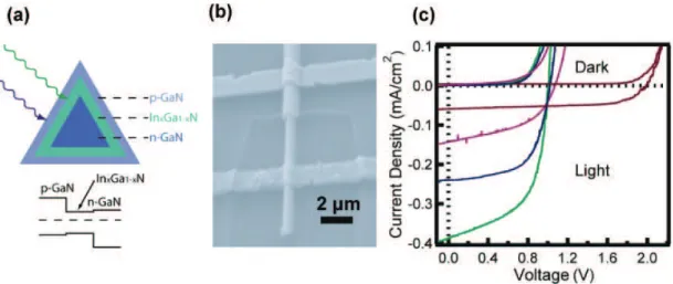
It has been proposed that the pyramidal-shaped sharp tip is caused by the low strain state in the interface of the homoepitaxy process [109]. If there exists biaxial strain in the interface, for example, the GaN structure grown on AlN or directly on c-sapphire, it will form truncated pyramidal shape or hexagonal pris-matic shape with a flat c-plane surface respectively even under the same growth conditions. This phenomenon is explained by the author taking into account the strain dependent Ehrlich-Schwoebel barriers across different planes. Later on, it has been further demonstrated that even on the homoepitaxial growth, the GaN structure can be turned from pyramid to hexagonal prism under a pulsed growth mode created by flow modulation [110] and this result was reproduced with strip patterned mask geometry to get flat c-plane and vertical a-plane shaped struc-ture for GaN epitaxy lateral overgrowth on micrometer sized circular opening [111]. The CL measurements on single pyramid object reveal a gradual 2-4 nm red-shift of NBE emission position from apices to base of the pyramid depending on the object diameter. This could evidence the Si and O impurity incorporation into the crystal lattice from the dielectric mask through surface diffusion with an estimation value of 108 cm−3 from finite element calculation [112].
It is worthwhile to note that, till now, the homoepitaxy SAG of hexagonal pyramidal shaped GaN structure in the nanoscale range with circular patterning mask geometry is not reported. More efforts are thus needed to study in detail the facet evolution for the growth of this nanoscale SAG GaN pyramids on GaN template.
2.2 MOVPE growth of III-nitride nanostructures
2.2.4
MOVPE III-nitride nanostructures based
heterostruc-tures growth for device applications
2.2.4.1 NW based heterostructures
The MOVPE synthesis of III-nitride NWs introduced in last part showed high crystalline quality compared to the 2D growth due to the effective relaxation of strain avoiding the creation of dislocations. These objects become excellent template to grow coaxial (mainly radial) heterostructures like In1−xGaxN/GaN or
Al1−xGaxN/GaN with successful doping and composition modulation with larger
lattice mismatches than in traditional planar structures. LED:
A core/multishell III-nitride nanoNW radial heterostructures has been used to fabricate the nano LED by Qian et al. from Prof. Charles Lieber’s group at Harvard University [43]. This Core/multishell nanoNWs were prepared by catalyst-assisted MOVPE giving a triangular shaped n-GaN core and In1−xGaxN
/GaN/p-Al1−xGaxN/p-GaN shells as shown in Figure 2.17 (a). Current versus
voltage characteristics (Figure 2.17 (b)) shows typical p-n diode current recti-fication with a sharp onset at around 3.5 V in forward bias. Normalized EL (Figure 2.17 (c) and (d)) of this nano LED exhibits distinct spectral peaks vary-ing from 367 to 577 nm with In compositions of about 1 to 35 % in the quantum well layer accomplished by reducing the growth temperature. In addition, devices exhibit dominant emission from the free NW ends (Figure 2.17 (e)).
Although this work has pioneered the fabrication of III-nitride LEDs based on NW geometry and shows the possibility to cover the green gap, this demonstration is based on single NWs, which basically do not meet the commercial product requirements.
Lee et al. in Prof. Gyu-Chul Yi’s group from National Seoul University fab-ricated ZnO/n-GaN/In1−xGaxN/p-GaN nanoarchitecture LED microarrays
con-sisting of position-controlled GaN/ZnO coaxial nanotube heterostructures as shown in Figure 2.18 (a) [52]. This technique uses ZnO nanotube arrays as template. Then a Si-doped n-GaN, three periods GaN/ In0.24Ga0.76N MQW were grown
to achieve the green emission from nanoarchitecture LED microarrays. Subse-quently, a Mg-doped p-GaN layer was deposited on top of the last GaN quantum barrier using a commercial nitride MOVPE system (Figure 2.18 (b)). The I-V curve exhibited typical rectifying behavior with a turn-on voltage of 3 V and a leakage current of 5×10⁴ A at -4 V. Above the turn on voltage, the current
in-2. PROPERTIES OF III-NITRIDE SEMICONDUCTORS AND THE NANOSTRUCTURES GROWN BY MOVPE
Figure 2.17: (a) Dark-field TEM image of a cross-sectional GaN/In1-xGaxN/GaN/AlGaN NW, (b) SEM image of the connected NW device with n and p metal pads and the corresponding I-V curve,(c) Normalized EL spectra of five representative NWs with different In content, (d) Optical microscopy images collected from around p-contact of NW LEDs in forward bias showing different col-ors, and (e) From left to right : optical microscopy image of NW LEDs with metal contact and the EL image recorded in a forward bias of 9 V and 11 V respectively.
crease very fast and at 100 mA most of the single nanoarchitecture emitting light at green range.
This kind of structure has made a great progress for the III-nitride NW based LED although the inconvenient lies in the switch between the two MOVPE reactors for ZnO and GaN growths. Such strategy using ZnO nanostructures was chosen due to the easy approach getting catalyst-free ZnO NWs by MOVPE.
Very recently, this group in collaboration with SAMSUNG demonstrated the synthesis of MOVPE SAG core-shell/axial III-nitride NWs for full visible spectrum tuneable LED [113]. This time GaN NWs are used instead of ZnO nanotubes as the core template to make a real homoepitaxy, but unfortunately the growth condition are not detailed. The basic strategy for epitaxial growth of multifaceted GaN nanostructures and fabrication of color-tunable LEDs is shown in Figure 2.19 (a). The GaN NW arrays were grown on n-GaN/c-sapphire sub-strates using SAG catalyst-free MOVPE. After the growth of GaN NW arrays, In1−xGaxN/GaN MQW layers were heteroepitaxially grown over the entire
sur-face of each GaN NW array (Figure 2.19 (b)). Subsequently, Mg-doped p-GaN was epitaxially coated on the NW with the MQW to form an overlayer film (inset
2.2 MOVPE growth of III-nitride nanostructures
Figure 2.18: (a) Schematic and (b) SEM images for GaN/In1-xGaxN/GaN/ZnO p-n homojunction coaxial nanoarchitecture heterostructure arrays, (c) Schematic for nanoarchitecture LED microarrays with ohmic metal contact and (d) Photogra-phy of light emissions from nanoarchitecture LED microarrays with 100 mA inject current.
of Figure 2.19 (b)). The HR-TEM analysis showed that the MQWs are formed on both the topmost and upright sidewall areas of the NW, respectively. A sig-nificantly difference in the QW and QB thicknesses and In composition in QW was observed (Figure 2.19 (c)). This anisotropically deposition of the MQW on the GaN NWs is believed to play a critical role in the color turnability of the NW embedded LEDs: a blue-shift of the EL spectrum position by increasing the forward voltage as shown in Figure 2.19 (d). Furthermore, by integrating three zones on single chip with different p-electrode area, a multicolor (red, blue, green) single inorganic LED chip was first time demonstrated with the same injection current of 20 mA (Figure 2.19 (e) and (f)).
Laser:
Optically pumped lasing operation of single GaN NWs with (In1−xGax
N/n-GaN)n (n= 3, 13, 26) MQW (thickness 1-3 nm) core-shell heterostructures at
room temperature has also been demonstrated by Qian et al. in Prof. Charles Lieber’s group from Harvard University [114]. The MQW NWs structure design
2. PROPERTIES OF III-NITRIDE SEMICONDUCTORS AND THE NANOSTRUCTURES GROWN BY MOVPE
Figure 2.19: (a) Fabrication process of GaN NW embedded LEDs, (b) tilted SEM and inset the cross-section TEM image of GaN NW array, (c) cross-section TEM image of GaN NW with In1−xGaxN MQW structure, (d) visible-color-turntable GaN NW LEDs under different forward bias and (f) visible-color-turntable GaN NW LEDs under same current flow with different p-contact area.
(Figure 2.20 (a)) consists of a triangular shaped GaN NW core, which behaviors as the primary part of the optical cavity, and epitaxial In1−xGaxN/GaN MQW
shells, which serve as the composition-tunable gain medium. Dark-field cross-section STEM revealed the MQW structure growths along the (1¯101) facets, but not along the third facet of the triangle, i.e. (000¯1) facet where the growth rate is very small (Figure 2.20 (b) and (c)).
The light emission recorded by optical microscopy from single NWs shows a wave guiding effect with enhanced luminescence intensity from the end part of the object as shown in Figure 2.20 (d). Figure 2.20 (e) is normalized photolu-minescence spectra acquired from four representative 26×MQW NW structures with increasing In concentration from 5-23 %. It evidences a lasing behavior with peak maxima at 383, 420, 452 and 478 nm, spanning a substantial portion of the ultraviolet to visible region of the electromagnetic spectrum. The threshold power densities for these four MQW NW lasers are all below 700 kW/cm2. It


![Figure 2.8: Schematic view of (a) the electrical polarization and sheet carrier layer in InGaN/GaN MQW heterostructures grown along [0001] direction and (b) the band diagram of this structure.](https://thumb-eu.123doks.com/thumbv2/123doknet/12882793.370128/29.892.174.665.216.504/figure-schematic-electrical-polarization-carrier-heterostructures-direction-structure.webp)
![Figure 2.10: Schematic view of (a) the electrical polarization and sheet carrier layer in InGaN/GaN MQW heterostructures grown along [1¯ 100] direction and of (b) the band diagram of this structure.](https://thumb-eu.123doks.com/thumbv2/123doknet/12882793.370128/30.892.238.727.216.465/figure-schematic-electrical-polarization-carrier-heterostructures-direction-structure.webp)