HAL Id: hal-02334401
https://hal.archives-ouvertes.fr/hal-02334401
Submitted on 26 Oct 2019
HAL is a multi-disciplinary open access
archive for the deposit and dissemination of
sci-entific research documents, whether they are
pub-lished or not. The documents may come from
teaching and research institutions in France or
abroad, or from public or private research centers.
L’archive ouverte pluridisciplinaire HAL, est
destinée au dépôt et à la diffusion de documents
scientifiques de niveau recherche, publiés ou non,
émanant des établissements d’enseignement et de
recherche français ou étrangers, des laboratoires
publics ou privés.
Circuit-type modelling of SiC power Mosfet in
short-circuit operation including selective fail-to-open
and fail-to-short modes competition
F. Richardeau, François Boige
To cite this version:
F. Richardeau, François Boige. Circuit-type modelling of SiC power Mosfet in short-circuit
opera-tion including selective fail-to-open and fail-to-short modes competiopera-tion. Microelectronics Reliability,
Elsevier, 2019, pp.113501. �10.1016/j.microrel.2019.113501�. �hal-02334401�
__________________________________________
* Corresponding author. frederic.richardeau@laplace.univ-tlse.fr
Circuit-Type modelling of SiC power Mosfet in short-circuit operation
including selective fail-to-open and fail-to-short modes competition
F. Richardeau
*, F. Boige
LAPLACE, University of Toulouse, CNRS, France
Abstract
SiC Mosfet has very unique properties in extreme operation such as a well-known fail-to-short failure mode but in competition with a lesser known fail-to-open failure mode. These two modes are generally studied and modelled separately, whereas, in practice, they are coupled with the junction temperature of the chip. This paper presents a circuit-type modelling approach of these two modes simultaneously. This modelling allows to simulate the selectivity and competition between these two modes, one is clearly critical and the other is advantageously safe. The proposed model is then compared with short-circuit test of 1.2kV-80m MOSFET SiC.
1. Introduction and objectives
SiC Mosfet converters have been spectacularly developed to combine both high efficiency and a high level of compactness. Applications in the fields of transport, railway and also grid-connected PV inverters are targeted in the range of 10kW to several 100kW, in a medium range voltage, from 400V to 900V [1]. The robustness of SiC Mosfet device and the management of its protection are also the subject of extensive research in many laboratories because its short-circuit time capability (TSC) is often lower than
Silicon devices and varies greatly from one manufacturer to another [2]. The very thin gate-oxide (typically 50nm against 100nm for silicone-planar device) under a high gate field (4MV/cm compared to 10MV/cm breakdown field of the SiO2) is highly
stressed in short-circuit operation. Indeed, the junction temperature can reach at least 1300K, leading to hot carrier injection in the oxide that could explain the possible weakness of the gate region and its variability in extreme operation [3], [4].
Thus SiC Mosfet has unique properties in short-circuit operation such as a competition between a well-known drain-source fail-to-short (FTS) failure mode (also named "hard" failure mode, or again "catastrophic" failure mode) and a lesser known drain-source fail-to-open (FTO) failure mode (also named "soft" failure mode) caused by a gate – source short-circuit path. The FTS mode, comes from a thermal runaway and/or the parasitic BJT latch-up leading to the semiconductor local destruction and the
creation of a metallic path drain-source [5]. The FTO mode, comes from the Al top metal fusion and diffusion, caused by the extreme heat in short-circuit, between the polysilicon gate and the Al source. The location of this metallic path can be either on top of the chip between the gate fingers and the source pad below the passivation layer, and/or across the ILD (Inter-Layer Dielectric) through metallized cracks [6]–[11] caused by a very low thermal expansion coefficient of the SiO2 compared to Al and SiC ones.
In this last case, gate and source electrodes are shorted leading to a FTO mode.
FTS and FTO modes are generally studied and modelled separately, whereas in practice they are coupled with the temperature of the chip. However, the thermal runaway of the FTS mode is governed by the local temperature at the maximum field along the depletion region, while the FTO mode is dependent of the top metal melting and the ILD cracks which are governed by the oxide thermo-mechanical capability. This paper presents for the first time a circuit-type modelling approach of the SiC Mosfet including the global thermal dynamic of the FTS and FTO modes simultaneously. This modelling allows to simulate the selectivity and competition between these two modes, one is clearly critical and the other is advantageously safe. The proposed model is then compared with short-circuit test of 1.2kV-80m MOSFET SiC. The paper is organized in four sections. Section 2 presents the circuit-type electro-thermal modelling of
a SiC Mosfet based on VGSth, IDsat and IGleak
thermal-dependency. Section 3, deals with the FTO and FTS modelling separately but using the same circuit-type approach which will be embedded in the same model base. Finally, in section 4, the two failure modes are put in competition situation along two short-circuit test and compared with experimentation. The first one under a reduced drain-source voltage, where a stable FTO mode occurs. The second one, under a nominal drain-source voltage where the FTS mode happens after an instable and incomplete FTO mode.
2. Circuit-type electro-thermal modelling
The short-circuit operation shows a very fast thermal dynamics over a wide temperature range (from 300K to more than 1500K in a dozen of µs). Such a stress dynamic can reveal specific drift mechanisms or even degradation mechanisms of weak region which are not visible in nominal operation [2]. For example, the strong gate-source leakage-current is caused by a hot electron injection through the thin gate oxide [4] and the high drain-source peak current decreases as the channel mobility decreases at high temperature [12]. As a matter of fact, in order to model and fit the thermal-dependant physical mechanisms involved during the short circuit operation, an extended electro-thermal modelling is needed. The authors previously presented in [13] a compact and non-segmented electro-thermal model including circuit elements as illustrated in Fig. 1. Note that in the following, all numerical values, unless otherwise specified, are fitted in relation with a 1.2kV-80m DUT, ROHM™ SCH2080 (generation II), based on an active area 12.4mm², in TO247 package.
2.1. First thermal modelling
Due to the very short transient operation (<100µs) clearly less than the thermal time constant of the chip,
a diffusive 1D thermal model is sufficient. Then an 1D Comsol™ model of the chip's layers has been developed [13] including the electric field distribution Ex around the P+/N- depletion region. This model is
fed by a time-dependant current density Jx(t) coming
from experimental curves. At this stage, the gate regions, with polysilicon gate fingers, SiO2 and the
ILD are not modelled because of their very small thickness (<1µm) and the possible mesh size problem in a FEM approach. A single temperature value is therefore considered in the thermal modelling, named
Tj in the depletion zone at the maximum electric field
position. However, the thickness of the top Al metal layer is only taken into account with an increase of the P-well thickness. Note that in SiC structure, the drift region is realized by a very fine epitaxy layer of about ten microns compared to a 300µm substrate. The gate oxide is also very thin (50nm) on which the Al layer is only 5µm thick. Given the small dimensions involved in the active zone, we have shown in [13] that the thermal gradient between the maximum electric field position and the gate region is very limited. Then authors only consider the temperature at the maximum electric field position of the depletion zone. In order to adapt this model into PLECS™, the 1D model can be either discretized at a constant geometric step x or fitted on a time-domain response to extract an equivalent Cauer's line (Rthi, Cthi) with a
reduced number of cells (typically 30) or embedded by means of a vectorization formalism in a PLECS' functional block. Moreover, due to the "snap" effect of the electric field peak localized around the depletion region, a distributed power heat flux along the 1D x-axis is not necessary. Then a localized input instantaneous heat flux [W, t] connected at the input port of the Cauer's line is sufficient.
2.2. Electric modelling
It has been shown in [2] that the gate leakage-current can be modelled by an ohmic gate-source dipole whose value is in relation to the temperature inside the gate region. Relation (1) gives the behavioral gate leakage-current model in relation to the adiabatic thermal energy accumulated during the short-circuit sequence (En) by means of a polynomial equivalent
conductance. It is specifically fitted using the fit Matlab™ optimization function with experimental values. An offset function is also introduced which is independent of the gate polarization. In this relation, pij coefficients are in relation to the drain-source
voltage applied to the DUT. For 600V, Tcase = 25°C
and VGS [18V, 21.5V], it was extracted : p01 = 9.51,
p11 = 9.44, p21 = 2.512, p00 = -156.08, p10 = -150.35,
p20 = -36.05, p30 = 0.628.
Fig. 1. Electro-thermal PLECS™ Circuit-type modelling-base for SiC Mosfet in short-circuit operation. FIGleak, FVGSth, FIDsat are respectively
IGleak = (p01+ p11𝐸𝑛+ p21𝐸𝑛2). VGS+
p00+ p10𝐸𝑛+ p20𝐸𝑛2+ p30𝐸𝑛3 (1)
Relations (2) is the well-known physical relations modelling the saturation current (IDsat). Relation (3)
model the channel mobility (µn) in function of the
temperature (Tj) using the Matheissen's mobility rule
[14]. Relation (4) model the threshold voltage (VGS(th))
as an equivalent linear model [15].
IDsat 𝑇𝑗 = μn 𝑇𝑗 ∙ Cox∙ Z 2L . 𝑉𝑔𝑠− Vgs th 𝑇𝑗 2 2 μn 𝑇𝑗 = μa0 𝑇𝑗 T0 a 1 +μa0 μb0 𝑇𝑗 T0 b−a +μa0 μc0 𝑇𝑗 T0 c−a (3) VGS th 𝑇𝑗 = x1∙ 𝑇𝑗+ x2 4
Where: µa0, μb0, μc0 are mobility parameters at
ambient temperature (300K) and a, b and c are sensitive thermal coefficients which have been fitted with experimental measures and temperature extracted from the thermal model presented in the previous subsection in order to obtain a wide range temperature model: [in cm².V-1.s-1], µ
a0 = 2.33, μb0 =
2.95, µc0 = 1.94.103 and: a = -1.48, b = -4.8, c = 2.56.
In the same conditions thee threshold voltage parameters, x1 and x2, have been extracted: x1 = -0.025
V/K, x2 = 15.4V.
2.3. First validation of the electro-thermal model
The previous model is evaluated in a short-circuit
simulation with a 12µs pulse for two values of VGS = 18V and 21V, results are presented in Fig.2. In
both cases, the model accurately represents the gate leakage-current with only a few % error. The drain-source current is slightly over-estimated for VGS = 21V while it is slightly under-estimated for
VGS = 18V. However, the estimation of the adiabatic
energy remains very accurate. Note this one greatly exceeds 1000K after 10µs. Such a temperature level is in agreement with recent publications using the same modelling approach but on different chips' size [16] or considering a different VDS bias [17].
3. Fail-to-open and Fail-to-short modelling
In this section the previous electro-thermal model is extended to include FTO and FTS modes. These will be modelled separately because they represent different mechanisms which will be explained in this section.
3.1. FTO mode analysis and modelling
Previous thermal simulations shown that the maximum junction temperature near to the top surface can significantly exceed the melting temperature of the Al layer (660°C or 933K) [13]. Some failure analysis have shown that the Al fusion cause metallic bridges between source and gate electrodes only if the heat power density is limited by mean of a reduced drain-source voltage Vsupply 450V instead of 600V
[18], [19].
As shown in Fig. 3, below a given drain-source voltage, the FTO mode is guaranteed. Above this
Fig. 2. Type 1 short-circuit SiC MOSFET model evaluation in PLECS™ software for different buffer voltages bias (@VDS = 600V, Tjinit = 25°C and RG = 47Ω).
Fig. 3. Experimental FTO and FTS modes in type 1 short-circuit operation for VDS = 600V (cascaded
modes) in blue curve and for VDS = 400V in black
curve, (@Tjnit = 25°C, Vbuffer(on/off) = 18V/-5V and
RG=47Ω). VG S (V ) IG (m A ) IDS (A ) VD S (V ) IDS VDS VDS=600V VDS=400V t (µs) t (µs) t (µs) 1st FTO 2nd FTS 1st FTO 1st FTO 2nd FTS 2nd FTS FTO FTO FTO
voltage the FTO mode is overtaken by the FTS mode which will be described in §3.2. Indeed, for a reduced drain-source voltage, the heat power density is limited, which therefore reduces the junction thermal dynamics of the chip, allowing a sufficient delay time for the top Al metal to diffuse under the passivation of the chip to form a stable Al metal bridge leading to the device natural turn-off and cooling [19]. In addition, thermal shocks at the Al-SiO2/ILD and Al-SiC
interfaces yield significant differential strains which causes cracks and metal infiltration between source electrode and gate fingers as it was seen on others SiC devices [7]–[10]. These two metallurgical and thermo-mechanical mechanisms allow to understand the origin of the FTO mode [6], [18], [19].
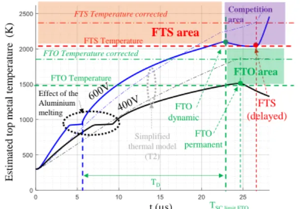
In Fig. 4, the top metal temperature estimation from the experimentation is presented the colours of Fig.3 are respected. The temperature is estimated with an enhanced version of the 1D thermal model presented in §2.2. The thermal sensitivity of the thermal conductivity and the specific heatcapacity of the chip materials (Al and SiC) are also modelled from [20], [21] as well as the Al phase-transition from solid to liquid state around 660°C (933K). Based on [20], the heat capacitance in the solid state and the liquid state is displayed in Fig. 5. Relation (5) gives respectively the relation between the solid state capacitance to the fusion state model to the liquid state model.
Cp= CpS T ∙ 1 − α T + CpL∙ α T + Lf∙ dα dT (5)
With : CpS, solid state heat capacitance which is
temperature-dependent [20]; Lf, heat of fusion
(Lf = 397 kJ/kg [20]); CpL, liquid state heat
capacitance which is typically considered as a
constant value (Cpl = 1.175kJ/(kg.K) [20]); 𝛼 𝑇 is a
phase transition function chosen as a cumulative function of a normal distribution (6) as also illustrated in Fig. 5. The normal distribution is centered in Tf and
with a variance 𝜎 = 5𝐾. The solid and liquid phases of the heat capacitances are combined with the phase transition function to have a smooth transition during fusion. The integration of the normal law gives 1 and multiplying it by the heat of fusion gives the amount of latent heat released during the phase transition. The transition will take place on the interval 6𝜎 = Δ𝑇𝑠→𝑙.
For aluminum and also to ensure the convergence of the numerical model, Δ𝑇𝑠→𝑙 = 30𝐾. During that
time, the material is supposed in a mixed state between solid and liquid.
𝛼 𝑇 = ∫−∞𝑇 𝑑𝛼𝑑𝑇 𝑥 𝑑𝑥 (6)
The proposed modelling is by default implemented in Comsol™. The solid line curves in Fig. 4 show that it allows to simulate by a quasi-plateau corresponding to the quantity of latent energy to be dissipated in order to produce the Al layer phase change. [16] recently proposed the same modelling approach based on our work by including a sensitivity study to the physical parameters.
Concerning the circuit-based electro-thermal modelling of the DUT, these curves are fitted by a Cauer's line of 8 elements with constant parameters to easily allow an integration in PLECS™. The responses of the Cauer's lines are superimposed in a dotted line in Fig. 4. This line represents the simulated response in a very average way and therefore above all in a qualitative way.
The conditions to access the FTO area safely is presented by means of a "green safe area" in the transient thermal domain: the junction temperature must be at least 1500K and at least 17µs after the total melting of the Al, called delay time (TD). The
reference [6] showed that the quasi same FTO temperature is obtained for a different chip manufacturer but with a smaller size and therefore
Fig. 5. Thermal-dynamic heat capacitance modelling of Al layer for FTO modelling.
Temperature (K) Tf CpSolid CpLiquid T h er m al c ap ac it y (J /( k g .K )) Tf T h er m al c ap ac ity (J /(k g .K )) Cptotal Lf α T Cptotal Lf α T CpLiquid CpSolid Temperature (K) Zoom ∆Ts→l=6σ Sol id P has e Liqui d P ha se Solid Phase Liquid Phase
Fig. 4. Simulated temperature from waveforms presented in Fig. 3. The simulation includes melting Al (transition phase) and experimental comparison (dots). FTO, FTS modes and competition areas definition. Black curve VDS =400V, blue curves VDS = 600V
@Tjinit = 25°C, Vbuffer = 18V. t (µs) E st im at ed top m et al tem p eratu re (K ) FTO dynamic FTO Temperature TSC limit FTO FTS (delayed) Effect of the Aluminium melting Simplified thermal model (T2) FTS Temperature FTS Temperature corrected TD
FTO Temperature corrected
FTS area FTO permanent Competition area FTO area
with a lower Tsc. Only 100K separates the two FTO temperatures of the two chips while the sizes are in a 1.2 ratio and the Tsc in a 2 ratio. These results show that the FTO thermal level is not very variable over a wide range of chip characteristics.
Given the significant temperature difference involved, we believe that the two failure mechanisms are well differentiated. Moreover, experimentally, the authors have verified the existence of these two types of failure-modes on a set of about ten DUTs components. The dispersion is not significant either on the TSC value (17µs) or on the specific drain –
source voltage value, VDS 400V, that define the
boundary between the two modes.
3.2. FTS mode analysis and modelling
As seen in Fig. 3 with the blue curve (VDS = 600V),
the FTS mode is triggered before the consolidation of a complete FTO mode. Such a model concerns the representation of the drain-source leakage current by thermal generation [5]. A Shockley-Read-Hall (SRH) carriers generation model is used by means of relation (8) [5], [22] because it allowed to represent globally the drain leakage obtained in an experimental way. The thermal runaway dynamic of this leakage leads to the FTS mode. In SRH generation , WD is the space of
charges width in short-mode under VDS defined in
relation (9) and ni the intrinsic density of charge
carriers described in relation (10) [23].
𝐼𝑡ℎ 𝑇 =𝑞𝑊𝐷𝜏𝑛𝑖 𝑇 𝑔 S (8) 𝑊𝐷= √2𝜖𝑞𝑠∙𝑁𝑁𝑑+𝑁𝑎 𝑑𝑁𝑎 ∙ 𝑉𝐷𝑆 (9) 𝑛𝑖𝑆𝑖𝐶 𝑇 = 1.7 ∙ 1016∙ 𝑇 3 2∙ 𝑒− 2.08∙104 𝑇 (10)
With: g, is the SRH generation lifetime [1ns, 1s]
from [21][24]. We used this parameter g as a fitting
variable (fixed at 1ns) so that our model produces the same drain –source current and failure time at 600V than the experiment. This fit was also evaluated at 400V giving a Tsc value in FTO mode very close to
the experiment. Our model is therefore robust. The results of this model is presented in the next section in the simulation vs experimentation.
4. FTO and FTS modes competition: simulation vs experimentation
The complete proposed model is depicted in Fig. 6. In addition to electro-thermal modelling of the gate leakage-current, drain-source current and threshold voltage as described in §2, a dedicated FTO and FTS circuit-parts have been included. FTO mode is
modelled by a gate-source parallel failed-resistor Rgdef
(0.1) controlled by switch S3 and associated with
switch S2 to force the channel turn-off. These two
switches are managed by the functional block diagram presented in Fig. 7: if the top metal estimated temperature is higher than the Al fusion temperature (933K) and the FTO threshold temperature TFTO after
the delay time Td (17µs), the FTO mode is triggered
by a latch gate. As illustrated in Fig. 4, the estimated temperature comes from a simplified fitted Cauer's line on the phase-transition curve of the top metal temperature. This thermal line is named Ttop in Fig.6.
FTS mode is modelled by a parallel leakage drain-source controlled current-drain-source Ith and FIth block that
includes the SRH generation model studied in §3.2. This block is fed by the same thermal line Ttop. If the
estimated temperature is higher than TFTS, the FTS
mode is triggered and a dedicated switch S1 force the
turn-on through a failed resistor Rdef (5m).
The evaluation of the model is given in Fig. 8 in comparison with experimental results from a test-bench described in [2]. At nominal voltage, in Fig. 8a), due to the high thermal dynamic stress applied to the chip, the proposed model is able to highlight the
Fig 6. Final proposed electro-thermal SiC Mosfet model for short-circuit simulation including FTO and FTS modes modelling.
Fig 7. FTO and FTS functional blocks management for the model configuration described in Fig. 7, with : Tftscorrected = 2400K , TfusAl = 933K, Tfto corrected = 1900K.
cascaded FTO and FTS modes: the drain-source leakage current is too high to prevent thermal runaway. Note that the dedicated drain-source leakage component is drawn in dashed line. At reduced voltage but with the same pulse duration, in Fig 8b), due to the low thermal dynamic stress applied to the chip, the FTO mode is the unique and stable mode. The low drain-source leakage current is clearly not enough to trigger the thermal runaway and the FTS mode does not appear.
5. Conclusion
In this article, the authors proposed a complete electrothermal circuit-type model for SiC Mosfet in short-circuit operation able to reproduce the new FTO mode in conjunction with the well-known FTS failure
modes. The modelling of the dynamic drain-source carriers thermal generation combined with the FTO and FTS thermal thresholds allow to predictively simulate and to highlight either a specific cascaded failure modes at nominal voltage or an original safe FTO mode at low voltage as analysed from experimentation. This approach complements and extends in an original way the known electrothermal power device models. Finally, the proposed compact model has the following uses and interest:
- modelling and prediction of the TSC and ESC
(robustness study model),
- modelling and prediction of failure-modes (failure modes study model),
- modelling separately IGS (leakage), VGS drop and
IDSS (leakage) (diagnostic study model).
- fully compatible with gate driver protection design or fault propagation analysis in different conversion architectures.
Acknowledgements
This research work received financial support from the French National Research Agency (ANR). Project name: HIT-TEMS managed by CNAM Paris and Satie lab.
References
[1] Z. Lim, Y. Liu, L. Zhang, J. Pou, R. Simanjorang, and A. Gupta, ‘Design of 100 kVA SiC Power Converter for Aircraft Electric Starter Generator’, in
2018 IEEE 4th Southern Power Electronics Conference (SPEC), 2018, pp. 1–9 https://doi.org/10.1109/SPEC.2018.8635866. [2] F. Boige and F. Richardeau, ‘Gate leakage-current
analysis and modelling of planar and trench power SiC MOSFET devices in extreme short-circuit operation’, Microelectron. Reliab., vol. 76–77, no. Supplement C, pp. 532–538, Sep. 2017 https://doi.org/10.1016/j.microrel.2017.06.084. [3] F.-C. Chiu, ‘A Review on Conduction Mechanisms
in Dielectric Films’, Advances in Materials Science
and Engineering, 2014. [Online]. Available:
https://www.hindawi.com/journals/amse/2014/5781
68/. [Accessed: 20-Dec-2017]
https://doi.org/10.1155/2014/578168.
[4] F. Boige, D. Trémouilles, and F. Richardeau, ‘Physical origin of the gate current surge during short-circuit operation of SiC MOSFET’, IEEE
Electron Device Lett., pp. 1–1, 2019 https://doi.org/10.1109/LED.2019.2896939. [5] Z. Khatir, S. Lefebvre, and F. Saint-Eve,
‘Experimental and numerical investigations on delayed short-circuit failure mode of single chip IGBT devices’, Microelectron. Reliab., vol. 47, no.
2, pp. 422–428, Feb. 2007
https://doi.org/10.1016/j.microrel.2006.05.004. [6] F. Boige, F. Richardeau, S. Lefebvre, J.-M.
(a) VDS=600V
(b) VDS=400V
Fig 8. Comparison between the proposed model and the short-circuit failure modes experimentation at Vbuffer =
18V : a) cascaded FTO and FTS modes for VDS = 600V,
b) unique and stable FTO mode for VDS = 400V.
VG S (V ) IG (m A ) IDS (A ) VD S (V ) IDS VDS Measure Simulation t (µs) Ith IDS IDsat FTS Thermal runaway FTO Measure Simulation IDS VDS FTO Ith IDS IDsat VG S (V ) IG (m A ) IDS (A ) VD S (V ) t (µs)
Blaquière, G. Guibaud, and A. Bourennane, ‘Ensure an original and safe “fail-to-open” mode in planar and trench power SiC MOSFET devices in extreme short-circuit operation’, Microelectron. Reliab., vol. 88–90, pp. 598–603, Sep. 2018 https://doi.org/10.1016/j.microrel.2018.07.026. [7] F. Boige, F. Richardeau, D. Trémouilles, S.
Lefebvre, and G. Guibaud, ‘Investigation on damaged planar-oxide of 1200V SiC power MOSFETs in non-destructive short-circuit operation’, Microelectron. Reliab., vol. 76–77, no. Supplement C, pp. 500–506, Sep. 2017 https://doi.org/10.1016/j.microrel.2017.06.085. [8] R. Ouaida, M. Berthou, J. León, X. Perpiñà, S. Oge,
P. Brosselard, and C. Joubert, ‘Gate Oxide Degradation of SiC MOSFET in Switching Conditions’, IEEE Electron Device Lett., vol. 35, no. 12, pp. 1284–1286, Dec. 2014 https://doi.org/10.1109/LED.2014.2361674. [9] P. D. Reigosa, F. Iannuzzo, and L. Ceccarelli, ‘Effect
of short-circuit stress on the degradation of the SiO2 dielectric in SiC power MOSFETs’, Microelectron.
Reliab., vol. 88–90, pp. 577–583, Sep. 2018
https://doi.org/10.1016/j.microrel.2018.07.144. [10] J. Wang, X. Jiang, Z. Li, and J. S. GAE,
‘Short-Circuit Ruggedness and Failure Mechanisms of Si/SiC Hybrid Switch’, IEEE Trans. Power
Electron., pp. 1–1, 2018
https://doi.org/10.1109/TPEL.2018.2839625. [11] S. Mbarek, P. Dherbécourt, O. Latry, and F. Fouquet,
‘Short-circuit robustness test and in depth microstructural analysis study of SiC MOSFET’,
Microelectron. Reliab., vol. 76–77, pp. 527–531,
Sep. 2017
https://doi.org/10.1016/j.microrel.2017.07.002. [12] T. T. Mnatsakanov, L. I. Pomortseva, and S. N.
Yurkov, ‘Semiempirical model of carrier mobility in silicon carbide for analyzing its dependence on temperature and doping level’, Semiconductors, vol. 35, no. 4, pp. 394–397, Apr. 2001 https://doi.org/10.1134/1.1365181.
[13] F. Boige, F. Richardeau, S. Lefebvre, and M. Cousineau, ‘SiC power MOSFET in short-circuit operation: Electro-thermal macro-modelling combining physical and numerical approaches with circuit-type implementation’, Math. Comput. Simul.,
Sep. 2018
https://doi.org/10.1016/j.matcom.2018.09.020. [14] S. Potbhare, N. Goldsman, A. Lelis, J. M. McGarrity,
F. B. McLean, and D. Habersat, ‘A Physical Model of High Temperature 4H-SiC MOSFETs’, IEEE
Trans. Electron Devices, vol. 55, no. 8, pp. 2029–
2040, Aug. 2008
https://doi.org/10.1109/TED.2008.926665. [15] B. J. Baliga, Modern power devices. Wiley, 1987. [16] Y. Pascal, M. Petit, D. Labrousse, and F. Costa,
‘Thermal simulations of SiC MOSFETs under short-circuit conditions influence of various simulation parameters’, presented at the International Workshop on intergradted power packaging, 2019.
[17] A. Tsibizov, I. Kovacevic-Badstuebner, B. Kakarla, and U. Grossner, ‘Accurate Temperature Estimation
of SiC Power MOSFETs under Extreme Operating Conditions’, IEEE Trans. Power Electron., pp. 1–1, 2019 https://doi.org/10.1109/TPEL.2019.2917221. [18] D. Othman, Etude d’interrupteurs en carbure de
silicium et potentiel d’utilisation dans des applications aéronautiques. Paris Saclay, 2015.
[19] G. Romano, A. Fayyaz, M. Riccio, L. Maresca, G. Breglio, A. Castellazzi, and A. Irace, ‘A Comprehensive Study of Short-Circuit Ruggedness of Silicon Carbide Power MOSFETs’, IEEE J.
Emerg. Sel. Top. Power Electron., vol. 4, no. 3, pp.
978–987, Sep. 2016
https://doi.org/10.1109/JESTPE.2016.2563220. [20] J. E. Hatch, Aluminum: Properties and Physical
Metallurgy. ASM International, 1984.
[21] L. L. Snead, T. Nozawa, Y. Katoh, T.-S. Byun, S. Kondo, and D. A. Petti, ‘Handbook of SiC properties for fuel performance modeling’, J. Nucl. Mater., vol. 371, no. 1, pp. 329–377, Sep. 2007 https://doi.org/10.1016/j.jnucmat.2007.05.016. [22] Z. Wang, X. Shi, L. M. Tolbert, F. Wang, Z. Liang,
D. Costinett, and B. J. Blalock, ‘Temperature-Dependent Short-Circuit Capability of Silicon Carbide Power MOSFETs’, IEEE Trans. Power
Electron., vol. 31, no. 2, pp. 1555–1566, Feb. 2016
https://doi.org/10.1109/TPEL.2015.2416358. [23] B. J. Baliga, Silicon Carbide Power Devices. World
Scientific, 2005.
[24] N. G. Wright, D. J. Morrison, C. M. Johnson, and A. G. O’Neill, ‘Electrothermal Simulation of 4H-SiC Power Devices’, Materials Science Forum, 1998.
[Online]. Available:
https://www.scientific.net/MSF.264-268.917.
[Accessed: 27-Jun-2019]
https://doi.org/10.4028/www.scientific.net/MSF.26 4-268.917.