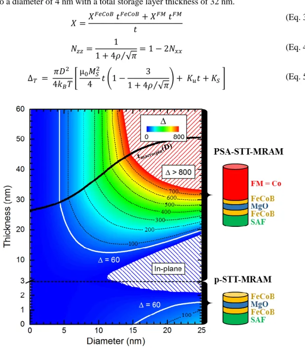
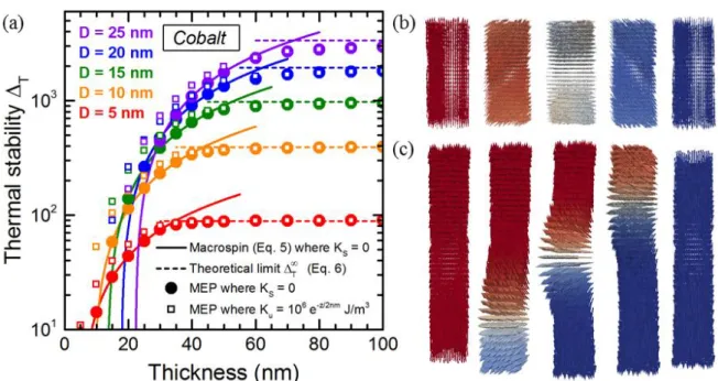
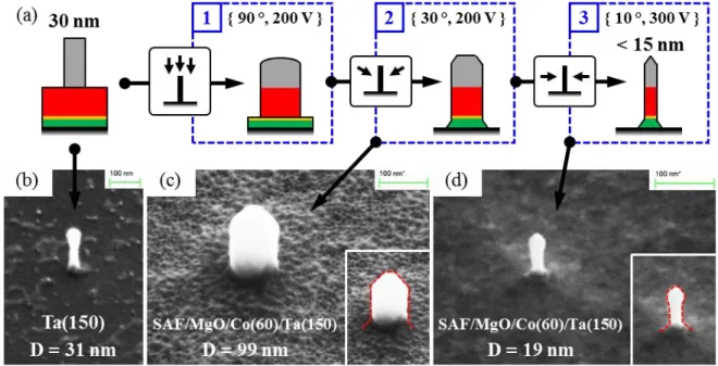
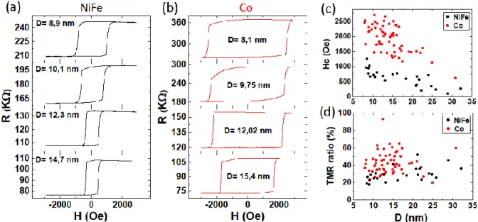
A highly thermally stable sub-20 nm magnetic random-access memory based on perpendicular shape anisotropy
Texte intégral
Figure


Documents relatifs
First, the case study is concerned with urban policy mobilities in security and surveillance matters – namely, the transnational circulation and reproduction of best practices in
Consequently, in order to compare our results in LiCl-LiF with pure fluoride salt, instead of listing ap- parent redox potentials, the difference between reduction peak po- tentials
Using these displacement vectors, an initial segmentation is performed on the first pair of frames, clustering vertices into static, stretched and rigidly moving regions..
(A) Fluorescence photomicrographs of vertical sections through mouse retina double immunolabeled for dystrophins, ε-SG, β-SG, δ-SG, γ-SG and SSPN in red and a cell marker of
[3] Georges Bastin and Jean-Michel Coron, Stability and boundary stabilization of 1-D hyperbolic systems, Progress in Nonlinear Differential Equations and their Applications, vol..
(Note: LBD calculated for a subgraph will still find the maximum degree node, hence the maximal degree nodes may appear in more than one subgraph.) Thus we have one
Obtain reference for read alignment: Download a Nematostella vectensis genome or transcriptome assembly from one of the sources in Table 1.. Trim reads (optional): While read
3 نكلو ،ثحابلا اهسردي يتلا ةلكشملل لمتحم لح وأ ريسفت نع ةرابع يه ةيملعلا ةيضرفلا ربتعت يتلا تانايبلاو قئاقحلا عمجل ةبسانملا
