HAL Id: hal-01917904
https://hal.archives-ouvertes.fr/hal-01917904
Submitted on 4 Feb 2019
HAL is a multi-disciplinary open access
archive for the deposit and dissemination of
sci-entific research documents, whether they are
pub-lished or not. The documents may come from
teaching and research institutions in France or
abroad, or from public or private research centers.
L’archive ouverte pluridisciplinaire HAL, est
destinée au dépôt et à la diffusion de documents
scientifiques de niveau recherche, publiés ou non,
émanant des établissements d’enseignement et de
recherche français ou étrangers, des laboratoires
publics ou privés.
Crack-Free Silicon-Nitride-on-Insulator Nonlinear
Circuits for Continuum Generation in the C -Band
Houssein El Dirani, Marco Casale, Sebastien Kerdiles, Carole Socquet-Clerc,
Xavier Letartre, Christelle Monat, Corrado Sciancalepore
To cite this version:
Houssein El Dirani, Marco Casale, Sebastien Kerdiles, Carole Socquet-Clerc, Xavier Letartre, et al..
Crack-Free Silicon-Nitride-on-Insulator Nonlinear Circuits for Continuum Generation in the C -Band.
IEEE Photonics Technology Letters, Institute of Electrical and Electronics Engineers, 2018, 30 (4),
pp.355-358. �10.1109/LPT.2018.2790045�. �hal-01917904�
Abstract—We report on the fabrication and testing of
silicon-nitride-on-insulator (SiNOI) nonlinear photonic circuits for complementary metal oxide semiconductor compatible monolithic co-integration with silicon-based optoelectronics. In particular, a process has been developed to fabricate low-loss crack–free Si3N4
730-nm-thick films for Kerr-based nonlinear functions featuring full process compatibility with existing silicon photonics and front-end Si optoelectronics. Experimental evidence shows that 2.1-cm-long nanowires based on such crack-free silicon nitride films are capable of generating a frequency continuum spanning 1515-1575 nm via self-phase modulation. This work paves the way to time-stable power-efficient Kerr-based broadband sources featuring full process compatibility with Si photonic integrated circuits (Si-PICs) on CMOS-lines.
Index Terms—Complementary metal-oxide-semiconductor
(CMOS), photonic integrated circuits (PICs), frequency continuum, nonlinear optics, silicon-nitride-on-insulator (SiNOI).
I. INTRODUCTION
ILICON-based photonic integrated circuits (Si-PICs) provide a key technology platform paving the way toward a brand-new optoelectronics featuring a considerable integration potential with cost-effective complementary metal-oxide-semiconductor (CMOS) technology and micro-nano-electronics circuits and nodes [1], [2]. Moreover, the high-index contrast of silicon-on-insulator (SOI) materials allows for the implementation - over small footprints - of optical functions providing us with the whole silicon photonics toolbox such as optical resonators and laser integration [3], input/output (I/O) couplers [4], high-speed modulators [5], Si-Ge photodiodes [6], as well as filters and wavelength (de)multiplexers [7]. However, the effort in hetero-integrating III-V lasers on silicon for generating on-chip multiple-wavelength optical signals for both Si-based telecom and integrated spectroscopy applications might soon reach a footprint bottleneck. More specifically, most of the research and development effort was spent in recent years on distributed Bragg reflector (DBR)- [3] and distributed feedback (DFB)-based architectures[10] capable of providing on-chip light emission to be fed into ring or Mach-Zehnder-based modulators [11] in order to accomplish data transmission with non-return-to-zero or more complex modulation formats for higher aggregate bandwidth. The main drawback sticking with such solutions is coming from the global bandwidth limit that can be achieved by using a single-wavelength emitting source as well as from their contribution to the power consumption of the optical link in term of pJ per transmitted bit
Manuscript received October 13, 2017, revised November, 10, December 24. H. El Dirani, M. Casale, S.Kerdiles, C.Socquet-Clerc and C. Sciancalepore are with the Commissariat à l’énergie atomique et aux énergies alternatives, CEA-LETI, Minatec, Département Optronique,F-38054 Grenoble, France (e-mail: houssein.eldirani@cea.fr).
C. Monat and X. Letartre are with the Ecole Centrale de Lyon, Institut des Nanotechnologies de Lyon (INL), UMR CNRS 5270, F-69130, Ecully, France. Digital Object Identifier XX.XXXX/LPT.2017XXXXXXX
Copyright (c) 2017 IEEE
(pJ/bit). For example, in the case of an III-V-on-Si DFB laser, more than 350 mW of electrical DC and radio-frequency powers are in fact necessary to feed light to modulators, which can run up to 50-60 Gb/s due to their intrinsic electro-optical bandwidth limitations. A possible solution to this drawback is to use reconfigurable (or tunable) lasers in order to exploit multiple-wavelength transmitting channels, counting a different wavelength for each subcarrier. This solution requires wavelength tuning, using e.g., heaters, which increase both the circuit complexity and power consumption. Another way to increase link capacity, while keeping steady the energy-per-bit is to shrink the size of the laser diodes by using micro-disk architectures [8] or vertical-cavity surface-emitting lasers on Si [9], having access to a larger number of wavelengths. Moreover, recent solutions based on comb laser-driven dense wavelength-division multiplexing (DWDM) silicon photonic transmitters via microring modulators may well increase the total aggregate bandwidth of the link, but the number of transmission channels remains limited to the quantum dot gain region, typically a few nanometers [12]. A paradigm shift in optical transmission and integrated spectroscopy can be brought forward by exploiting the full potential of 3) nonlinear optical
processes to generate optical frequency continua. Hundreds of optical frequencies can be obtained in III-V alloys nanowires with remarkable time-scale system stability [13] and in optical parametric oscillators (OPOs) [14]-[16], thus substituting an equal amount of III-V-on-Si individual laser diodes to be integrated on a chip, as illustrated in Fig. 1. Nevertheless, III-V materials need to be heterointegrated on silicon chips, making this solution more costly and complicated to realize. Concerning CMOS-compatible materials, prior work based on stoichiometric Si3N4-based nonlinear nanowires and OPOs
made use of high-temperature annealing (~1200 °C) of the nitride film and silica upper-cladding to break N-H bonds otherwise causing absorption in the C-band [14]. Besides, substrate preparation made by etching crack-limiting trenches in the SiO2 bottom-cladding or damascene process has been
used to prevent the propagation of tensile strain-related cracks in the nitride film [15], [16]. Although it resulted in relatively good performance, this approach may eventually hinder the straightforward integration of such nonlinear circuits on existing Si-based photonics and optoelectronics. First, extreme annealing temperatures are likely to degrade the silicon optical layer underneath along with its optoelectronic functionalities (e.g., modulation and photodetection). Secondly, beyond cracks formation in the silicon nitride films, high stress would result in significant wafer bowing (~ 500 µm) and consequent difficult automated handling, thus preventing the access over several pieces of equipment of a typical CMOS line. We report here on the development of a new CMOS-compatible crack-free process for the deposition of nitride-based films on 200- and 300-mm wafers for Si-PICs.
Houssein El Dirani,Marco Casale, Sébastien Kerdiles, Carole Socquet-Clerc, Xavier Letartre, Christelle Monat, and Corrado Sciancalepore
Crack-Free Silicon-Nitride-on-Insulator Nonlinear
Circuits for Continuum Generation in the C-Band
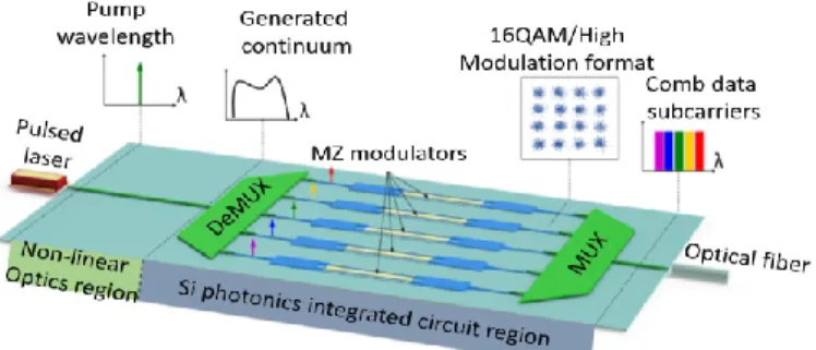
Figure 1 - Principle of ultra-high-speed-rate communications using nonlinear integrated optics. Artistic view of a future ultra-high-rate transmitter, integrating a frequency continuum broadband source onto a silicon optoelectronic chip.
This approach overcomes the aforementioned drawbacks of the SiN material platform, while remaining suitable for nonlinear applications. Section II presents the whole fabrication process of the silicon nitride waveguides. Section III is mainly devoted to the passive optical measurement, while section IV presents and discusses the nonlinear response of our silicon nitride waveguides. Section V concludes the work and provides readers with perspectives over future developments.
II. SILICON NITRIDE TECHNOLOGY
The whole process was based on 200-mm silicon wafers and developed on LETI CMOS pilot lines.
Deposition method. The fabrication starts with the 3-µm-thick
thermal oxidation of the silicon substrate. In order to control strain and to prevent cracks from appearing, the silicon nitride layer is deposited via low pressure chemical vapor deposition (LPCVD) in two (or more) steps counting a 365-nm-thick layer each. Between the subsequent deposition stages, the carrier wafer is rotated by 45° in order to distribute the uniaxial strain along the overall film thickness. As indicated in the introduction, the uniaxial stress would be accumulated in the case of the rotation-less wafers resulting in a significant bowing hindering the access to other tools of the CMOS line and creating cracks in the nitride film. Each deposition run is carried out at 780 °C with post-deposition cooling to around 630 °C for 20 minutes then ramp-up to 780 °C at 10 °C/minute in order to accomplish the second deposition. This process ensures against tensile-strain-related cracks, while providing a relatively thick nitride film exhibiting good optical properties across the full wafer. The deposition is carried out in a vertical chamber under a 112 mTorr pressure using NH3 and dichlorosilane (SiH2Cl2)
as precursor gases, respectively introduced in the chamber at 200 sccm and 80 sccm flow rates. By measuring the wafer bow, before and after removing the silicon nitride from the wafer back side, the material morphological characterization - using Stoney formula - revealed a tensile strain around +1200 MPa. The high tensile strain is a clear indication of the stoichiometry of the material.
Lithography and dry etching technique. Deep-UV (DUV)
lithography was performed on a ASML-300 stepper using 248-nm DUV and 780-248-nm-thick M78Y resist mask followed by a 40-nm-thick bottom anti-reflection coating (BARC). Fluoride-based dry etching was used to pattern the different architectures on the Si3N4 film previously deposited using solely the resist as
hard mask and the SiO2 buried oxide as an
Figure 2 – (a) Scanning electron microscope and (b) focused ion beam images of Si3N4-based nanowires before encapsulation.
etch-stop layer. In detail, a CF4-CH2F2-O2 chemistry was used
in a 300-mm reactor under 32 mTorr pressure and 150°C process temperature. A 20-second SiO2 overetch was estimated
to range between 20 nm and 30 nm across the full 200-mm Si wafer, while the waveguide side-wall angle was measured around 5°.An etch rate of 110 nm/minute was estimated, while the etching selectivity of the lithography resist against the nitride layer is 1:1.5.
Encapsulation. Nitride circuits were then encapsulated by
plasma-enhanced chemical vapor deposition (PECVD) of a 3-µm-thick SiO2 cladding layer at 400°C using SiH4 and Ar as
precursors. In Figure 2, we show both focused ion beam and electron scanning microscope images of the devices fabricated via the aforementioned fabrication process flow before encapsulation.
III. OPTICAL MEASUREMENTS
First, linear optical characterization was carried out in order to evaluate the linear propagation losses of the waveguides. The linear propagation loss measurements were done using an automated prober station across the whole 200-mm wafer, and light was injected via 1-dimensional grating couplers (7 dB/coupler). We derived average propagation losses of 0.3 dB/cm at 1550 nm for two-mode waveguides with cross-section dimensions (w × h) of 1400 nm × 730 nm and 1.7 dB/cm for normal dispersion single-mode waveguides with cross-section dimensions of 750 nm × 730 nm. The total insertion loss of several waveguides with different lengths was measured and the propagation losses of the fundamental transverse electric polarized mode was inferred from the slope of the insertion loss as a function of the waveguide length. These results were obtained on randomly chosen dies and wafers to ensure the film to be crack-free everywhere on each 200-mm wafers. The measurements were averaged across 20 dies of different wafers. As shown in the next section, these amount of losses are sufficiently low for enabling Kerr-based self-phase modulation (SPM) in our silicon nitride nanowires under reasonable input peak powers.
IV. CONTINUUM GENERATION VIA NONLINEAR KERR SPM
Supercontinuum generation has given rise to a wide variety of research, regarding both the approaches to generate it as well as its target applications such as chemical sensing, medical imaging, or high-throughput telecommunications [13]. In fact, even moderate-bandwidth (of 60 nm) supercontinua are enough for such selected applications. We refer to these as continuum
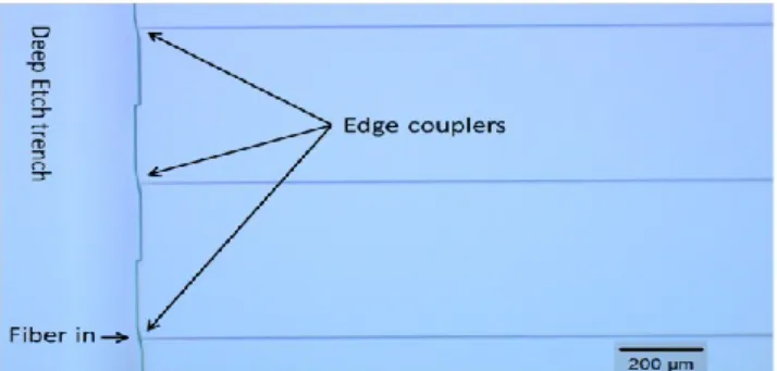
Figure 3 - Edge-coupling via inverted tapers tips of 160 nm ensuring coupling over a wide spectral window for nonlinear tests. Deep-etch trench profile (including 8° off-normal coupling facets) is to reduce feedback to fibers.
sources. As opposed to light thermal emission, these are highly coherent. In nonlinear waveguides, the intensity-dependent refractive index leads to SPM upon the propagation of short optical pulses and the generation of spectral continuum via its Kerr nonlinearity. The equation describing the related nonlinear phase shift is as follows:
∆𝜑𝑚𝑎𝑥= 𝛾𝑃𝐿𝑒𝑓𝑓 (1),
where 𝑃 is the coupled peak power, 𝛾 is the nonlinear parameter. It is related to the nonlinear index n2 through the
expression 𝛾=𝜔𝑛2
𝑐𝐴𝑒𝑓𝑓 , where 𝜔 is the angular frequency, 𝑐 is the
speed of light and 𝐴𝑒𝑓𝑓 is the effective area The effective length
𝐿𝑒𝑓𝑓 is given by 𝐿𝑒𝑓𝑓 = 1−𝑒−𝛼.𝐿
𝛼 . Depending on the linear
propagation loss 𝛼, Leff converges towards Lmax=1/ as a
function of the waveguide length (𝐿). By using the measured propagation losses, we estimate Leff to be 1.43 cm for our
2.1-cm-long single-mode waveguides, i.e., 56% of Lmax (2.55 cm),
meaning that by using longer waveguides we could get more SPM and a wider spectral broadening for a given input power and pulse duration. The efficiency in the continuum generation is naturally limited by linear and nonlinear losses. In our case, the latter such as two- or three-photon absorption are negligible, as attested by the linear transmission of our waveguides, even at high pump powers.
When a pulse passes through the silicon nitride waveguide, the material intensity-dependent nonlinear index produces blue-shifted spectral components on the trailing edge and red-blue-shifted spectral components on the leading edge of the optical pulse envelope. As the process accumulates along the waveguide, the pulse gets spectrally broadened, giving rise to a frequency continuum. Edge-coupling (1.2 dB coupling losses) via inverted tapers - as shown in Fig. 3 - was used in order to perform extensive nonlinear optical characterization over a large wavelength span in the 1.55 µm region. Using an external fiber-based laser followed by an erbium-doped fiber amplifier (EDFA), optical pulses of 2-ps duration with peak powers ranging from a few to hundreds of Watts at a repetition rate of 20 MHz were injected into the single-mode 2.1-cm-long silicon nitride waveguides (750 nm × 730 nm cross-section, =1.7 dB/cm). No fusing of waveguides nor degradation of the spectral broadening over time was observed. Experimental results are illustrated in Fig. 4(a). As shown, by increasing the coupled peak pump power, Kerr nonlinearity can be leveraged into a SPM process capable to generate a wide-spanning
Figure 4 - Spectral broadening of picosecond pulses via Kerr self-phase modulation (SPM) leading to the generation of a frequency continuum between 1515 - 1575 nm. (a) Spectral broadening at the Si3N4 waveguide output. (b)
Spectral broadening measured at the fiber output (i.e., before Si3N4 waveguide
input).
Figure 5 - Idler-signal degenerate four-wave mixing obtained in the silicon nitride waveguides. A 𝛄-factor in straight waveguides about 7 mm long point out to a 𝛄 -factor of 2.8 𝐖−𝟏𝐦−𝟏, while the continuous wave conversion efficiency is of -39 dB for 𝐋𝐞𝐟𝐟= 𝟎. 𝟔𝟑 𝐜𝐦 and coupled pump power of 28 dBm (20 dB attenuator is added at the output of the waveguide in order to protect the optical spectrum analyzer).
continuum of new optical frequencies around the 1543 nm pump wavelength. Note that on this plot, there is a non-negligible contribution of SPM arising in the EDFA used to amplify the pulsed laser signal as well as in the subsequent 7-m-long silica fiber crossed by the pump pulses before they reach the waveguide. The contribution of the EDFA to the spectral broadening is independent of the pump power though, since the latter is varied through the use of an attenuator placed after the amplifier. To clarify the relative contribution of the 7-m-long input fiber and Si3N4 waveguide to the overall SPM response,
we measured the spectrally broadened spectrum at the end of the input fiber, before injection into the waveguide as shown in Fig. 4(b). We also determined the nonlinear parameter of our silicon nitride waveguides by performing independently four-wave mixing measurements between slightly spectrally detuned continuous-wave pump and probe signals injected into a 7-mm-long single-mode Si3N4 waveguide via grating couplers. The
four-wave mixing conversion efficiency of our waveguide follows the equation (2):
𝜂 = 𝑃𝑖𝑑𝑙𝑒𝑟
𝑃𝑠𝑖𝑔𝑛𝑎𝑙= (𝛾𝑃𝐿𝑒𝑓𝑓) 2 (2),
The dispersion effects are neglected in (2) due to the small pump-probe detuning (1 nm) and dispersion of the waveguide (-315 ps/nm/km by finite element calculations). From Fig. 5, where the spectrum is normalized with respect to the input/output grating couplers losses, considering 𝐿𝑒𝑓𝑓 =0.63 cm
and P=28 dBm (coupled pump power) we can derive the nonlinear parameter 𝛾, which is equal to 2.8 𝑊−1𝑚−1 and
deduce the nonlinear index, which is equal 3.6 × 10⁻¹⁵𝑐𝑚2. 𝑊−1 (𝐴
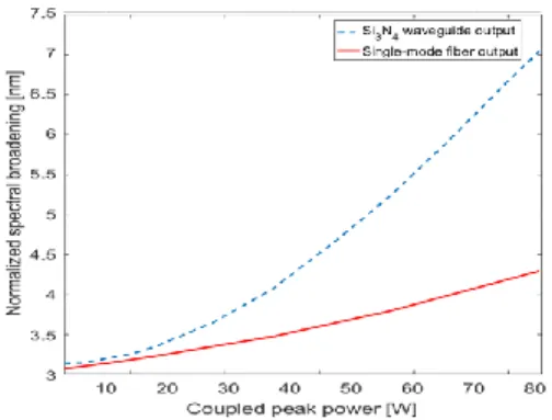
Figure 6 - Comparison between the normalized spectral broadening at the silicon nitride output and the single-mode fiber output.
and pump signals are multiplexed in a short-length single-mode fiber before entering into the silicon nitride waveguide so we can say that the contribution of the fiber in the four-wave mixing is negligible.
V. DISCUSSION
The nonlinearity of the silicon nitride obtained using the process presented below is slightly higher than obtained when 1200 °C annealing is applied (2.5 × 10⁻¹⁵ 𝑐𝑚2. 𝑊−1) [14].
Regarding the SPM measurements, after getting amplified by erbium-doped fiber, the pulse goes through seven-meter-long single-mode silica fiber with a nonlinear refractive index 𝑛2=
2.52 × 10⁻¹⁶𝑐𝑚2. 𝑊−1. To calculate the contribution of the
optical fiber in the continuum generation, the normalized spectral broadening as a function of the coupled peak power is calculated (see Fig. 6) using the equation:
∆𝜆 = (
∫𝑆(𝜆)(𝜆−𝜆0)2𝑑𝜆∫𝑆(𝜆)𝑑𝜆
)
1 2(3),
where 𝑆(𝜆) is the spectrum intensity as a function of wavelength. 𝜆0 is the central wavelength of the pulse
.
TheEquation (3) is used exclusively to calculate the contribution of the fiber. By taking the ratio (for 80 W) of the differences between the maximum and the minimum of the two curves we found that 29% of the broadening effect is in the fiber, which is consistent with the difference (×10) between the nonlinear index of the silicon nitride and silica, the effective area difference of the fiber and waveguide geometries, considering also that a long fiber (7 meters) is used before entering in the silicon nitride waveguide. Kerr nonlinearity could be then used to access SPM in such waveguides to generate 60-nm-spanning wavelength continuum across the C-band capable to provide hundreds of new available optical frequencies. Supercontinuum generation can be seen as a more valuable alternative to combs on the pathway towards heterogeneous cointegration of optical nonlinearities onto silicon photonic integrated circuits. In fact, different from Kerr combs generation demanding precise and ultra-stable resonant pumping lock over time [14]-[16], Kerr continua [13] are generally more stable, reducing the system complexity in addressing the stability over time.
VI. CONCLUSIONS AND PERSPECTIVES
We have demonstrated CMOS-compatible crack-free Si3N4
waveguides featuring full process compatibility with Si photonic integrated circuits paving the way to on-chip
Kerr-based broadband sources. In particular, a frequency continuum is generated over the C-band using silicon nitride films without extreme annealing, while a very well controlled optical quality is obtained by the fine tailoring of the tensile strain during the deposition process, preventing cracks from appearing with high-reproducibility across dies and wafers. This work paves the way toward a straightforward integration of broadband sources on existing Si-based photonics circuits and process including modulators, photodetectors, and (de-)multiplexers.
ACKNOWLEDGEMENTS
Acknowledgements: C. Monat acknowledges the support of the Institut Universitaire de France and the European ERC project GRAPHICS (648546) funded under H2020.
REFERENCES
[1] G. T. Reed, “The optical age of silicon,” Nature, vol. 427, pp. 595–596, 2004.
[2] M. Asghari and A. V. Krishnamoorthy, “Silicon photonics - Energy efficient communication,” Nat. Phot., vol. 5, pp. 268-270, May 2011. [3] B. Ben Bakir, et al., “Electrically driven hybrid Si/III-V Fabry-Pérot
lasers based on adiabatic mode transformers,” Opt. Exp., vol. 19, no. 11, pp. 10317–10325, 2011.
[4] M. Antelius, K. B. Gylfason, and H. Sohlström, “An apodized SOI waveguide-to-fiber surface grating coupler for single lithography silicon photonics,” Opt. Exp., vol. 19, pp. 3592-3598, 2011.
[5] L. Liao, D. Samara-Rubio, M. Morse, A. Liu, D. Hodge, D. Rubin, U. Keil, and T. Franck, “High speed silicon Mach-Zehnder modulator,” Opt.
Exp., vol. 13, pp. 3129-3135, 2005.
[6] L. Vivien, et al., “High speed and high responsivity germanium photodetector integrated in a Silicon-On-Insulator microwaveguide,” Opt.
Exp., vol 15, pp. 9843-9848, 2007.
[7] W. Bogaerts, et al., “Silicon-on-insulator spectral filters fabricated with CMOS technology,”IEEE. J. Sel. Topics in quantum Electron.vol. 16, no. 1, pp. 33,44, Jan.-Feb., 2010.
[8] G. Morthier, T. Spuesens, P. Mechet, G. Roelkens, and D.Van Thourhout, "InP Microdisk Lasers Integrated on Si for Optical Interconnects,"IEEE.
J. Sel. Topics in quantum Electron ., vol. 21, no. 6, pp. 359-368, 2015
.
[9] C. Sciancalepore, B. B. Bakir, S. Menezo, X. Letartre, D. Bordel and P. Viktorovitch, "III-V-on-Si Photonic Crystal Vertical-Cavity Surface-Emitting Laser Arrays for Wavelength Division Multiplexing," in IEEE
Photon. Tech. Lett, vol. 25, no. 12, pp. 1111-1113, June15, 2013.
[10] H. Duprez, et al., “1310 nm hybrid InP/InGaAsP on silicon distributed feedback laser with high side-mode suppression ratio”, Opt. Exp. ,Vol. 19, pp.8489-8497, 2015 .
[11] T. Ferrotti, et al., “Co-integrated 1.3µm hybrid III-V/silicon tunable laser and silicon Mach-Zehnder modulator operating at 25Gb/s,” Opt. Exp. ,Vol. 24, 30379-30401 ,2016.
[12] C.-H. Chen, et al.,“A comb laser-driven DWDM silicon photonic transmitter based on microring modulators,” Opt. Exp., vol. 23, pp. 21541-21548, 2015.
[13] H. Hu et al., “Single-Source AlGaAs Frequency Comb Transmitter for 661 Tbit/s Data Transmission in a 30-core Fiber,” in proc. OSA CLEO, pp. JTh4C-1, 2016.
[14] J. S. Levy, et al., “CMOS-compatible multiple-wavelength oscillator for on-chip optical interconnects”Nat. Phot., vol. 4, pp. 37-40, 2010.
[15] K. Luke, A. Dutt, C. B. Poitras, and M. Lipson, “Overcoming Si3N4 film
stress limitations for high quality factor ring resonators” Opt. Exp., vol. 21, no. 19, pp. 22829-22833, 2013
[16] M. H. Pfeiffer, et al., “Photonic Damascene process for integrated high-Q microresonator based nonlinear photonics”, Optica, vol. 3, no. 1, pp. 20-25, 2016.