Publisher’s version / Version de l'éditeur:
Journal of the Electrochemical Society, 152, 8, pp. F101-F106, 2005
READ THESE TERMS AND CONDITIONS CAREFULLY BEFORE USING THIS WEBSITE. https://nrc-publications.canada.ca/eng/copyright
Vous avez des questions? Nous pouvons vous aider. Pour communiquer directement avec un auteur, consultez la première page de la revue dans laquelle son article a été publié afin de trouver ses coordonnées. Si vous n’arrivez pas à les repérer, communiquez avec nous à PublicationsArchive-ArchivesPublications@nrc-cnrc.gc.ca.
Questions? Contact the NRC Publications Archive team at
PublicationsArchive-ArchivesPublications@nrc-cnrc.gc.ca. If you wish to email the authors directly, please see the first page of the publication for their contact information.
NRC Publications Archive
Archives des publications du CNRC
This publication could be one of several versions: author’s original, accepted manuscript or the publisher’s version. / La version de cette publication peut être l’une des suivantes : la version prépublication de l’auteur, la version acceptée du manuscrit ou la version de l’éditeur.
For the publisher’s version, please access the DOI link below./ Pour consulter la version de l’éditeur, utilisez le lien DOI ci-dessous.
https://doi.org/10.1149/1.1939087
Access and use of this website and the material on it are subject to the Terms and Conditions set forth at
Annealing effects on the chemical configuration of uncapped and
(poly-Si)-capped HfOxNy film deposited on Si(001)
Couillard, M.; Lee, M. -S.; Landheer, D.; Wu, X.; Botton, G. A.
https://publications-cnrc.canada.ca/fra/droits
L’accès à ce site Web et l’utilisation de son contenu sont assujettis aux conditions présentées dans le site LISEZ CES CONDITIONS ATTENTIVEMENT AVANT D’UTILISER CE SITE WEB.
NRC Publications Record / Notice d'Archives des publications de CNRC:
https://nrc-publications.canada.ca/eng/view/object/?id=049edb26-8881-4602-9212-cab32a256223
https://publications-cnrc.canada.ca/fra/voir/objet/?id=049edb26-8881-4602-9212-cab32a256223
Annealing Effects on the Chemical Configuration of Uncapped
and (Poly-Si)-Capped HfO
xN
yFilms Deposited on Si(001)
M. Couillard,a M.-S. Lee,bD. Landheer,c,
*
X. Wu,cand G. A. Bottona,za
Brockhouse Institute for Materials Research, McMaster University, L8S 4M1 Hamilton, Canada b
Department of Materials Science and Engineering, University of Toronto, M5S 3E4 Toronto, Canada c
Institute for Microstructural Sciences, National Research Council of Canada, K1A 0R6 Ottawa, Canada
We use spatially resolved spectroscopy in a scanning transmission electron microscope to study the thermal stability of the HfOxNy/Si共001兲 system with and without an in situ capping layer of silicon. The films were deposited by metallorganic chemical
vapor deposition using the amide precursor tetrakis共diethylamido兲hafnium with NO as the oxidant. A SiOxNyinterfacial layer
共⬃1.8 nm兲 is observed at the HfOxNy/substrate interface for films directly exposed to air. In addition, the N loss in the HfOxNy
film for the uncapped sample is significant. In contrast, in situ capping is found to reduce the thickness of the interfacial layer and to keep the N content in the final dielectric film high. The capped HfOxNyfilms are quasi-amorphous, whereas uncapped films are
polycrystalline following exposure to air. Oxinitridation at both interfaces is observed following a rapid thermal annealing process 共900°C in N2for 30 s兲 of the capped HfOxNyfilm. However, the interfacial layers remain thin 共⬃1 nm兲 and a significant amount
of N is present in the HfOxNyfilm. The rapid thermal annealing leads to the partial crystallization of the HfOxNyfilm and the Si
capping layer. No Hf silicate is detected on a scale of ⬃6 Å in the electron energy loss spectroscopy analysis. © 2005 The Electrochemical Society. 关DOI: 10.1149/1.1939087兴 All rights reserved.
Manuscript submitted November 22, 2004; revised manuscript received February 16, 2005. Available electronically July 7, 2005.
Hafnium oxide 共HfO2兲 has been proposed as an alternative
high-k dielectric to SiO2 for future complementary
metal-oxide-semiconductor 共CMOS兲 devices.1However, HfO2thin films have a
low crystallization temperature2,3and a high oxygen permeability,4 which causes the formation of a detrimental SiO2 layer at the Si
substrate interface when the dielectric film is exposed to air. In addition, there is a concern about the possible formation of Hf sili-cate and silicide at the interfaces.5Recently, the addition of N to form HfOxNy films has been proposed to improve stability.
6-10
The presence of N has been found to reduce the growth of the interfacial layer and to raise the crystallization temperature.6Furthermore, a study on HfOxNy gate dielectrics prepared by reactive sputtering
reported an improved thermal and electrical stability, which was attributed to Si-N bonds at the interface with the substrate.8 How-ever, recent results have indicated that oxidation can result in a significant loss of N in the HfOxNy films.10 Oxidation can be
avoided if the dielectric film is capped with a material that prevents the diffusion of oxygen11-13; hence, a capping layer may prevent the replacement of N in HfOxNyby O from the atmosphere. The
com-patibility of the high-k film with the capping layer remains an im-portant issue,14and the chemistry of the gate stack, especially at the interfaces, needs to be explored. In particular, understanding the influence of capping and annealing on the distribution of N is es-sential for the incorporation of nitrated high-k films in CMOS fab-rication.
The characterization in this experiment has been performed with high-resolution transmission electron microscopy 共HR-TEM兲 along with spatially resolved spectroscopy and high-angle annular dark-field 共HAADF兲 imaging in a scanning TEM 共STEM兲. Depth profiles of elements are obtained from the simultaneous collection in STEM mode of signals from electron energy loss spectroscopy 共EELS兲 and energy-dispersive X-ray spectroscopy 共EDS兲. Moreover, EELS analysis of the energy loss near-edge structures 共ELNES兲, which provide information on the surrounding of excited atoms, allows the mapping of phases rather than just elements. EELS has previously been applied to the study of several high-k films, including HfO2,15
Gd2O3,16 Sc2O3,17 Y2O3,12 La2O3,18 Al2O3,19 Hf silicate,20 Zr
silicate,21and Gd and La silicate.22In the EELS-STEM approach, the analysis region for a profile is directly selected from a high-resolution HAADF-STEM image, which provides contrast based on the atomic number. The local chemical and electronic information
extracted from simultaneously recorded spectra of EELS and EDS can be correlated with the structural information contained in HAADF-STEM images.23
In this work, we investigate the stability of uncapped and 共poly-Si兲-capped HfOxNy films deposited on a Si共001兲 substrate by
met-allorganic chemical vapor deposition 共MOCVD兲 using the amide precursor tetrakis共diethylamido兲hafnium 共TDEAH兲, 关共C2H5兲2N兴4Hf
with NO as the oxidant. In particular, we trace the distribution of nitrogen and oxygen before and after a rapid thermal annealing 共RTA兲 process. This study complements previous X-ray photoelec-tron spectroscopy 共XPS兲 investigations on uncapped HfOxNy
films.6,24The EELS analysis presented here confirms that the expo-sure of uncapped HfOxNyfilms to air leads to the oxinitridation of
the substrate and the loss of N in the dielectric film. In situ capping is found to prevent oxidation of the sample and thus to reduce growth of the SiOxNy interfacial layer. The N content in capped
HfOxNy films is also higher. RTA 共900°C, in N2 for 30 s兲 of the
capped film results in oxinitridation of both the 共HfOxNy/substrate兲
and the 共HfOxNy/capping layer兲 interface. The diffusion of excess O
and N in the dielectric films is thought to be responsible for this process. The resulting gate stack configuration, including the thin interfacial layers, is Si 共substrate兲/SiOxNy/HfOxNy/SiOxNy/Si
共cap-ping layer兲.
Experimental
p-Type Si共001兲 substrates with a resistivity of 0.035-0.065 ⍀ cm were given a HF-last RCA clean just prior to their introduction into an ultrahigh vacuum system, which comprises a low-pressure MOCVD chamber, an in situ XPS system, and a rapid postdeposition annealing 共PDA兲 chamber. The vacuum system also contains a rod-fed electron-beam evaporator for the deposition of amorphous silicon films. For the deposition of the hafnium oxyni-tride films by MOCVD, a 0.1 M solution of TDEAH dissolved in octane was introduced with Ar carrier gas into the chemical vapor deposition 共CVD兲 chamber with the vaporizer and gas distribution system held at 150°C. Si substrates were held at a temperature of 400°C during deposition, and the NO oxidant gas was introduced into the CVD chamber at a pressure of 11 mTorr through a separate gas introduction ring. The oxidant was introduced 5-10 min prior to film deposition with the substrate held at 500°C, for sample A, and at 400°C, for samples B and C. In situ XPS measurements confirm that for both temperatures a thin 共⬃0.4 nm兲 buffer layer with equal concentrations of N and O forms on the Si substrate. They also show that this thickness saturates in 1-2 min and is not sensitive to
oxi-*Electrochemical Society Active Member.
z
dation time in the 5-10 min range. Separate precursor and oxidant pulses were employed during the deposition of ⬃5 nm thick films, with intervening nitrogen flushing steps to minimize carbon con-tamination. After deposition the films were transferred in ultrahigh vacuum 共UHV兲 to the PDA chamber and annealed for 1 s at 800°C while the pressure remained ⬍10−7Torr. The capping of the
dielec-tric films for sample B and C was carried out after the PDA in two steps. First, following the anneal, ⬃20 nm of amorphous Si was deposited in situ using the E-beam evaporator. The samples were then taken out of vacuum at room temperature and a further ⬃200 nm of poly-Si was deposited in a separate chamber using low-pressure CVD 共LPCVD兲 at 600°C. The temperature reached in the latter process partially crystallized the a-Si layer initially depos-ited. For sample C, a further RTA was carried out at 900°C for 30 s in N2atmosphere.
The TEM characterization was carried out with a JEOL 2010F TEM/STEM with a Schottky field emission gun and operated at 200 keV. The microscope is equipped with a Gatan Tridiem energy filter and an Oxford Instruments 共atmospheric thin window兲 EDS. The cross-section samples A, B, and C 共see Table I兲 were prepared by tripod polishing25and low-energy 共2 keV兲 ion milling. The im-ages and the profiles were acquired with the Si substrate oriented along the 具110典 plane. The HAADF imaging and the spatially re-solved spectroscopy were performed with a STEM probe size of approximately 2-3 Å. The angle of convergence was 10 mrad and the acceptance angle was 50 mrad for both HAADF imaging and EELS.
The chemical characterization was performed by simultaneously collecting the signals from EELS and EDS while the probe was scanned across the interfaces and the dielectric film. DigitalMicro-graph software from Gatan was used for the EELS acquisition and also the EDS acquisition through an interface with Inca software from Oxford Instruments. The sampling for all the profiles is be-tween 0.2 and 0.8 nm, and the acquisition time varied bebe-tween 1 and 4 s. A small spatial drift was observed and corrected by assuming a constant rate and direction, which were deduced from HAADF im-ages taken before and after the spectra recording. The drift-corrected linescan was then converted to a depth profile normal to the gate stack. In the EDS spectrum, the Si K-peaks and the Hf M-peaks overlap; and the signal for each element was extracted using a mul-tiple linear least-squares 共MLLS兲 fit of reference spectra obtained from principal component analysis 共PCA兲. The MLLS fitting was performed with the routine available in the DigitalMicrograph envi-ronment. For the PCA, the eigenvectors were obtained from MatLab routines and a spectrum image was reconstructed following the method described in Ref. 26, which was implemented in the DigitalMicrograph environment. In EELS spectra, the background subtraction was performed with a power-law function extrapolated from the pre-edge region. The extraction of the N K edge 共401 eV兲 signal was rendered more difficult by the presence of the Hf N2,3
edge 共380 eV兲 and was therefore performed using a 10 eV back-ground window before the N K edge onset and a second backback-ground window just before the O K edge 共⬃532 eV兲 onset.
Results and Discussion
HR-TEM images 共Fig. 1兲 for the samples with deposition condi-tions summarized in Table I clearly show the difference in the thick-ness of the interfacial layer, which is estimated to be around 1.8 nm for sample A 共Fig. 1a兲, 0.8 nm for sample B 共Fig. 1b兲 and 1 nm for sample C 共Fig. 1c兲. For the uncapped sample, the exposure to air led to the formation of a relatively thick interfacial layer. The growth of the interfacial layer has previously been attributed to the diffusion of atomic oxygen through the dielectric films. The diffusion of O is rate-limited and slows down with the growing interfacial layer.27In situcapping of the HfOxNy film reduces the thickness of the
inter-facial layer. Figure 1 also shows that the top interface of the capped HfOxNyfilms is rough. A first inspection indicates that the images of
the capped dielectric film 共sample B兲 do not show clear periodicity, but the speckle is not fully uniformed as expected for amorphous layers. We therefore associate the structure to what has been labeled quasi-amorphous.15 In contrast, the uncapped film 共sample A兲 is polycrystalline. Thus, the exposure to air at room temperature rather than the PDA process appears responsible for the partial crystalliza-tion of the uncapped HfOxNyfilm. The RTA in N2atmosphere of the
capped dielectric film 共Fig. 1c, sample C兲 induces the partial crys-tallization of both the HfOxNyfilm and the Si capping layer.
Figure 2 shows elemental profiles for the three samples. The profiles of Hf and O have been normalized to their maximum value. The N profiles have been normalized with respect to O using cross sections calculated from the Hartree-Slater model. The N distribu-tion for sample A peaks inside the SiOxNy interfacial layer and the
quantity of N remaining in the HfOxNy film is low. The element
profiles of Fig. 2b indicate that most of the N remains inside the capped HfOxNyfilm. Moreover, the profiles show that the total N/O
ratio is higher for sample B than for sample A. By preventing the exposure of the film to air, the capping layer suppresses the absorp-tion and diffusion of O impurities from the ambient and by conse-quence reduces the interfacial SiOxNy growth. The observed
inter-facial layer for sample B 共Fig. 2b兲 may be due partly to the formation of a buffer layer from the NO oxidant introduced prior to the precursor and partly because of migration during the PDA pro-cess of expro-cess N and O contained in the dielectric film.
The profile for sample C 共Fig. 2c兲 displays a reduction in the N and O intensity near the center of the HfOxNyfilm. Such a reduction
in elemental profiles extracted from EELS can sometimes be attrib-uted to layers containing heavy elements.23In our case, however, the ratio of the thickness t over the mean-free path taken on the Si substrate is lower for the profiles of Fig. 2c 共t/ ⬃ 0.4兲 than for Fig. 2b 共t/ ⬃ 0.7兲. Thus, the reduction in intensity would have been more pronounced for the profiles of Fig. 2b. We therefore associate the reduction in signal to the migration during the RTA process 共900°C in N2for 30 s兲 of excess N and O in the HfOxNy
film toward the interfaces. Moreover, the N/O ratio taken at the center of the HfOxNyfilm is lower for sample C than for sample B,
implying that more N atoms than O atoms have diffused. The
ox-Table I. Description of three processes included in the prepara-tion of the three samples: the PDA, the in situ capping, and the RTA.a
Sample PDA In situcapping RTA
A 800°C, 1 s, in vacuum -
-B 800°C, 1 s, in vacuum ⬃20 nm a-Si -C 800°C, 1 s, in vacuum ⬃20 nm a-Si 900°C, 30 s, in N2 aA second capping layer of poly-Si 共⬃200 nm兲 was deposited on
sample B and C in a separate chamber before the RTA. The tempera-ture of 600°C reached in the latter process partially crystallizes the
first a-Si capping layer. Figure 1.HR-TEM images for the three samples described in Table I: 共a兲 A, 共b兲 B, and 共c兲 C.
F102 Journal of The Electrochemical Society, 152 共8兲 F101-F106 共2005兲 F102
initridation of both interfaces 共with the substrate and the capping layer兲 is also confirmed below in the analysis of the near-edge struc-ture obtained by EELS.
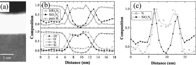
Figure 3a shows a HAADF-STEM image for sample A. The interfacial layer appears as a darker band between the HfOxNyfilm
and the substrate. Oxygen K edges from EELS spectra are presented in Fig. 3b for the HfOxNyfilm 共top兲 and the SiOxNyinterfacial layer
共bottom兲 phases. The onset and the shape of the edge for the two phases are distinct. The profile of phases shown in Fig. 3c is ob-tained from a MLLS fit of the experimental spectra at each STEM probe position to the reference spectra of Fig. 3b. The profiles of HfOxNy and SiOxNyphases 共top兲 are consistent with the elemental
profiles 共bottom兲. The comparison of the profiles also indicates that the ratio of N and O appears not to be uniform in both HfOxNyand
SiOxNy. Changes in the ELNES of the O K edge in the oxynitride
layer as a function of the N content, however, could not be detected within the energy resolution available to our system.
The EELS spectra for the Si L2,3 edge shown in Fig. 4a were
taken from sample A on the Si substrate 共top兲 and the interfacial layer 共bottom兲. The onset of the near-edge structure at the interfacial layer is located at lower energy than for SiO2and at higher energy
than for Si3N4.28The position of the onset is explained by the
pres-ence of both N and O atoms as the first neighbors of Si atoms. This confirms that the interfacial layer is silicon oxynitride. Figure 4b illustrates the profiles for pure Si 共substrate兲 and SiOxNy obtained
for a MLLS fit to the reference spectra of Fig. 4a. The profiles focus on the interface between the substrate and the interfacial layer; the HfOxNyfilm is located on the right 共outside the profile兲. An
addi-tional component extracted with PCA using the method described in Ref. 26 shows a structure at the Si/SiOxNy interface. The variation
of the Si ELNES at this interface is associated mainly with a change in stoichiometry but may also be influenced by a possible change in the N/O ratio near the interface.
For the capped HfOxNy film 共sample B兲, the O K
near-edge analysis confirms the presence of a SiOxNy layer at the
共HfOxNy/substrate兲 interface. A second SiOxNy layer at the
共HfOxNy/capping layer兲 interface is also revealed, but only in some
of the phase profiles. The elemental profile of Fig. 2b is consistent with the presence of a second interfacial layer, because the O distri-bution extends into the poly-Si capping layer 共located to the right of the HfOxNyfilm in the profile兲. The absence of the second
interfa-cial layer in some profiles can be explained either by a low signal extracted from the MLLS fits 共i.e., below the noise level兲 or to the nonuniform nature of the second SiOxNylayer. The latter possibility
is consistent with the rough 共HfOxNy/capping layer兲 interface.
How-ever, the morphology of the second interfacial layer has not been fully characterized.
A HAADF-STEM image of a capped HfOxNy film following
RTA is shown in Fig. 5a. The elemental profiles for sample C 共Fig. 5b兲 show that both N and O have migrated away from the HfOxNy
film. The phase mapping of Fig. 5b confirms the oxynitridation at the interfaces with both the Si substrate and the Si capping layer. The resulting configuration is therefore present: Si 共substrate兲/SiOxNy/HfOxNy/SiOxNy/Si 共capping layer兲. For Fig.
5b, the Si L2,3edge 共⬃99 eV兲 and the O K edge 共⬃532 eV兲 were
included in the same EELS acquisition, allowing the simultaneous ELNES mapping of pure Si 共with the Si L2,3edge兲, SiOxNy 共with
both the Si L2,3edge and the O K edge兲, and HfOxNy共with the O K
edge兲. Because the SiOxNyinterfacial layer was too thin, the
refer-ence spectra for the MLLS fit were taken from sample A for the O K edge 共Fig. 3b兲 and for the Si L2,3edge 共Fig. 4a兲. The C K edge
共⬃284 eV兲 was also included in the same acquisition. Although it is possible that some carbon from the precursor remains in the dielec-tric film,29we could not detect any evidence of Hf-C bonds using PCA. For sample C, the shape of the Si L2,3 edge taken at the
capping layer is very similar to the one at the substrate. This is in contrast to sample B, where due to the smaller grain size in the gate, a broader first peak 共99 eV兲 in the Si L2,3 edge is detected. The
results confirm the HR-TEM observations 共Fig. 1兲 indicating that the RTA has induced partial crystallization of the capping layer.
Principal component analysis of the O K and the Si L2,3edges
indicates that the samples included no detectable amount Hf silicate 共or silicide兲 on the length scale of ⬃6 Å. A previous study on the 共poly-Si兲-capped HfO2/Si system also found, with a similar
ap-proach, no detectable Hf silicate intermixing.15Because of the dif-ference between the O K edge of HfO2and Hf silicate 共HfSiO4兲,30
the presence of silicate would show up as a structured residual in the MLLS fits or as an additional significant component in PCA. The significant drop of the Si signal 共extracted from EELS兲 in the HfOxNy film supports the finding that no silicate is present. The
Figure 2.Elemental profiles for the three samples described in Table I: 共a兲 A, 共b兲 B, and 共c兲 C. The Hf and O profiles are normalized with their maxi-mum value equal to 1. The N profile is normalized with respect to O using inelastic 共atomic兲 cross sections calculated from the Hartree-Slater model. The Si substrate is located on the left.
formation of silicate has previously been detected in HfO2/Si
systems.31However, in that case, the oxidation occurred after sputter deposition of Hf. The substrate temperature and the oxygen pressure during oxidation of Hf film have been found to be critical for the interfacial reactions, especially for silicate formation.32In Ref. 31, the presence of a nitrided layer on the Si substrate was found to reduce 共without preventing兲 the intermixing. In our case, the intro-duction of the NO oxidant gas prior to the Hf precursor creates a nitrided layer on the Si substrate. Moreover, the oxidation of the Hf film occurs during each cycle, which consists of 共N2, NO, N2,
pre-cursor兲 pulses. These growth conditions appear to prevent the for-mation of silicate.
The distribution of N in the gate stack, especially following nec-essary processing steps such as RTA, is critical to define the dielec-tric properties. The source of N in our sample preparation is from both the NO oxidant gas and the precursor. For the uncapped sample, a significant loss of N in the HfOxNyfilm is observed and a
relatively thick SiOxNy interfacial layer is formed at the substrate
interface. Similar observations were made on HfOxNy gate
dielec-trics prepared by reactive sputtering.10The loss of N in the film and the oxinitridation of the interfacial layer are attributed to the incor-poration of O in the film in exchange of O and N. Such a process was clearly demonstrated for AlON films, where annealing in18O2 led to the incorporation of18O in replacement for16O and N previ-ously existing in the film.33For capped samples, oxinitridation oc-curs for both the substrate and the capping layer, but the resulting interfacial layers are thinner than for uncapped samples. Further-more, no significant oxidation occurs and thus the total N/O ratio remains high.
In Ref. 15, an unintentional SiO2layer was observed at the top
interface of a HfO2film capped with a poly-Si electrode. The
addi-tion of a nitrided layer between the HfO2and the poly-Si was
pro-posed as a solution to this reaction layer. The N-Si bonds formed at a HfOxNy/Si interface were identified as a factor leading to an
in-creased thermal and electrical stability of high-k films.7In addition, SiOxNy has a slightly higher dielectric constant than SiO2and the
growth of a SiOxNylayer is slower.
34
Experiments where nitridation of the surface was performed prior to film deposition have also demonstrated that the incorporation of N produces a diffusion barrier.31,35 However, the observed SiOxNy layer at the
共HfOxNy/capping layer兲 interface is not as well defined as the
inter-facial layer at the 共HfOxNy/substrate兲 interface. The instability at the
interface may therefore critically affect the use of poly-Si in a first generation gate.
For capped samples, a large quantity of N remains inside the
HfOxNyfilm, even after RTA 共Fig. 5c兲. The low availability of O to
replace N in the dielectric films explains this result. We note
how-Figure 4. 共a兲 Si L2,3edge for the substrate 共top兲 and the interfacial layer 共bottom兲 obtained from sample A 共see Table I兲. 共b兲 Phase profiles of pure Si and SiOxNy. An additional component extracted from PCA is also included
in 共b兲.
Figure 3. 共a兲 HAADF-STEM image of an uncapped HfOxNyfilm 共sample A, see Table I兲. 共b兲 O K near-edge structure for the HfOxNyfilm 共top兲 and the
interfacial layer 共bottom兲. 共c兲 Phase profiles 共top兲 of HfOxNyand SiOxNy, and elemental profiles 共bottom兲 of Hf, O, and N. All profiles are normalized with their
maximum value equal to 1 and the Si substrate is located on the left.
F104 Journal of The Electrochemical Society, 152 共8兲 F101-F106 共2005兲 F104
ever that a small quantity of residual O in the RTA chamber might have diffused through the gate and replaced some N in the dielectric film. N has the effect of decreasing the mean Hf coordination in HfOxNy.
9
This is in contrast with SiOxNy, where N increases the
mean Si coordination. This difference has been explained.9by the fact that N tends to be in fourfold coordination when bonded to Hf, whereas it is threefold when bonded to Si. The authors of Ref. 9 associate the reduction in Hf coordination to HfOxNybeing a better
glass former and therefore having a higher crystallization tempera-ture than HfO2. Furthermore, the presence of N in high-k oxide films
also reduces the diffusion of impurities through the film.
Conclusions
In summary, HfOxNy films were deposited on Si共001兲 by
MOCVD using 关共C2H5兲2N兴4Hf with NO as the oxidant. The
stabil-ity of both uncapped and 共poly-Si兲-capped films was investigated. The local chemistry, in particular the nitrogen distribution, and the bonding environment of atoms were determined with spatially re-solved EELS and EDS collected simultaneously with a subnanom-eter resolution. The exposure of HfOxNy films to air results in the
replacement of nitrogen in the film by oxygen and in the formation of a SiOxNylayer 共⬃1.8 nm兲 at the near interface with the Si
sub-strate. The elemental profiles also suggest that the N/O ratio is not uniform across the HfOxNy film and the SiOxNy interfacial layer.
HR-TEM imaging indicates that the uncapped HfOxNyfilm is
poly-crystalline.
In contrast, no oxidation is detected for HfOxNyfilms capped in
vacuum. The 共poly-Si兲-capped dielectric film retains a significant quantity of nitrogen and the thickness of the oxinitride interfacial layer is much reduced. Thus, in situ capping is found to be necessary and efficient to control the interface composition. Furthermore, the HfOxNy film remains quasi-amorphous. An RTA 共900°C in N2for
30 s兲 of the capped dielectric film results in the migration of nitro-gen and, to a lesser extent, oxynitro-gen away from the film, leading to the oxinitridation of both interfaces with silicon 共substrate and cap-ping layer兲. However, the interfacial layers remain thin, which cru-cially affects the overall capacitance of the system. The presence of the nitrided layer between the high-k films and the silicon is ex-pected to be beneficial for the stability of the gate stack by acting as a diffusion barrier for different species 共e.g., O, Si, B兲. The N con-tent in the capped high-k films, even following RTA, remains high. A higher crystallization temperature and reduced diffusion of impu-rities is therefore expected. However, the capped film following RTA is polycrystalline, and further studies on the morphology of the film are needed. Further work on the electrical properties of the
resulting gate stack of Si 共substrate兲/SiOxNy/HfOxNy/SiOxNy/Si
共capping layer兲 is also required.
Acknowledgment
The authors thank NSERC for financial support of this work. They are grateful to Fred Pearson and Andy Duft for technical sup-port and maintenance of the facilities. One of the authors 共M.C.兲 acknowledges support from an NSERC fellowship. Facilities are supported by NSERC, Canada Foundation for Innovation and On-tario Innovation Trust.
McMaster University assisted in meeting the publication costs of this article.
References
1. G. D. Wilk, R. M. Wallace, and J. M. Anthony, J. Appl. Phys., 89, 5243 共2001兲. 2. H. Kim, P. C. McIntyre, and K. C. Saraswat, Appl. Phys. Lett., 82, 106 共2003兲. 3. M.-Y. Ho, H. Gong, G. D. Wilk, B. W. Busch, M. L. Green, P. M. Voyles, D. A.
Muller, M. Bude, W. H. Lin, A. See, M. E. Loomans, S. K. Lahiri, and P. I. Räisänen, J. Appl. Phys., 93, 1477 共2003兲.
4. A. S. Foster, A. L. Shluger, and R. M. Nieminen, Phys. Rev. Lett., 89, 225901 共2002兲.
5. S. Stemmer, J. Vac. Sci. Technol. B, 22, 791 共2004兲.
6. M. Lee, Z.-H. Lu, W.-T. Ng, D. Landheer, X. Wu, and S. Moisa, Appl. Phys. Lett.,
83, 2638 共2003兲.
7. K.-J. Choi, J.-H. Kim, and S.-G. Yoon, J. Electrochem. Soc., 151, G262 共2004兲. 8. C. S. Kang, H.-J. Cho, K. Onishi, R. Nieh, R. Choi, S. Gopalan, S. Krishnan, J. H.
Han, and J. C. Lee, Appl. Phys. Lett., 81, 2593 共2002兲.
9. G. Shang, P. W. Peacock, and J. Robertson, Appl. Phys. Lett., 84, 106 共2004兲. 10. J. F. Kang, H. Y. Yu, C. Ren, M.-F. Li, D. S. H. Chan, H. Hu, H. F. Lim, W. D.
Kang, D. Gui, and D.-L. Kwong, Appl. Phys. Lett., 84, 1588 共2004兲.
11. B. W. Busch, J. Kwo, M. Hong, J. P. Mannaerts, B. J. Sapjeta, W. H. Schulte, E. Garfunkel, and T. Gustafsson, Appl. Phys. Lett., 79, 2447 共2001兲.
12. S. Stemmer, D. O. Klenov, Z. Chen, D. Niu, R. W. Ashcraft, and G. N. Parsons,
Appl. Phys. Lett., 81, 712 共2002兲.
13. M. Kundu, N. Miyata, T. Nabatame, T. Horikawa, M. Ichikawa, and A. Toriumi,
Appl. Phys. Lett., 82, 3442 共2003兲.
14. D. C. Gilmer, R. Hegde, R. Cotton, R. Garcia, V. Dhandapani, D. Triyoso, D. Roan, A. Franke, R. Rai, L. Prabhu, C. Hobbs, J. M. Grant, L. La, S. Samavedam, B. Taylor, H. Tseng, and P. Tobin, Appl. Phys. Lett., 81, 1288 共2002兲.
15. G. D. Wilk and D. A. Muller, Appl. Phys. Lett., 83, 3984 共2003兲.
16. G. A. Botton, J. A. Gupta, D. Landheer, J. P. McCaffrey, G. I. Sproule, and M. J. Graham, J. Appl. Phys., 91, 2921 共2002兲.
17. G. A. Botton, E. Romain, D. Landheer, X. Wu, M.-Y. Wu, M. Lee, and Z.-H. Lu, in Silicon Nitride and Silicon Dioxide Thin Insulating Films, R. E. Sah, K. B. Sundaram, M. J. Deen, D. Landeer, W. D. Brown, and D. Misra, Editors, PV 2003-02, p. 251, The Electrochemical Society Proceedings Series, Pennington, NJ 2003兲.
18. S. Stemmer, J.-P. Maria, and A. I. Kingon, Appl. Phys. Lett., 79, 102 共2001兲. 19. R. F. Klie, N. D. Browning, A. R. Chowdhuri, and C. G. Takoudis, Appl. Phys.
Lett., 83, 1187 共2003兲.
20. N. Ikarashi, M. Miyamura, K. Masuzaki, and T. Tatsumi, Appl. Phys. Lett., 84, 3672 共2004兲.
21. D. A. Muller and G. D. Wilk, Appl. Phys. Lett., 79, 4195 共2001兲.
Figure 5. 共a兲 HAADF-STEM image of a capped HfOxNy/Si sample following RTA 共sample C, see Table I兲. 共b兲 Phase profiles 共top兲 and elemental profiles
共bottom兲. The signal for N, O, and Si was extracted from EELS and the signal for Hf was extracted from EDS. 共c兲 Profile of N and SiOxNy. The N profile in
共b兲 is normalized with respect to O using inelastic 共atomic兲 cross sections calculated from the Hartree-Slater model. Other profiles are normalized with their maximum value equal to 1. The Si substrate is located on the left in the profiles.
22. X. Wu, D. Landheer, T. Quance, M. J. Graham, and G. A. Botton, Appl. Surf. Sci.,
200, 15 共2002兲.
23. B. Foran, J. Barnett, P. S. Lysaght, M. P. Agustin, and S. Stemmer, J. Electron
Spectrosc. Relat. Phenom., In press.
24. M. Lee, D. Landheer, X. Wu, M. Couillard, Z.-H. Lu, and W.-T. Ng, Mater. Res.
Soc. Symp. Proc., 811, 7.2.1 共2004兲.
25. P. M. Voyles, J. L. Grazul, and D. A. Muller, Ultramicroscopy, 96, 251 共2003兲. 26. N. Bonnet, N. Brun, and C. Colliex, Ultramicroscopy, 77, 97 共1999兲.
27. B. W. Busch, W. H. Schulte, E. Garfunkel, T. Gustafsson, W. Qi, R. Nieh, and J. Lee, Phys. Rev. B, 62, R13290 共2000兲.
28. K. Kimoto, K. Kobayashi, T. Aoyama, and Y. Mitsui, Micron, 30, 121 共1999兲. 29. J. Schaeffer, N. V. Edwards, R. Liu, D. Roan, B. Hradsky, R. Gregory, J. Kulik, E.
Duda, L. Contreras, J. Christiansen, S. Zollner, P. Tobin, B.-Y. Nguyen, R. Nieh, M. Ramon, R. Rao, R. Hegde, R. Rai, J. Baker, and S. Voight, J. Electrochem. Soc.,
150, F67 共2003兲.
30. D. W. McComb, A. J. Craven, D. A. Hamilton, and M. MacKenzie, Appl. Phys.
Lett., 84, 4523 共2004兲.
31. P. D. Kirsch, C. S. Kang, J. Lozano, J. C. Lee, and J. G. Ekerdt, J. Appl. Phys., 91, 4353 共2002兲.
32. J.-H. Lee, N. Miyata, M. Kundu, and M. Ichikawa, Phys. Rev. B, 66, 233309 共2002兲.
33. K. P. Bastos, R. P. Pezzi, L. Miotti, G. V. Soares, C. Driemeier, J. Morais, I. J. R. Baumvol, C. Hinkle, and G. Lucovsky, Appl. Phys. Lett., 84, 97 共2004兲. 34. N. Bassim, V. Craciun, J. Howard, and R. K. Singh, Appl. Surf. Sci., 205, 267
共2003兲.
35. K. P. Bastos, J. Morais, L. Miotti, G. V. Soares, R. P. Pezzi, R. C. G. da Silva, H. Boudinov, I. J. R. Baumvol, R. I. Hegde, H.-H. Tseng, and P. J. Tobin, J.
Electro-chem. Soc., 151, F153 共2004兲.
F106 Journal of The Electrochemical Society, 152 共8兲 F101-F106 共2005兲 F106