HAL Id: tel-01609934
https://tel.archives-ouvertes.fr/tel-01609934
Submitted on 4 Oct 2017
HAL is a multi-disciplinary open access
archive for the deposit and dissemination of sci-entific research documents, whether they are pub-lished or not. The documents may come from teaching and research institutions in France or abroad, or from public or private research centers.
L’archive ouverte pluridisciplinaire HAL, est destinée au dépôt et à la diffusion de documents scientifiques de niveau recherche, publiés ou non, émanant des établissements d’enseignement et de recherche français ou étrangers, des laboratoires publics ou privés.
scale : routes for a possible integration as a new
nanostructuring technology
Sophie Böhme
To cite this version:
Sophie Böhme. Towards high-chi block copolymers at the industry scale : routes for a possible integra-tion as a new nanostructuring technology. Micro and nanotechnologies/Microelectronics. Université Grenoble Alpes, 2016. English. �NNT : 2016GREAT109�. �tel-01609934�
THÈSE
Pour obtenir le grade de
DOCTEUR DE LA COMMUNAUTE UNIVERSITE GRENOBLE
ALPES
Spécialité : Nanoélectronique et Nanotechnologies
Arrêté ministériel : 7 août 2006
Présentée par
Sophie Böhme
Thèse dirigée par Jumana Boussey
préparée au sein du LTM (CNRS / UJF-Grenoble 1 / CEA) dans l'École Doctorale EEATS
Towards High-
χ Block Copolymers at the
Industry Scale
– Routes for a Possible
Integration as a New Nanostructuring
Technology
Vers les opoly
res à lo s à forte i o pati ilit da s l’i dustrie –
des voies pour l'intégration en tant que nouvelle technologie de
nanostructuration
Thèse soutenue publiquement le 19 octobre 2016, devant le jury composé de :
Jérôme Plain
Professeur de l’U iversit de Te h ologie de Troyes, Président
Christophe Sinturel
Professeur de l’U iversit d’Orléans, Rapporteur
Olivier Soppera
Directeur de recherche, CNRS, IS2M, Mulhouse, Rapporteur
Karim Aissou
Chargé de recherche, CNRS, LCPO, Bordeaux, Examinateur
Jumana Boussey
Directrice de recherche CNRS, LTM, Grenoble, Directrice de thèse
Marc Zelsmann
Chargé de recherche, CNRS, LTM, Grenoble, Co-encadrant de thèse
Raluca Tiron
ii
First of all I would like to thank Olivier Joubert, director of the LTM, for giving me the opportunity to work at the LTM and the LabeX Minos directory for financing this thesis.
Furthermore, I would like to thank my Ph.D director Jumana Boussey for her support, encouragement and advice. I would also like to express my sincere gratitude to my advisor Marc Zelsmann for the continuous support of my Ph.D study and research, for his patience, motivation, and immense knowledge. His guidance helped me in all the time of research and writing of this thesis while giving me the freedom to explore my own ideas.
I would also like to thank the members of the thesis examination committee, Prof. Christophe Sinturel and Dr. Olivier Soppera for taking the time to referee the thesis, and Prof. Jérôme Plain (chairman of the committee) and Dr. Karim Aissou who agreed to be part of the jury.
I want also to express my gratitude to Raluca Tiron for her insightful comments, her help and encouragement.
A large thanks to all the colleagues at LTM that helped me with various problems regarding plasma etching, STEM or AFM imaging and everything else: Camille, Gilles, JH, Kevin, Laurent, Nathalie, Odile, Philippe, Seb. Great thanks goes also to Céline, Malou, Stéphanie and Sylvaine for all their help in bureaucracy, financial or other issues.
Further I want to thank everybody in the copo -team for sharing our passion (or was it?) for BCPs, the advice, support and the enriching discussions: Antoine, Cécile, Javier and Jérôme G.
Not to forget the colleagues that became friends during my time at the LTM and, without whom that time wouldn’t have been as much fun as it was. The long evenings that we spent chez Emile are unforgettable and I will definitely miss them: Anthony, Benoît, Jérôme D., Manu, Maxime, Michel, Nico, Olivier, Thibault and Tiphaine.
Last but not least I would like to thank Julien, without whom none of this would have happened, who always knew how to motivate and push me forward and my close friends and family who always believed in me and supported me, no matter what.
iv
The increasing cost and complexity of processes needed to keep up with the ever increasing demand for more powerful processors in the IC industry, lead to smaller and smaller feature sizes. Photolithography, once the workhorse for nanostructuration, reaches now its physical limits in terms of resolution. Other, alternative methods have thus to be found in order to continue producing more efficient integrated circuits, while keeping the production costs at a reasonable level. The combination of conventional photolithography and directed self-assembly of block copolymers (BCP) seems to be one promising alternative. Block copolymers have the unique property to phase separate at the nanometer scale driven by the chemical incompatibility (described by the Flory-Huggins interaction parameter χ) of the blocks. This way, when brought onto a substrate, structures like spheres, cylinders or lamellar can be obtained and used as etching masks for nanostructuration. Probably the most used BCP is Polystyrene-b-Polymethylmethacrylate (PS-b-PMMA), which has been studied for over 20 years. PS-b-PMMA is a so called
low- χ BCP and can reach feature sizes not smaller than ̴ nm. The higher the incompatibility of the blocks (i.e. the higher the χ-value), the smaller the obtainable feature size. This thesis deals primarily with high-χ Polystyrene-b-Polydimethylsiloxane (PS-b-PDMS) block copolymers and evaluates its possible integration into IC industry. Processes are developed and optimized in view of their future application in industry. A common annealing method for high-χ block copolymers is solvent vapor annealing SVA , where the BCP layer is exposed to solvent vapors. Solvent molecules swell then the BCP layer, increasing the mobility of polymer chains and allowing long range ordering of the features. Although this method is widely used, it has never been reported on large scale production lines, for example on 300 mm wafers. The SVA is a very complex process that is sensitive to the environment and uses often toxic solvents. During this thesis, mechanisms of solvent vapor annealing are studied and safe solvents that are compatible with industrial environment are studied. Furthermore, alternative solutions for annealing high-χ BCPs without solvents are proposed. Blending the BCP with plasticizer molecules, for example, leads to rapid self-assembly with thermal annealing and the feasibility of this process was shown on 300 mm wafers.
Pattern transfer etching is a problematic step in IC nanostructuring. The smaller the features, the higher the aspect ratio, the more challenging the etching process. Different plasma etching procedures, all typically used in industrial gate etching processes, are studied on PS-b-PDMS. Challenging silicon features of down to 10 nm and aspect ratios of up to 6:1 are obtained.
Finally, a simple spin-coating process of metal-oxide inclusion on widespread PS-b-PMMA is introduced in which etch selectivity of the BCP is highly increased. PS-b-PMMA has the advantage of being studied by numerous research groups and the understanding of the BCP is very advanced. However, its etching quality for pattern transfer is very poor as to the poor etch selectivity between PS and PMMA. Complicated
v
etch contrast is considerably enhanced and the pattern transfer can be obtained in one single step of dry etching.
vi
La complexité et le coût croissant des processus nécessaires pour fabriquer les processeurs de plus en plus puissants de l'industrie microélectronique conduit à des structures de plus en plus petites. La photolithographie, technologie clé pour la nanostructuration, atteint aujourd'hui ses limites en termes de résolution. Des méthodes alternatives doivent donc être trouvées afin de continuer à produire des transistors plus efficaces, tout en gardant les coûts de production à un niveau raisonnable. La combinaison de la photolithographie classique et de l'auto-assemblage de copolymères à blocs (CPB) semble être une alternative prometteuse. Les copolymères à blocs ont la propriété de créer une séparation de phases à l'échelle du nanomètre grâce à l'incompatibilité chimique (décrite par le paramètre d'interaction χ des blocs. De cette façon, lorsque cette séparation de phase est formée à la surface d’un substrat, des structures telles que des sphères, des cylindres ou des lamelles peuvent être obtenues et utilisées comme masques de gravure pour la nanostructuration. Le CPB le plus utilisé est probablement le Polystyrène-Polyméthacrylate de méthyle (PS-PMMA), qui a été étudié pendant plus de 20 ans. Le PS-PMMA est un CPB de faible χ et ne peut pas atteindre des tailles de structure inférieures à 12nm. Plus l'incompatibilité des blocs c’est-à-dire le χ est importante, plus la taille des structures possibles est petite. Cette thèse traite principalement le système Polystyrène-Polydiméthylsiloxane (PS-PDMS , un CPB de haute valeur de χ, et évalue son éventuelle intégration dans l'industrie de la microélectronique. Des procédés ont été développés et optimisés en vue de leur utilisation future dans l'industrie. Un procédé de recuit commun pour les "high-χ" est le recuit sous vapeur de solvant (RVS), où la couche de CPB est exposée aux vapeurs de solvants. Les molécules de solvant gonflent le CPB et augmentent ainsi la mobilité des chaînes de polymère, permettant l’organisation des structures à grande échelle. Bien que ce procédé soit largement utilisé, il n'a jamais été utilisé sur des lignes de production à grande échelle. Le RVS est un processus très complexe qui est sensible à l'environnement et utilise souvent des solvants toxiques. Au cours de cette thèse, des mécanismes de RVS sont étudiés et des solvants non-toxiques qui sont compatibles avec l'environnement industriel sont proposés comme alternative. Une autre solution pour le recuit de CPBs "high-χ" sans solvant est également proposée. En formulant la solution de CPB avec des molécules de plastifiant, un auto-assemblage rapide avec un simple recuit thermique est possible. La faisabilité de ce processus a été démontrée sur des tranches de silicium de 300mm de diamètre.
Le transfert des motifs par gravure est une étape importante et problématique en nanofabrication. Plus les tailles sont réduites, plus le facteur d'aspect est haut et le processus de gravure difficile. Des procédés de gravure par plasma différents, tous utilisés dans des procédés de gravure industriels, sont étudiés sur le matériau PS-PDMS. Des nanostructures de silicium de 10nm de large et des structures avec un rapport d'aspect de 6:1 ont été gravées avec succès.
vii
de recherche qui s’y intéresse. Cependant, ses performances en gravure pour le transfert des motifs est peu satisfaisant à cause de la faible sélectivité entre les blocs PS et PMMA. Des procédés de gravure compliqués en plusieurs étapes doivent être effectués afin de transférer les motifs de manière satisfaisante. En introduisant des sels métalliques de manière sélective dans l'un des blocs, le contraste de gravure est considérablement augmenté et le transfert du motif peut être obtenu en une seule étape de gravure plasma.
viii
Table of Abbreviations ... xii
Introduction ... 1
1.1 Photolithography ... 3
1.1.1 The Beginning of Integrated Circuit Production ... 3
1.1.2 Conventional Photolithography ... 4
1.1.3 193 Immersion Lithography ... 7
1.1.4 Extreme Ultraviolet Lithography ... 7
1.1.5 Double Patterning ... 7
1.2 Alternative Lithography Techniques ... 8
1.2.1 Nanoimprint ... 8
1.2.2 Block Copolymer Lithography ... 8
1.3 Directed Self-Assembly of Block Copolymers ... 9
1.3.1 Thermodynamics of Block Copolymers ... 9
1.3.2 Block Copolymer Thin Films ... 13
1.3.3 Large Area Orientation of BCPs ... 19
1.3.4 Application of Directed Self-Assembly in Nanomanufacturing ... 23
1.3.5 High-χ Block Copolymers ... 25
1.4 Motivation and Outline of the Thesis ... 28
References ... 30
Pattern Generation of Lines via Solvent Vapor Annealing of a Cylindrical PS-b-PDMS ... 39
2.1 Introduction ... 41
2.2 Experimental Details ... 42
2.3 Effect of Substrate Wetting on PS-b-PDMS (Mw=45.5kg/mol) ... 44
2.4 Graphoepitaxy and Solvent-Vapor Annealing of SD45 in SiArc/SOC Trenches ... 48
2.5 GISAXS in-situ Measurements of SVA on SD45 ... 55
2.6 Line Edge Roughness Measurements of SD45 ... 58
2.7 Conclusion ... 59
References ... 61
Pattern Generation of Lines and Dots via Thermal Annealing of PS-b-PDMS ... 65
ix
3.4 Graphoepitaxy and Application of SD45 on Large Area Surfaces ... 78
3.5 Conclusion ... 82
References ... 84
Pattern Generation of High Resolution Lines via Thermal Annealing of a Cylindrical PS-b-PDMS ... 87
4.1 Introduction ... 89
4.2 Experimental Details ... 89
4.3 Effect of Substrate Wetting on PS-b-PDMS (Mw=16kg/mol) ... 90
4.4 Solvothermal Annealing of SD16 on Silicon Graphoepitaxy Substrates ... 92
4.5 Thermal Annealing of SD16 on SiArc/SOC Graphoepitaxy Substrates ... 96
4.6 Line Edge Roughness Measurements of SD16 ... 97
4.7 Conclusion ... 99
References ... 100
DSA Pattern Transfer by Plasma Etching ... 105
5.1 Introduction ... 106
5.2 Experimental Details ... 109
5.3 Revelation: Etching PDMS, PS and SOC ... 113
5.4 HBr/O2 Pulsed Plasma Transfer Etching of SD45 on Thick SOC Layers... 116
5.5 SF6/CHF3/Ar Continuous Wave Plasma Transfer Etching of SD45 on Thin SOC Layers ... 118
5.6 Comparison of Pulsed and Continuous Wave Plasma on SD45 ... 119
5.7 Transfer Etching of SD16 ... 120
5.8 Conclusion ... 123
References ... 125
Extended Functionalities for Block Copolymer ... 129
6.1 General Introduction ... 131
6.2 Double Patterning of PS-b-PDMS ... 131
6.2.1 Introduction ... 131
6.2.2 Experimental Details ... 132
6.2.3 Nanomesh Formation with Double Patterning of SD45 ... 132
6.2.4 Nanomesh Formation with Double Patterning of SD16 ... 134
x
6.3.1 Introduction ... 137
6.3.2 Experimental Details ... 140
6.3.3 PS-b-PMMA Self-Assembly and Surface Reconstruction... 140
6.3.4 Metal Salt Inclusion and Pattern Transfer Etching ... 143
6.4 Conclusion ... 146
References ... 147
Conclusion and Perspectives ... 151
xii AFM Atomic force microscopy
ALD Atomic layer deposition
BCC Body centered cubic
BCP Block copolymer
CD Critical dimension
CDU Critical dimension uniformity
CW Continuous wave
Dh Hydrodynamic diameter
DIS Disordered
DLS Dynamic light scattering
DOA Diisooctyl adipate
DOA42 SD42+DOA
DOA45 SD45+DOA
DOS Dioctylsebacate
DOS42 SD42+DOS
DOS45 SD45+DOS
DPS Decoupled plasma source
DSA Directed self-assembly
ESRF European synchrotron radiation facility
EtOH Ethanol
EUV Extreme ultraviolet
FFT Fast Fourier transform
FIB Focused ion beam
finFET Fin field-effect transistor
GISAXS Grazing incident small angle X-ray scattering
GYR Gyroidal
HEX Hexagonal
HPL Hexagonally perforated lamellar HSP Hansen solubility parameter
IC Integrated circuit
ICP Inductively coupled plasma
ITRS International technology roadmap for semiconductors
L0 Natural period of BCP
LAM Lamellar
LER Line edge roughness
LTM Laboratoire de technologies de la microélectronique LWR Line width roughness
MH Maltoheptaose
N Degree of polymerization
NIL Nanoimprint lithography
xiii
PB Polybutadiene
PDMS Polydimethylsiloxane
PEO Polyethylene oxide
PFS Polyferrocenyldimethylsilane
PGMEA Propylene glycol methyl ether acetate
PI Polyisoprene
PLA Polylactid
PMMA Poly(methyl methacrylate)
PS Polystyrene
PtBS Poly-4-ter-butylstyrene
PTMSS Poly(para-trimethyl silystyrene)
RF Radio frequency
RT Room temperature
SCFT Self-consistent mean field theory SD16 PS-b-PDMS: Mw=16kg/mol, L0=20nm SD42 PS-b-PDMS: Mw=42kg/mol, L0=33nm SD45 PS-b-PDMS: Mw=45kg/mol, L0=35nm SEM Scanning electron microscopy SiArc Silicon antireflective coating SIS Sequential infiltration synthesis
SOC Spin-on-carbon
SOI Silicon on insulator SSL Strong segregation limit
STEM Scanning transmission electron microscopy
SVA Solvent vapor annealing
TA Thermal annealing
Tg Glass transition temperature
TGA Thermogravimetric analysis
VUV Vacuum ultra violet
WSL Weak segregation limit
XPS X-ray photoelectron spectroscopy χ Flory-Huggins interaction parameter
1
Introduction
3
1.1
Photolithography
1.1.1 The Beginning of Integrated Circuit Production
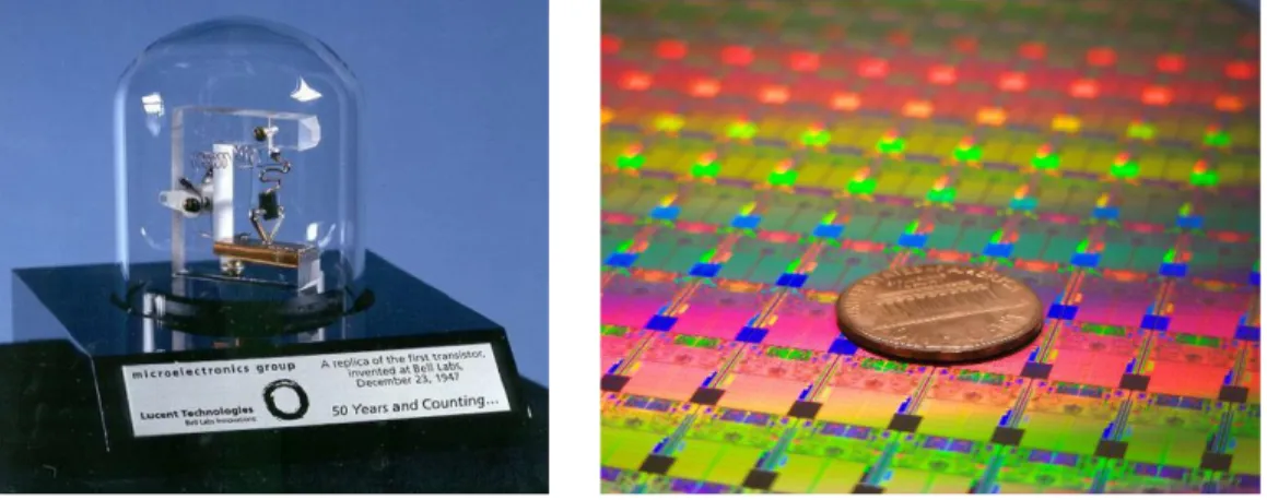
In the last decades, many efforts have been made in terms of miniaturization, cost, speed, power consumption and versatility concerning the silicon based integrated circuits (IC) industry. In 1947 the first microprocessor was commercialized by Intel and possessed about 2300 transistors. 1958 Jack Kilby invented the first integrated circuit at Texas )nstruments and by the ’ies one chip contained about transistors. Ever since, tremendous progress has been made and today’s microprocessors contain up to four billion transistors. To illustrate the evolution of transistor, Figure 1-1 shows a replica of the first transistor and a 300 mm wafer that contains hundreds of millions of transistors.
Figure 1-1: Comparison of the first transistor1 and today’s mm wafer containing hundreds of millions of transistors2
To build these kinds of processors a series of operations is performed on one piece of silicon, among the process steps are photolithography, etching or deposition. Each of these steps is performed by specialized equipment built by commercial companies. In order for the industry to advance, a roadmap, the so called International Technology Roadmap for Semiconductors (ITRS) was introduced over 20 years ago to anticipate the technological evolution and predict technological needs of the IC industry. With the help of this roadmap, industry was able to double the number of transistors per chip every 2 years, increasing processing power exponentially, while keeping the production cost constant. A schematic of this evolution is depicted in Figure 1-2 and was already predicted by Gordon Moore in 1965: it is known to us today as Moore’s law3. Today in 2016, the most powerful chips commercially available are at the 14 nm technology node, i.e., the typical half-pitch of a feature is approximately 14 nm. Prior to the 14 nm node was the 22 nm node, introduced in 2012, and next is supposed to be the 10 nm node in 2017.
4
Figure 1-2: Representation of Moore’s law 4
Even though Moore’s law has been true for the last years, it seems that technology evolution slows down. Indeed the technological complexity to decrease feature sizes becomes tremendous. The simple and classic photolithography, which was for a long time the microelectronics workhorse, reached its limits at feature sizes of approximately 45 nm due to light diffraction problems. In order to attain the 14 nm node, it was necessary to integrate complex lithography processes, whose prizes grow with decreasing feature size. In order to reduce the cost of nanostructuring, alternative lithography techniques have been introduced in recent years
1.1.2 Conventional Photolithography
Photolithography is a key step in the production of transistors and uses photoresists and light to transfer a geometric pattern from a mask onto a substrate. The parts of the resist that are exposed to light are chemically modified. With a chemical solution, a developer, either the exposed parts (positive resist) or those not exposed to light (negative resist) can be removed, creating an image of the initial pattern at the substrate surface. After developing the resist, the parts free of resist can be processed, while those covered with resist will be protected. That way the pattern can be transferred into the substrate. A schematic of the process is depicted in Figure 1-3
5
Figure 1-3: Schematic representation of the optical photolithography process
The simplest types of lithography are contact and proximity lithography. In contact mode the mask is in direct contact of the resist, limiting the lifetime of the mask and bringing a risk of contamination into the process. In proximity lithography, the mask is maintained at a certain distance of a few micrometers above the resist, limiting its resolution to the micrometer scale5. Further evolution of photolithography led to projection lithography. This technique avoids the direct contact of the mask and wafer, by projecting the pattern onto the photoresist via a refractive optical system, as depicted in Figure 1-4. As can be seen on the schematic, a projection lens is positioned between the photomask and photoresist which allows a demagnification of the pattern of at least 4x in most systems6. Projection optical photolithography is today’s most used type of nanopatterning.
6
Figure 1-4: Schematic representation of projection lithography6
The resolution of the obtained structures depends on the one hand on the material of the resist and on the other hand on the wavelengths that are used. The smaller the wavelength, the higher the possible resolution. Since the beginning of photolithography a great part of the whole photon spectrum was exploited for nanostructuration. In the beginning, when the feature sizes on transistors were as big as a few micrometers, wide spectrum lamp light was used. Since then, light sources used more and more powerful photons, passing by UV-light in the ’s with a wavelength of nm (G-line) to produce structures of 5 to 6 µm. In the late 198 ’s lithography moved on to nm )-line) and produced 1µm features. The next step, to sub-1µm structures was considered challenging but was obtained in the 1 ’s with deep UV-light at 248 nm and by 1993, 500 nm features were produced commercially. )n the ’s finally, the nm wavelength was introduced which is still today the main photolithography exposure technique in industry7,8. The relationship between wavelength and obtainable feature size becomes clear in the Rayleigh equation:
= �� Equation 1-1
Where CD is the critical dimension, the wavelength, NA the numerical aperture of the system’s lens and k1 is known as the resolution factor and accounts for all other process variables9. Besides using shorter wavelength, only the numerical aperture can be increased or k1 reduced in order to improve feature sizes. Continuous improvement of the lens systems has helped in the downscaling process of feature size but desired resolutions today are at 20 nm and below, whereas classic dry 193 nm lithography tools attain 90 nm resolution.
7
1.1.3 193 Immersion Lithography
193 nm immersion lithography (193i) has been introduced in IC manufactory in 2002 in order to attain the 45 nm technology node. In this technique the medium in which lithography takes place is changed from air to a liquid (usually purified water) with a higher refractive index10. The introduction of water into the gap between the final lens and wafer changes the optical paths of exposure light, decreasing the effective wavelength of 193 nm to 135 nm. This way the final resolution is improved, enabling the production of 45 nm node circuits.
1.1.4 Extreme Ultraviolet Lithography
Extreme ultraviolet (EUV) lithography uses light with an extreme small wavelength of 11 - 14nm. Most materials, including oxygen and nitrogen, absorb these short wavelengths, which is why EUV lithography machines must operate in vacuum. Also, the optical system, including mask and mirrors, must be coated by materials that are able to reflect the short wavelength light. Mirror materials composed of multilayers of silicon and molybdenum reach reflectivities of 60 - 70% in EUV11,12. In order to compensate for the power loss, extreme high power EUV sources are necessary. Due to the high cost and complexity of the system, EUV lithography is not yet used in IC manufacturing.
1.1.5 Double Patterning
Double or multiple patterning lithography has been introduced to bridge the gap between immersion lithography and the delayed readiness of EUV lithography and is now expected to be also used for the upcoming 10 nm node. The principle is based on the sequential exposure with immersion lithography so that a multiplication of feature density can be obtained. The integration of this concept avoids the investment into new equipment and materials, as immersion photolithography is already used in industry. However, due to the increased number of steps (successive lithography and etch), the reduction of the cost of ownership is not evident.
8
Numerous variations of this technique exist and one of the first was the litho etch litho etch process. Here two subsequent lithography and etching steps lead to the final density multiplication while in the litho freeze process, only one etching step is required. Here, two different masks are used to obtain two different lithography patterns. By freezing-in the first pattern, it is not affected during the second exposure13. These two processes are depicted in Figure 1-5. Apart from increased number of process steps, overlay and design issues make the implementation of double patterning for the 10 nm node very challenging14.
1.2
Alternative Lithography Techniques
1.2.1 Nanoimprint
Nanoimprint lithography was introduced in 1995 in order to propose a cost-effective, high-throughput alternative manufacturing process of nanopatterning in the sub-50 nm scale15. This alternative lithography technique uses thickness contrast rather than optical contrast in order to create nanostructures in thin film resists. The basic principle of the method is schematically represented in Figure 1-6. A mold is pressed onto a resist, creating a thickness contrast on the resist. By releasing the mold, a negative image is reproduced to scale. Remaining residues inside the compressed areas can be etched away by reactive ion etching (RIE) and the obtained structures can be transferred to the pattern, similarly to the obtained images in photolithography.
Figure 1-6: Schematic of the nanoimprint lithography process: first, the mold is pressed onto a resist in order to create a thickness contrast, then the mold is removed, and residue resist between features is removed by reactive ion etching Drawbacks of this technique are the high cost of the master mold when using decreased feature sizes as well as the high defectivity which is not compatible with industry expectations.
1.2.2 Block Copolymer Lithography
Block copolymer (BCP) lithography differs from the other presented nanopatterning methods, as it is a combination of bottom-up and top-down methods. Top-down methods are characterized by the down scaling of bulk materials by lithography and or etching, while bottom-up methods create structures directly at the nanometer scale. In directed self-assembly (DSA) of BCPs, templates created with lithography techniques (top-down method) are used to guide the self-assembly of block copolymers (bottom-up
9
method). A guiding template is created at a substrate surface with a pitch of tens to hundreds of nanometer. Then the BCP is spin-coated onto the substrate and allowed to phase separate with respect to the guiding patterns. After transfer etching, the resulting structures show a drastic density multiplication of features, having a critical dimension much smaller than the original pattern. The directed self-assembly (DSA) of BCP has been introduced into the ITRS in 2010 to attain resolution of <16nm16. Figure 1-7 shows a schematic of such a BCP lithography process.
Figure 1-7: Schematic of BCP lithography as a complementary technique to photolithography
Block copolymers are macromolecules, composed of at least two different monomers, separated in different blocks that are linked by a covalent bond. These materials have the unique property to self-assemble into micro and nanodomains, due to non-favorable segment interactions. The domain size and shape is dictated by molecular weight and volume fraction of the blocks. Block copolymer lithography takes advantage of this property and uses shapes like spheres, cylinders or lamellas in the nanoscale dimension in order to propose a cost-effective, high-resolution, high-throughput nanopatterning solution. In the following section an overview of block copolymer phase separation and its use in lithography applications are presented.
1.3
Directed Self-Assembly of Block Copolymers
1.3.1 Thermodynamics of Block Copolymers
The beginning of block copolymer applications was set by the discovery of living-anionic polymerization in 1956, in which anionic polymer chains were grown by the addition of precursors17,18. Although, since then, other polymerization techniques have been discovered and complex block copolymers can be synthesized, we will concentrate during this thesis on copolymers consisting of two blocks A and B. For only two blocks, anionic polymerization permits the synthesis of a variety of different architectures as depicted Figure 1-8.
10
Linear di-, tri- or multiblocks (A-B, A-B-A, (-A-B-A)n) as well as non-linear starblock ((A-B)n) copolymers can be obtained by a composition of only two blocks. We concentrate on the simplest diblock (A-B) copolymer form.
Figure 1-8: Schematic of different architectures obtainable with A-B block copolymers
The phase behavior of block copolymers is governed by an unfavorable mixing of enthalpic and entropic forces and the covalent bond preventing the macroscopic demixing, like it is observed with oil and water for example. Several parameters are important in the microphase separation: the degree of polymerization N (the total number of monomers per chain), the Flory-Huggins interaction parameter between the two blocks χ, and the volume fraction f of one block. The χ-parameter describes the incompatibility of the blocks AB and is inversely proportional to temperature. This relationship can be described as follows19:
� = �� [� − � + � ] Equation 1-2
where kBis the Boltzman constant, z is the number of nearest neighbours per segment, and AB, AA, and BB are the interaction energies between monomers of A–B, A–A, and B–B, respectively. The χ-parameter is high, when interactions between A and B are strong, for example when ionic charges or hydrogen bondings are present.
The product χN describes the strength of segregation. )f either χ or N is small enough, entropic forces dominate and the system is in a disordered state17. When χN exceeds a certain value ODT: order-disorder-transistion , phase separation occurs and the system is ordered. With χN variation as a function of the volume fraction f, a phase diagram can be predicted by self-consistent mean field theory (SCFT), depicted in Figure 1-920.
11
Figure 1-9: Self-consistent mean field theory phase diagram of diblock copolymers20. Obtained morphologies are
closed-packed spheres (CPS), body centered cubic spheres (BCC), hexagonal cylindrical (HEX), bicontinuous gyroid (GYR) and lamellar (LAM). Below the ODT threshold, the system is disordered (DIS)
In symmetric block copolymers, with f = . , the ODT is at χN ~ 10.5 in the mean field calculation. When χN is slightly above this value, the system is in the weak segregation limit (WSL), the A-B interactions are then weak and the interfaces are diffuse. The periodic length scales can be described as L0 ~ aN1/2 (a is the statistical segment length)17. )n the strong segregation limit SSL , when χN > , interfaces become narrow and microdomains are composed of pure A or B. The interface width becomes proportional to aχ1/2 and the equilibrium domain spacing of microdomains scales as L0 ~ aN2/3χ1/617. The system in the SSL region is dominated by the balance between a minimization of the total area of interfaces and the maximization of entropic penalty of extended chain configuration under incompressible conditions17,21,22. Given that L0is dependent on χ and N, higher values of χ allow lower values for N and thus smaller domain spacing. Taking into account the domain spacing and interfacial width in the SSL regime, Sinturel and coworkers demonstrated a simple calculation in which they showed that for feature sizes (L0/2) of 8 nm a χ of , at N = would be necessary23. Thus, in order to generate sub-10 nm for next generation lithography, high- χ, low-N block copolymers are needed. Furthermore, for lithography applications, it is important to distinguish the segregation regimes, as they describe the sharpness of interfaces from which conclusion of the feature roughness could be drawn24.
The phase diagram predicts also the shape of the microdomains as a function of the volume fraction f. At a fixed χN value, with growing volume fraction of one block, the system passes from closed-packed spheres (CPS), body centered cubic (BCC) to hexagonal cylindrical (HEX) and bicontinuous gyroid (GYR) to lamellar (LAM) morphology at f = 0.5. This transition is inversely taking place with further increasing f. Figure 1-10 shows a schematic of the morphologies that can be obtained with one diblock copolymer AB with growing volume fraction of block A25.
12
Figure 1-10: Schematic representation of different morphologies of a diblock copolymers depending on the volume
fraction of block A25
The phase diagram represented in Figure 1-9 was obtained by SCFT calculations. In order to verify the simulated phase diagram, experimental phase diagrams have been developed and show some discrepancies with calculated diagrams. An experimental phase diagram of Polyststyrene-block-Polyisoprene (PS-b-PI) (Figure 1-11 showed for example that the critical ODT point was at χN = (compared to 10.5 in SCFT diagram)26. Moreover, the experimental diagram is not symmetric in terms of volume fraction which is due to monomer volume asymmetry and differences in segment length of PI and PS.
Figure 1-11: Experimental phase diagram of PS-PI26. Lm3m and la3d are crystallographic space groups
Furthermore, the experimental phase diagram shows an additional morphology, the hexagonally perforated lamellar (HPL) that does not occur in the calculated diagram and is considered as a metastable structure.
13
1.3.2 Block Copolymer Thin Films
As seen in the previous section, bulk block copolymers can phase separate in different morphologies with different sizes, depending on the structure of each of their blocks with N and f and on the interaction of the two blocks with χ. For most lithography applications, however, thin films < nm of BCPs are necessary. In thin films, other parameters, like film thickness or surface and interface interactions become important and influence the phase separation and orientation of block copolymers. The total free energy F of a diblock copolymer, AB, in a thin film can be described as the sum of its internal structure Fbulk and the interface interactions Fsurface21:
� = � + � Equation 1-3
� = � + � � Equation 1-4
� = � / + � / +� / � +� / � Equation 1-5
Where FAB is the interfacial energy between the blocks A and B, Fconformation is the conformation entropy of A and B polymer chains, FA/sub and FB/sub are the interfacial energies of block A and B with the substrate and FA/air and FB/air are the interfacial energies of block A and B with the air21. Thin films are usually one or a few times as thick as the natural domain spacing, L0, of the block copolymer, which is why Fsurface contributes considerably to the total free energy F. Fconformational is influenced by the commensurability between L0 and the film thickness, t. If t is similar to that of the natural domain spacing of the BCP, thin films are most stable. The conformational entropy increases significantly when the film thickness does not scale as discrete integer or half-integer of L0, which causes morphology and orientation transitions and or inhomogeneous layer thicknesses21.
As described above, lithography applications require monolayers of BCP patterns that are transferred into the substrate through etch processing. Hence, the orientation of BCP nanodomains is crucial for their usefulness in lithography. In the next section we will concentrate on the influence of the surface energy Fsurface on the orientation for the examples of two morphologies, lamellar and cylindrical, which have become the most important morphologies for lithography applications.
1.3.2.a Lamellar Block Copolymers
Lamellar morphology appears when both blocks have equal volume fractions and consist of well-defined stripes of alternating A and B blocks. As described above, the orientation of BCP chains is dictated by the interfacial interactions of the polymer and the substrate and the air. It is known that when, for example block A has lower surface energy than block B, A preferentially wets the substrate and air interfaces27. Four different cases of different wetting behaviors can be observed that have influence on the morphology orientation in lamellar BCPs and are illustrated in Figure 1-12. First case, block A shows lower interfacial energy for both surfaces, air and substrate. In this case, both interfaces are wetted symmetrically by block A and the lamellas are oriented horizontally (Figure 1-12a). Furthermore, the film thickness (t) should be
14
an integer of L0 (t = nL0), otherwise spatial inhomogeneities in the film thickness can be observed by the formation of terraces with islands or holes. In the second case, block A has lower interfacial energy for only one interface, for example the substrate. This leads to asymmetric wetting were t = (n-1/2)L0, and lamellae are oriented also horizontal (Figure 1-12b). In the third case, block A and B have equal interfacial energies for both substrates. In that case the most stable orientation is perpendicular to the substrate and film thickness commensurabilities do not influence the orientation (Figure 1-12c). Unlimited film thicknesses are here possible. In the fourth case, one surface shows neutral wetting for both blocks and the other preferential wetting for just one of the blocks. In that case it comes to complicated T-shaped structures, were lamellas are oriented perpendicular at the neutral surface and change to horizontal orientation when approaching the preferential interface (Figure 1-12d,e) 21.
Figure 1-12: Schematic of lamellar AB diblock copolymer with different interfacial wetting. Parallel lamellas under (a) symmetric and (b) asymmetric wetting. Perpendicular lamellas under (c) neutral wetting. (d) Complex structures under
mixtures of preferential and neutral wetting21
1.3.2.b Hexagonal Arrangements of Cylinders
Cylinder morphology appears in asymmetric BCP, where one block, the minority phase, forms cylinders in the matrix of the other block, the majority phase. Phase behavior in thin films is somewhat more complex for asymmetric morphologies. In contrast to a symmetric lamellar system, not only the orientation but also the shape of the microdomains is influenced in confined thin films. When both interfaces present a preferential wetting of the minority part block, the formation of continuous or structured wetting layers at the interfaces has been observed28–31. The shape of these wetting layers seems to depend mostly on the layer thickness and on the strength of the surface energy. For Polystyrene-b-Polydimethylsiloxane (PS-b-PDMS) BCPs, for example, it was shown that the PDMS block always wets the BCP/air interface, due to its
15
lower surface tension compared to PS32–35. Moreover, when monolayers are coated on bare Si substrates, an additional, discontinuous PDMS wetting layer is formed at the interface with the substrate36,37.
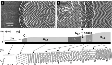
Hybrid structures, a combination of basic structures like parallel cylinders, perpendicular cylinders, perforated lamellar or wetting layers were observed when the film–interface interactions are dissimaler at the two interfaces30. Neck forming cylinders, for example, which is a combination of parallel and perpendicular cylinders was observed38. Also, perforated lamellas, where one of the block is in a lamellar structure, whereas the other is cylindrical, has been observed for asymmetric BCPs20.
Depending on the layer thickness, cylinder orientations can be perpendicular or parallel, similar to lamellar BCP behavior30. Terrace formation with different layer thicknesses and thus different cylinder orientations are also observed. The parallel orientation is supposed to be preferred due to the energy gain of the two degrees of freedom compared to one in perpendicular orientation39. Then, only in very thin films, where the bulk morphology would be too much distorted, a perpendicular orientation would be thermodynamically preferred. When the layer thickness is about t = (n-1/2)L0, the layer ruptures and forms terraces with different heights with integer step heights, leading to the formation of different morphologies and orienations39,40. An example of terrace formation and corresponding simulations of a symmetric polystyrene–polybutadiene triblock BCP (PS-b-PB-b-PS) are shown in Figure 1-13 (note that ABA triblocks show similar thermodynamic behavior as AB diblock copolymers41)40.
Figure 1-13: (a,b) Scanning force microscopy (SFM) phase images of thin films of PS-b-PB-b-PS on Si substrates after annealing in chloroform vapor. PB wets the substrate and bright areas corresponds to PS microdomains. (c) Schematic height profile of the phase images shown in (a,b). (d) Simulation of an ABA block copolymer film with increasing film
thickness. B shows preferential wetting towards the surface39.
In conclusion, the interplay of the strength of the surface energy of the confining interfaces (substrate and air) and the thickness of the layer, thus the deformability of the bulk structure, defines the arrangement of the microdomains.
16 1.3.2.c Manipulation of Interfacial Interactions
Over the decades, significant effort have been devoted to controlling the orientation of microdomains, especially for lamellas. Horizontal orientation of lamellae is undesirable in lithography applications, because their structure cannot be transferred into the substrate. The orientation of cylinders, on the other hand can be either horizontal (for semiconductor fins) or vertical (for contact holes) orientation. In order to overcome preferential interactions, several strategies have been presented. Note, that the manipulation of interface interactions becomes even more challenging when the χ-interaction parameter is high due to the high difference in interfacial energies of the blocks. However, for lithography applications, high-χ BCP are desired as they allow for lower molecular weights, so smaller feature sizes.
The most simple method to tune interfacial interactions is probably the grafting of polymer brushes onto the substrate, which was first presented in 1997, by Mansky et al.42. An end-functionalized random copolymer of Polystyrene – random – Poly(methyl methacrylate) (PS-r-PMMA) was grafted onto a substrate. When a block copolymer is deposited onto this brush layer, precise control over the orientation could be obtained by varying the composition of the random copolymer brush43. When precisely controlled, random copolymer brushes enable the neutral wetting of lamellar BCPs and thus the perpendicular orientation of the lamellae. In a similar way homopolymers can be grafted onto substrates in order to trigger the preferential wetting of just one block in asymmetric BCPs. In cylindrical BCPs for example, this enables the horizontal orientation of cylinders33,44. A variation of the grafting procedure is the integration of cross-linkable units into the BCP. Drockenmuller and coworkers demonstrated the neutral wetting of PS-PMMA when the PS block was incorporated with cross-linkable benzocyclobutene, altering its surface tension45,46.
Substrate surface modification is not always possible or wanted. For brush grafting for example, the substrate has to be specifically altered in order to allow the grafting. For hydroxyl terminated brushes the surface has to be an oxide layer for instance. Sometimes, additional process steps have to be integrated in order to obtain an appropriate substrate surface. An alternative and or complementary effective method is using top-coats that can be deposited on the BCP in order to change the BCP/air interface interactions. Bates and coworkers employed maleic anhydride top-coats on high-χ Polystyrene-block-Polytrimethylsilylstyrene-block-Polystyrene and Polytrimethylsilylstyrene-block-Polylactide. When baked, the top-layer switches polarity, initiating the neutral wetting of the BCP.
Further sophisticated methods to modify the orientation of BCPs is the application of electrical fields47–49. Morkved and coworkes applied an electric field on cylindrical PS-b-PMMA and oriented the PMMA cylinders parallel to electric field lines exceeding 30kV/cm48. This phenomenon is due to the difference in the dielectric constant of the blocks and was further studied via quasi in-situ scanning force microscopy
17
imaging by Olszowka et al.49. Kathrein and coworkers combined the application of an electric field and a topographical guidance of PS-b-PDMS. The orientation of the cylinders was either parallel or perpendicular to the guiding templates depending on the electric field orientation47.
Surfaces with topographical structures could also induce a specific orientation to BCPs. Bai et al. were able to orient a lamellar PS-b-PDMS perpendicular to the surface within extremely high trenches, taking advantage of the preferential wetting at the vertical sidewalls of these high aspect ratio templates50.
Orientation and morphology control can also be obtained during solvent vapor annealing (SVA) which will be discussed more in detail later in the next section and in chapter 251–53. A solvent vapor can mediate the BCP/air surface energy and act as a neutral layer to both blocks. Thus perpendicularly orientation of lamellae or cylinders can be obtained without the use of neutral brush layers53,54.
1.3.2.d Microphase Separation via Annealing
In order to obtain a regular thin film of block copolymers, it is usually solvated in a solvent and then spin-coated onto the substrate. By adjusting the degree of dilution of BCP in the solvent and the spinning speed, the desired thickness can be precisely controlled. This rather simple step implicates already complex mechanisms that are important for the subsequent microphase separation and is schematically illustrated in Figure 1-14.
Figure 1-14: Schematic illustration of the spin-coating process55
Depending on the BCP and the solvent, either micellar or rod-coil structures are formed in solution (Figure 1-14B and C). When deposited onto the surface via spin-coating, the solvent evaporates quickly and the BCP is trapped in a disordered non-equilibrium state. Well organized morphologies over large areas are unlikely to be produced right after spin-coating. Block-to-block interactions are reduced due the entanglement of the polymer chains and the presence of residual solvent and trapped free volume (Figure 1-14E)55. The structure of the film depends on the temperature, spin speed and nature of the solvent (evaporation rate and selectivity). In selective solvents (the solvent favors the solvation of one block) the
18
BCP can form amphiphilic micelles that are then deposited into hemi-micelles on the substrate (Figure 1-14D)55. Under certain conditions, ordering of the micelles can be obtained right after spin56. For most applications, regular periodic arrays of structures are desired and hence, in the case where a disordered, metastable structure is obtained after spin-coating, an anneal process is required. The annealing allows an ordered arrangement of nanostructures and can eliminate defects. Kinetically trapped structures, obtained after spin-coating, are usually annealed thermally or by solvent vapor in order to gain enough energy and chain mobility to rearrange into ordered structures. Thermal annealing (TA) is the most simple method to obtain long range ordering as it is easy to be inserted into industrial processes, especially when it comes to up-scaling of the process. During this step, the BCP is typically heated above its glass transition temperature (Tg) but below its decomposition temperature in order to approach TODT and hold at elevated temperature for a certain amount of time. Then, the BCP is simply left at ambient temperature to cool down. The initial thickness of the film is here crucial and when not correctly chosen, thermal annealing can cause the rupture of the film with hole or island formation57,58. For high-χ BCP, the ODT is generally extremely high, and thus not approachable, mainly due to thermal degradation of the polymers at high temperatures51. Alternatively very long annealing times of tens of hour or days below the degradation temperature are possible, but not interesting for industrial applications.
Solvent vapor annealing (SVA) is an alternative way to introduce order in BCPs and has been introduced for high-χ BCPs, when the ODT is difficult to attain due to thermal degradation. In this process, the spin-coated BCP film is kept in a controlled atmosphere containing solvent vapors at temperatures usually well below the Tg. The solvent molecules swell the BCP and act like a plasticizer, thus lowering its Tg and enhancing the chain mobility at room temperature59. Upon evaporation of the solvent, the BCP forms well-organized nanostructures. Probably the first to present a sort of SVA were Kim and Libera who prepared solutions of polystyrene (PS)-polybutadiene (PB)-polystyrene (SBS) triblock copolymers in toluene and left them to dry at different evaporation rates54. The authors obtained well-arranged PS cylinders in a matrix of PB when the sample was exposed to the solvent for a long period of time. Other morphologies and orientations were obtained at different evaporation rates. SVA gained later in popularity after the work of Kim and coworkers that presented the annealing of polystyrene-block-polyethylene oxide (PS-b-PEO) in benzene vapors. Highly ordered hexagonally packed PEO microdomains with long range order were obtained in a PS matrix when the BCP was placed in a benzene saturated chamber at RT. Numerous parameters have an impact on the final nanostructures after SVA. As explained in the previous section, the solvent vapor can mediate surface energies at the BCP/air interface and can change the preferential wetting of the free surface. Also, the solvent can induce a screening effect in mediating the unfavorable interactions of the block, thus
19
affecting the effective χeff32. Selective solvents can selectively swell only one of the blocks, modifying the effective volume fraction and enabling the access to different morphologies, depending on the solvent51,60,61.
1.3.3 Large Area Orientation of BCPs
Once annealed on plane substrates, the BCP arranges with short-range lateral ordering in so called fingerprint orientation, when showing cylindrical or lamellar morphology and in mulitcrystalline domains for sphere morphology. Small grains of nanostructures, having all a different orientation are formed at the surface. For many applications like bit patterned media or lithography masks, however, periodic domains with a high degree of ordering are required. Controlling the orientation of BCP microdomains with artificial surface modifications (either topographically or chemically) is called the directed self-assembly (DSA) of block copolymers. The use of chemical patterns for orientation control is called chemoepitaxy whereas that of topographical structures is called graphoepitaxy.
1.3.3.a Chemoepitaxy
In chemoepitaxy, chemically modified patterns are used to guide the block copolymer self-assembly. In this technique, the patterns that are created at the surface of a substrate strongly interact with the BCP, and the size of the pattern (LS) is comparable to that of the BCP period (LS ≈ L0). When a BCP film is deposited on top of this pattern, it minimizes its free energy by minimizing the amount of dissimilar interactions and align perfectly with the underlying pattern62. The ideal geometry of the chemical pattern has LS ≈ L0. If the commensurability of the pattern derives from this spacing, the BCP stretches and compresses to a certain amount in order to fit the chemical prepattern62. It was shown on lamellar PS-b-PMMA that this mismatch between L0 and LS supports ±10% of the ideal LS before losing the ordering effect and arranging in a fingerprint orientation63. The Nealey group extensively worked on the chemoepitaxy of BCP and influenced the progress of this domain greatly64–67. In the Liu–Nealey resist trimming or University of Wisconsin (UW) flow62, a hydroxyl terminated PS monolayer is grafted onto a Si substrate68. A resist layer is then patterned and developed on top of this layer. Oxygen plasma treatment of the exposed PS layer led to polar, hydrophilic PS patterns. After resist-stripping, the surface is then alternately covered with hydrophilic and hydrophobic patterns. The deposition and annealing of PS-b-PMMA on these substrates leads to the perfect alignment of the microdomains over large areas. An extension of this works shows the successful alignment of PS-b-PMMA on complex structures with bends (45°, 90° and 135°) and segments, jogs and T-junctions (Figure 1-15)65,67.
20
Figure 1-15: Top view scanning electron microscopy (SEM) images of (a) angled lamellae of PS-b-PMMA65 and (b)
PS-b-PMMA directed to assemble into nested arrays of jogs, isolated PS-b-PMMA jogs, isolated PS jogs and arrays of T-junctions67
More interestingly for future lithography applications are also density multiplication structures. In this case sparse chemical patterns, where LS = nL0, are used to enhance the resolution of the initial pattern. PMMA patterns were found to be able to interpolate additional PMMA domains between guiding patterns, while maintaining its natural L0, when LS = 2L066,69. A schematic of this process is depicted in Figure 1-16
Figure 1-16: Schematic illustration of sparse chemoepitaxy. The chemical patterns have a pitch twice as highs as that of the block copolymers. The self-assembled block copolymer doubles the spatial frequency of the underlying guiding
chemical patterns69
1.3.3.b Graphoepitaxy
Graphoepitaxy uses structural reliefs to guide the self-assembly of BCP in thin films and enhances lateral ordering of the nanostructures. In contrary to chemoepitaxy, the general pattern size of the topographical structures are a few times larger than the intrinsic domain spacing of the BCP. The topographic patterns are obtained with one of the typical lithography methods presented previously in this chapter. One of the
21
drawbacks of graphoepitaxy compared to chemoepitaxy is that some of the surface area is lost, due to the guiding patterns. However the extreme density multiplication and ability to align the BCP into complex structures are key advantages.
The first applications of graphoepitaxy on BCP were reported by Segalman and coworkers in the early 2000s70–73. Spherical Polystyrene-b-Poly-2-vinylpyridine (PS-b-P2VP) microdomains were aligned within trenches and wells of different depth and width. Large area single crystal of spheres were obtained after thermal annealing when aligned in trenches (Figure 1-17a)70. The group found out that the two parameter depth and width of the guiding trenches are crucial for the alignment of the BCP. Good lateral ordering was only obtained when the depth was equal or greater than L0 and the width not greater than 185*L0 (5µm) 70. In parallel, the Ross group also thoroughly investigated the effect of graphoepitaxy on a different spherical BCP. Polystyrene-b-Polyferrocenyldimethylsilane (PS-b-PFS) were chosen because of the high etch selectivity of the iron containing PFS block, which can be used as a hard mask for pattern transfer into an underlying functional material74–78. Trench patterns of 80 nm depth and various widths that were a few times larger than the natural period of the BCP were tested. In that way, the number of PS-b-PFS rows inside the trenches was controlled (Figure 1-17b). An integer number N of rows of spherical microdomains was found when the width (W) of the trenches was (N-0.5)L0 < W > (N+0.5)L0. When the width of the trenches was not commensurate with the period of the BCP (W≠nL0), the spheres were compressed or extended in order to accommodate the trench width.
Figure 1-17: a) top view SFM image of a single crystal of PS-b-P2VP on top of a mesa69. b) Top view SEM images of aligned
PS-b-PFS spheres in trenches of various widths (N=2-12 rows)75
Furthermore, they found out that the defect formation can be induced into the microdomain array when defects in the guiding feature were present79.
The Ross group extended their work on graphoepitaxy with a cylindrical Polystyrene-b-Polydimethylsiloxane (PS-b-PDMS) system33,80,81. PDMS shows comparable high etch selectively as PFS, because of its high amount of silicon in the backbone. The PS block can be easily etched away while the
22
PDMS block transforms into a robust hard mask material. PS-b-PDMS is therefore interesting for pattern transfer. Additionally PS-b-PDMS has a high incompatibility (χ≈0.26 at RT82,83) and thus smaller N values, which are related to L0, can be used. However, due to their high surface tension difference, special attention has to be paid to the interface interactions when confined in lateral template patterns. Jung and Ross confined cylindrical PS-b-PDMS microdomains in PDMS-brush coated trenches, in order to obtain vertical orientation of the PDMS cylinders33. They obtained selective orientation of cylinders by varying simultaneously the mesa width and solvent annealing parameters. Later, concentric ring patterns with the same BCP system were obtained by the Ross group80. By playing with the pattern diameter, the organization of the concentric ring formation could be controlled. Other interesting structures like rectangular, triangles and circles have been used for cylindrical PS-b-P2VP guiding by Chai et al84 (Figure 1-18b). After alignment of P2VP cylinders inside the templates, the cylinders were loaded with metal ions in order to obtain metal wires after polymer etch.
Figure 1-18: top view SEM images of (a) PS-b-PDMS cylinders in concentric ring patterns with varying diameters79 and (b)
Platinum nanowires obtained from self-assembly of PS-b-P2VP in different shaped templates. The different orientations
of the cylinders in c) and d) are due to a defect in the template structure81.
For lamellar systems, the interactions of walls and BCP and the commensurability of the templates govern the orientation and size of the microdomains. Park and coworkers investigated the behavior of lamellar PS-b-PMMA domains in trenches of different surface energies85. For perpendicular orientation of the lamellas, it is necessary that the bottom surface of the trenches is neutral for both blocks while the feature sidewalls has to interact selectively to either PS or PMMA. When all sidewalls and bottom surface showed preferential wetting with the PMMA block, the lamellae aligned parallel to the substrate. A neutral brush layer on sidewalls and bottom layer led to perpendicular arrangement but without long range arrangement
23
of the microdomains. In this case, a precise control of layer thickness, molecular weight and commensurability is important to obtain long range ordering85.
1.3.4 Application of Directed Self-Assembly in Nanomanufacturing
Recently, the ITRS introduced DSA as a new potential complementary lithography technique for next-generation microelectronic manufacturing86. DSA has this great potential due to its ability to create high-throughput, low-cost and high resolution nanopatterns. Several groups have thus investigated the potential of DSA in real applications.
Bit patterned media are hard disk drive technologies that store data in magnetic islands, in which one island contains only one bit. Conventional hard disk drives store data in grains of continuous thin films, where one bit of data consists of around 20 grains. In the attempt to increase storage density and reduce the bit size, thermal stability and media noise problems were caused, that could be solved by using bit patterned media. The magnetic data is here stored in lithographically defined single domain islands, with high area density of 1Tdot/in2 and beyond62. This is where DSA can be interesting by creating large area, high density templates for pattern transfer87. Several reports show the directed self-assembly with chemical patterns of large PS-b-PMMA microdomains that are created and transferred into Si substrates. After pattern transfer these templates can serve as a master for nanoimprinting to create disks with magnetic media88,89. An example of this process is presented in Figure 1-19
Figure 1-19: top view and tilted SEM images at different stages of the bit patterend media fabrication. (a) BCP template after PMMA removal, (b) Si master template after reactive ion etching, (c) Magnetic islands, (d) Bright field transmission
24
Other reports show the DSA of spherical and cylindrical PS-b-PDMS by graphoepitaxy90,91. Guiding patterns were designed to be up to three times as large as the natural period of the PS-b-PDMS. The PS-b-PDMS feature size was down to 6 nm small. By using 2D dots array or 1D groove prepatterns different geometries have been obtained (Figure 1-20). The obtained CoCrPt alloy dots have been demonstrated with highest density of 1.5Tdot/in2 for a guided media.
Figure 1-20: (a) Schematic representation of directed self-assembly of sphere-forming PS-b-PDMS thin films by a 2D
low-topographic holes array resist prepattern with LS=2L0 and corresponding SEM top view images. (b) Schematic
representation of directed self-assembly of sphere-forming PS-b-PDMS thin films by a 1D high- topographic groove
pattern and corresponding SEM images (top L0=22.3 nm, bottom L0=15.2 nm)87
Fin field-effect transistors (finFET) are another possible application of DSA of BCPs. FinFETs are 3 dimensional double gate transistors that are traditionally build on Silicon on Insulator (SOI) substrates. FinFETs use a conducting channel that stands on the insulator material, shaped like a fin. This fin-shaped gate electrode allows the connection of multiple gates on one single transistor. The implementation of periodic line-shaped BCP patterns could reduce their feature size and improve the performance. By customizing the guiding pattern for graphoepitaxy, Tsai et al. demonstrated the fabrication of a 29 nm pitch finFET device, derived from the DSA of PS-b-PMMA92. The authors present the formation of self-aligned pattern-free regions between groups of aligned lines and a cutting of lines by additional lithography and etching processes. The process flow of the finFET fabrication is depicted in Figure 1-21
25
Figure 1-21: (a) Schematic illustration of the process flow for forming groups of silicon on insulator (SOI) fins with PS-b-PMMA templates with a controlled fin spacing. Tone inversion operation is applied after the DSA pattern is transferred into the underlying layer. The tone inverted image is then transferred into a fin hard mask layer and 20nm of SOI. (b) Top view SEM image of a group of fins obtained after the process shown in (a). (c) TEM cross-section image of obtained 29 nm
pitch SOI fins89
Finally, the translation form laboratory scale DSA samples to industrial scale full 300mm wafers is important to understand mechanisms on a large scale and evaluate if processing steps are adapted for industry. The Liu-Nealey process has been implemented on a 300mm wafer production line93. PS-b-PMMA with a pitch of L0=25 nm were aligned via chemoepitaxy on the wafer. This gives a new basis to study BCP behavior on large surfaces and especially defect origins and propagation.
1.3.5 High-χ Block Copolymers
The most studied system of BCP is PS-b-PMMA due to its easy synthesis and familiarity of the microelectronics industry with the two homopolymers PS and PMMA. However, PS-b-PMMA has a relatively low χ-value of 0.0494. As explained above, the χ has great impact on the phase separation. The higher the compatibility or the lower the χ parameter the less defined are the microdomains after phase separation. On the contrary when the χ parameter is high and the degree of polymerization, N, is small, the domain spacing of the system can reach its smallest values. In order to phase separate, we have seen that the BCP has to have a χN value of at least . . Taking into account the low value of PS-b-PMMA of 0.04, the polymerization N has to be at least 250 in order to obtain microphase separation. The lowest obtainable period for PS-b-PMMA is hence of about 20 nm. This is why high-χ systems have been introduced. Using BCPs with a higher χ allows to use lower N polymers and thus give access to smaller domain sizes. Numerous BCP with high χ parameter have been reported in the last decade. The incompatibility between