The Design of Low-Power Digital Datapath
Circuits
by
Jeffrey L. Steinheider
Submitted to the Department of Electrical Engineering and Computer
Science
in partial fulfillment of the requirements for the degree of
Master of Engineering in Electrical Engineering and Computer Science
at the
MASSACHUSETTS INSTITUTE OF TECHNOLOGY
June 2000
@
Jeffrey L. Steinheider, MM. All rights reserved.
The author hereby grants to MIT permission to reproduce and
distribute publicly paper and electronic copies of this thesis document
in whole or in part.
ENG
Author .
.... t.m.n.t.o.. f.. .. t... ..Department of Electrical E neering
and Computer Science
May 19, 2000
Certified by ...
...
Anantha Chandrakasan
Associate Professor
ThpsisSipervisor
Accepted by...
Arthur C. Smith
Chairman, Department Committee on Graduate Theses
MASSACHUSETTS INSTITUTE OF TECHNOLOGY
JUL
27 2000
The Design of Low-Power Digital Datapath Circuits
by
Jeffrey L. Steinheider
Submitted to the Department of Electrical Engineering and Computer Science on May 19, 2000, in partial fulfillment of the
requirements for the degree of
Master of Engineering in Electrical Engineering and Computer Science
Abstract
This thesis outlines the design of the digital section of a transmit DAC, as well as the methods used for limiting the power consumption of the design. The methods emphasized are ones that provide noticeable reduction of the power, and can be used again without adding to the development time of later designs. This thesis describes the use of dynamic flip-flops and different architectures of FIR filters as two methods that yielded the best savings in power consumption.
Thesis Supervisor: Anantha Chandrakasan Title: Associate Professor
Acknowledgments
I would like to thank all of my family and friends; without their continuing
encour-agement and support none of this would have been possible. Liz, Jan, Mom and Dad, you've all helped me through the hard times and kept me going. Thanks to all of the employees at Analog Devices in the High Speed Converter Group for everything they have taught me during my last three years there. Special thanks to Donald Paterson and Steve Harston for their assistance with this thesis. Finally I would like to thank my thesis supervisor Anantha Chandrakasan for his guidance and patience.
Contents
1 Introduction 8
1.1 Motivation for Low-Power Digital Circuits . . . . 9
1.2 Sources of Power Consumption . . . . 10
1.2.1 Static Power . . . . 10
1.2.2 Dynamic Power . . . . 11
1.3 Methods for Power Reduction . . . . 12
1.3.1 Voltage Reduction . . . . 12
1.3.2 Reduction of the Switching Activity . . . . 12
1.3.3 Reduction of the Load Capacitance . . . . 13
1.3.4 Low Power Processes . . . . 13
1.4 Organization . . . . 14
2 The Design 15 2.1 SP I P ort . . . . 15
2.2 Built in Self Test . . . . 17
2.3 The Clock Divider . . . . 18
2.4 The Digital Datapath . . . . 18
2.4.1 Data Formatter . . . . 19
3.2 TSPC Dynamic Flip-Flop ... 27
3.3 Evaluation of the Flip-Flop Designs . . . . 29
4 FIR Filter Architectures 32 4.1 Multiply-Accumulate Architecture . . . . 32
4.2 Transposed Form Architecture . . . . 33
4.3 Direct Form Architecture . . . . 33
4.4 Reducing Multiplies. . . . . 34 4.5 Polyphase Implementation . . . . 35 4.6 Im plem entation . . . . 37 4.7 Verification . . . . 38 4.7.1 Code Verification . . . . 38 4.7.2 Timing Verification . . . . 39 4.7.3 Power Verification . . . . 40 5 Conclusion 41 A Verilog and Module Compiler Code 43 A.1 Stage 1 Module Compiler Code . . . . 43
A.2 Stage 2 Module Compiler Code . . . . 44
A.3 Stage 3 Module Compiler Code . . . . 45
A.4 BIST Pseudo-Random Number Generator Verilog Code . . . . 46
A.5 BIST Signature Verilog Code . . . . 47
A.6 DC Test Bench . . . . 50
A.7 Behavioral Versus Gate Level Test Bench . . . . 51
A.8 Behavioral Model of the Stage 1 FIR Filter . . . . 53
List of Figures
2-1 Block Diagram of the Design . . . .
2-2 An LFSR Pseudo-random Number Generator . . . .
2-3 2-4 2-5 2-6 2-7 3-1 3-2 3-3 3-4
The Digital Datapath . . . . Frequency Response of Filters Providing a 2X Frequency Response of Filters Providing a 4X Frequency Response of Filters Providing a 8X Advantages of Hilbert Transform . . . . Standard Cell Transmission Gate Flip-Flop . . 9T Dynamic Flip-Flop . . . . Final 9T Dynamic Flip-Flop Design . . . .
TSPC Dynamic Flip-Flop . . . . Rate of Rate of Rate of Interpolation Interpolation Interpolation
4-1 Multiply-Accumulate Form of an FIR Filter . . . . 4-2 Transposed Form of an FIR Filter . . . . 4-3 Direct Form of an FIR Filter . . . . 4-4 Reusing Multipliers in the Direct Form of an FIR Filter . 4-5 Noble Identity . . . . 4-6 Polyphase Filter Implementation . . . .
16 17 19 20 21 22 23 . . . . 25 . . . . 26 . . . . 28 . . . . 29 33 34 34 35 36 37
List of Tables
3.1 Flip-flops in the design . . . . 24
3.2 Flip-flops in the design . . . . 25
3.3 Transmission Gate Flip-flop Timing Statistics . . . . 30
3.4 9T Flip-flop Timing Statistics . . . . 30
3.5 Flip-flop Power Statistics . . . . 31
4.1 Timing Simulations with Pathmill . . . . 40
Chapter 1
Introduction
Power consumption has become an increasingly important consideration in the design of digital circuits. Techniques must be developed to reduce the power consumed in high performance digital datapaths to keep pace with the increasing complexity and size of digital designs. Many papers have been written on determining the sources of power dissipation in digital circuits, and reducing the power consumption, but much of this prior work has been focused on methods that apply to the design of processors. This thesis will cover the design of the digital section of an Analog Devices TxDAC. The TxDAC is a DAC designed for the transmission path of broadband and multi-carrier signals. The TxDAC features on-chip digital interpolation filters that eliminate the nearby signal images, and enhance the DAC's inband dynamic range. The inter-polation filters for this design are hard-coded with variable interinter-polation rates of two, four and eight times. The interpolation filter will receive a majority of the treatment, because it performs the bulk of the processing and consumes the most power in the design.
Special attention will be given to the methods which helped to reduce the power consumption of this design while keeping with the design methodology that is used at Analog Devices. This will make it possible to reduce the power consumption of
1.1
Motivation for Low-Power Digital Circuits
As more signal processing has been incorporated into the digital domain, the number of transistors and the power consumption in digital designs have increased dramati-cally. This causes several different problems.
Perhaps the most obvious problem occurs in portable systems. The more power a system consumes, the shorter its battery life will be. Portable systems that consume too much power require more expensive, specialized batteries, or the device will run for a shorter amount of time. The number of transistors that can be fit onto a single chip has doubled every two years, while the capacity of a AA battery doubled only over a 10 year span from 1982 to 1992 [11]. Since the improvements in batteries have not even come close to matching the increase in the number of transistors that can be fit onto a chip, clearly the problem rests with digital designers to ensure that the power consumption of their designs does not rise along with the complexity.
The amount of power dissipated in a chip dictates the amount of heat that the chip creates. For IC manufacturers, chips with high power consumption require more heat tolerant materials for the packages that can quickly dissipate excess heat into the surrounding air. These materials are more expensive, making integrated circuits more expensive to manufacture and reducing profit margins. The excess heat also cre-ates problems for system designers, who must use better and more expensive cooling systems to ensure that their designs don't overheat.
In addition to limiting battery life and causing overheating, excess power con-sumption also reduces the reliability of integrated circuits. The increase in current heightens the possibility of metal migration in the wires, which eventually leads to breaks in the wires.
In the area of mixed signal design, the power consumed by digital circuits affects the noise performance of the analog circuitry. The digital circuitry is resistively coupled through the substrate, and the digital section will create more noise in the analog circuitry with increasing power consumption.
consumption of competing chips can often be the deciding factor of being included in a system. Since area has become less of a concern with the continually shrinking process sizes, integrated circuit manufacturers have more reasons now than ever before to work towards lowering the power consumption of their designs.
1.2
Sources of Power Consumption
In digital CMOS circuits, the average power consumption is often divided into two categories, static power and dynamic power
[21.
Pavg = Pstatic + Pdynamic (1.1)
1.2.1
Static Power
In CMOS circuits the static power is caused by subthreshold current and reverse biasing. The subthreshold current is shown in Equation 1.2 and the current from reverse biasing is shown in Equation 1.3.
W14 2 (VGS -VTH)
ISUB =- A -COX ( e VT (1.2)
V
ID = IS(eW - 1) (1-3)
I is the reverse saturation current, V is the voltage from the drain to the bulk,
Mo is the carrier surface mobility, Cox is the gate oxide capacitance per unit area, W and L are the effective width and length of the device, and VT is the thermal voltage
[3}. The leakage current typically accounts for very little of the total average power,
and it is usually dependent on the process. For these reasons it will be ignored in this thesis.
1.2.2
Dynamic Power
The dynamic power is frequently divided into two components, the short circuit power and the switching power.
Pdynamic Pswitching ± Pshort-circuit (1.4)
The short-circuit power is the result of a direct path from power to ground that will exist for a period of time when both the nmos and pmos transistors are on at the same time. The key to reducing the amount of short-circuit power is to ensure that the input and output transitions of the circuit take an equal amount of time [16].
The most important component of the dynamic and even of the total average power is the switching power. The equation for the switching power of a CMOS circuit is shown below.
Pswitching = Cf-f * CL * Vdd V (1-5)
In the equation, CL is the total load capacitance that the circuit is driving.
f
is the frequency of the clock, and a is the probability that the node will transition to a different state in one clock period. The Vdd term is the voltage of the power node, while V is the voltage swing of the input node. For most standard CMOS circuits the voltage swing of the input node is equal to the voltage of the power node, creating the term Vd. However, there are some circuit styles in which the voltage swing is smaller than the power voltage.Typically, the switching power is the most dominant factor in the average power, accounting for around 90% of the total average power in a well-designed circuit. For these reasons, the effort of this thesis will be to reduce the dynamic power of digital
CMOS circuits since this will lead to the greatest reduction in the overall power.
From this equation, it can be seen that there are several possibilities for reducing the power consumed in a digital circuit. Power reductions can be achieved by reducing the switching frequency, the clock frequency, the capacitance, or the voltage of the circuit.
1.3
Methods for Power Reduction
1.3.1
Voltage Reduction
The technique that provides the greatest benefit is to reduce the voltage driving the circuit, because the switching power is dependent on the voltage squared. Reducing the voltage slows down the circuit, as shown in Equation 1.6 [12].
(CLVDD k( 1V) 2 1 1 VTP1 2 (1.6)
2 kn(VDD - VTn2 kp(VDD - p2
The circuit can be pipelined or implemented in parallel so that the driving voltage can be lowered without sacrificing the overall performance of the circuit. Although implementing a circuit in parallel doubles the capacitance C, the dependence of the switching power on the square of the voltage from equation 1.5 will make up for the doubling of C and result in a net reduction of power consumption. Other techniques have been developed to lower the voltage on large buses that exist in large designs
[7]. For the purposes of datapath circuits such as the one presented here, this is not
a viable option because the data flows from one processing element to another, and there are no buses that traverse the entire design.
1.3.2
Reduction of the Switching Activity
Another method for reducing power consumption is to try to reduce the level of switching activity that occurs in the circuit. This can be applied to two parts of the circuit. An effort can be made to reduce spurious transitions that occur between flip-flops, and the clock can be gated to reduce the frequency with which the flip-flops switch.
Reducing the number of spurious transitions requires the careful balancing of delay paths, so that any changes in data arrive at each cell at the same time, ensuring that
Clocks can be gated in several ways. The clock can be gated individually to each flip-flop with logic that will prevent the clock pulse from reaching the flip-flop if the incoming data matches the previous data [6]. This is supposed to reduce the loading on the clock net, but it does increase the complexity and area of the circuitry.
A second method for gating the clock is to gate it before it reaches large sections
of the design that may not be in use all of the time. Since this design is for a standard product with many features, not all of these features will be useful to all users. Using gated clocks to turn off the sections that are not in use can save a significant amount of power. In addition there are several built-in test circuits that will never be used outside of the test floor, and the clock should always be turned off to these sections when the chip is in normal operation.
1.3.3
Reduction of the Load Capacitance
As seen from Equation 1.5, reducing CL will also reduce the dynamic power in a circuit. One of the best methods for reducing the load capacitance of a design is to reduce the number of computations performed through the choice of the architecture and algorithm used for the specific task [4]. In this design, the architecture chosen for the FIR filter plays an important role in achieving the power consumption goals. The FIR filters also use as much rounding as possible to keep the datapath width to
a minimum, and all constant multiplications are implemented as shifts and adds.
1.3.4
Low Power Processes
Several processes are currently being developed that show promise in reducing the power of CMOS circuits. One of these processes is Silicon on Insulator (SOI). SOI offers better power efficiency because it permits lower threshold voltages to be used, which in turn allows for lower supply voltages. It also eliminates much of the source and drain junction capacitance, which leads to higher switching speeds in addition to power savings [8].
processes because the design for this project is scheduled for production in several months. A new process needs to be tested for reliability and would require a new analog design for the DAC, which was not feasible for this project.
1.4
Organization
This chapter covers some of the motivations for lowering the power consumption of digital circuits, as well as mentioning some of the techniques that have been employed
in the past to save power.
Chapter two describes the overall design of the DAC's digital section and the requirements and function of each of the subsections of the design.
Chapter three covers the use of dynamic flip-flops to improve the power consump-tion of the design.
The fourth chapter describes the architectural optimizations that can be made to save power in the design of digital FIR interpolation filters. It also details the implementation and testing of the interpolation filters designed in this chip.
Chapter 2
The Design
The design is for a configurable interpolation filter that will interpolate the data to two DAC's by a factor of two, four, or eight times. There is also a modulator function that performs a Hilbert transform modulation to either 1 or 1 of the final sampling frequency of the two DAC's. The DAC has 16 bit precision, so the filters must have at least 16 bit data. The DAC is designed to operate at a top speed of 400 MSPS, so in each of the different interpolation modes, the filters must be able to output data
at a rate of 400 MSPS. A block diagram of the design is shown in Figure 2-1.
The digital section of the design can be divided into four sections: the datapath, the Built in Self Test (BIST), the clock divider, and the SPI port. The digital datapath is the largest section, consumes the most power, and will be the focus of this thesis.
The other three sections are mentioned here for completeness.
2.1
SPI Port
The SPI port is a serial port interface to allow embedded processors to communicate with the chip. There are many setup options that can be set for the chip, and the SPI port allows all of these options to be programmed without requiring a large number of pins. The SPI port controls the operation of the interpolation filters, allowing users to choose the amount of interpolation to perform, and it also controls the BIST. The
Figure 2-1: Block Diagram of the Design
I
____I
___Clock Divider
High Speed Clock from PLL Data
Data
BIST
SPI Data SIPr
Digital Datapath
SDAC
Figure 2-2: An LFSR Pseudo-random Number Generator
A 4 4
CLK
the SPI clock from coupling with the signal noise, but this will also lower the power of the SPI section during full operation. The SPI port design is a modified version of the SPI port from an earlier Analog Devices Chip.
2.2
Built in Self Test
The Built in Self Test (BIST) is comprised of two parts. The first half of the BIST is a pseudo-random number generator that creates a sequence that does not repeat for 217 samples, and covers all possible binary values for a 16 bit number. This sequence is used as an input to the digital datapath, so that high speed data does not have to be driven on the pins of the chip during test. The pseudo-random number generator will always produce the same sequence, provided that it is initialized to the same value. The pseudo-random number generator is implemented using a linear feedback shift register (LFSR) [5]. A simple example of a 3 bit pseudo-random number generator implemented with an LFSR is shown in Figure 2-2.
The second half of the BIST is a signature module that computes a checksum of the output of the digital datapath, again using a LFSR. The signature module computes the checksum over a certain number of values. The checksum that is computed is then stored in registers of the SPI module, so that the checksum can be read through the SPI port. Both the signature module and pseudo-random number generator are
designs from previous chips.
These two subsections of the BIST can be used to compare the actual performance of the digital design to computer simulations of the design. The pseudo-random number generator will produce the same sequence in the computer simulation and the finished silicon. The signature module will produce the same output for each, as long as it has the same input data, and runs for the same amount of time. Differences between computer simulations and recorded data from the BIST for the silicon, or differences between different runs on the silicon, point to an error with the silicon.
2.3
The Clock Divider
The clock divider is necessary to create the multiple clocks needed for the datapath because of the different rates of interpolation. The clock divider divides down the high speed clock from the phase locked loop, which dictates the DAC's speed. Using the values set in the SPI port registers, the clock divider will then create the , 2' 4'1
and
}
speed clocks as they are needed. The rising edge of each slower clock is lined up with a falling edge of the faster clock, to ensure that no data race occurs when data is handed off between two clock domains.2.4
The Digital Datapath
The digital datapath is responsible for formatting the data as it arrives on the chip, performing the necessary interpolation and filtering, and then modulating the data using the Hilbert transform to either
}
or 1 of the output frequency. After passing through the modulator, the data must be decoded before it arrives at the DAC and is converted into an analog waveform. Figure 2-3 shows the block diagram describing the digital datapath.Figure 2-3: The Digital Datapath
FIR FIR FIR
Data -+Filter 1 -- o Filter 2 -- oo Filter 3 4 yThermometer +p DAC
Formatter Encoder
Hilbert Modulator
FIR FIR FIR
Data _yFilter 1 Filter 2 .. ,Filter 37- Thermometer +4 DAC
Formatter Encoder
2.4.1 Data Formatter
The data formatter is a very simple module that is in place to allow the data to be sent to the chip in either unsigned binary, or in two's complement format. All of the data on the chip is represented in two's complement form, so this module either converts unsigned binary to two's complement, or simply lets the two's complement data pass through to the rest of the datapath. Converting between two's complement and unsigned format is accomplished by inverting the most significant bit of the data.
2.4.2
Interpolation Filters
The interpolation filters will provide interpolation by a factor of two, four, or eight. There is also an option to bypass all of the interpolation filters to allow the data to travel straight to the DAC with no interpolation. To allow for multiple interpolation
rates, the interpolation filters are implemented as three half-band filters that provide a fixed rate of interpolation by a factor of two. In order to provide the lower factors of interpolation, the later filters can be bypassed. The clocks are gated to each filter so that when the data is bypassing the filter, the clock to that filter is gated off to reduce the power consumption of the inactive filter.
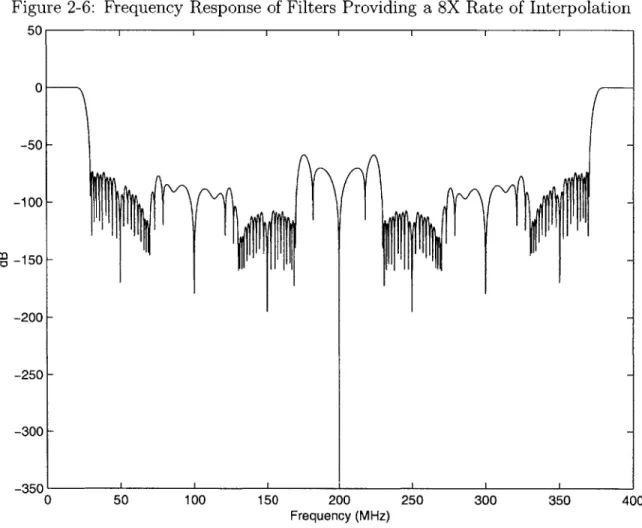
The filters are designed so that when they are providing a two or four factor of interpolation, the images are attenuated by at least 73 dB. For interpolation by a factor of eight, the farthest images are only attenuated by 45 dB. The lower require-ments for the higher factor of interpolation exist because the sin(x)/x rolloff of the
Figure 2-4: Frequency Response of Filters Providing a 2X Rate of Interpolation 5 0 I I I I I I I i I 0 -50 -100 -150 -200 -2501 0 10 20 30 40 50 Frequency (MHz) 60 70 80 90
DAC further attenuates the image, and at the eight times interpolation, the baseband
image and the first image are far enough away to allow for filtering in the analog do-main without too much trouble. The frequency response for the filters in the three interpolation modes are shown in Figures 2-4, 2-5, and 2-6.
2.4.3
Hilbert Modulator
The Hilbert modulator provides the option of modulating the data up to either - or8 of output sampling frequency of the DAC. Using the Hilbert modulator cancels out
to
0
-300 I I I I I I I I I
Figure 2-5: Frequency Response of Filters
20 40 60 80 100
Frequency (MHz
Providing a 4X Rate of Interpolation
120 140 160 180 200 50 0 -50* -100--150 I I I I I I I I I I I I I I I I I -200 -250 -300 -350 0
-Figure 2-6: Frequency Response of Filters Providing a 8X Rate of Interpolation 0 50 100 150 200 Frequency (MHz) 250 300 350 400 -50 -100 -150 -200 -250 -300 -350 0 I I I I I 5
Figure 2-7: Advantages of Hilbert Transform Modulation without using the Hilbert Transform Modulator
- -I
950 1000 1050
Modulation using the Hilbert Transform Modulator
950 1000 1050
Frequency (MHz)
Figure 2-7 shows the benefits of using a Hilbert transform to perform the modu-lation. In the figure, the final carrier frequency that is multiplied with the data has a frequency of 1 GHz. The data was output from the DAC at 400 MSPS, and was modulated to 100 MHz using the Hilbert transform modulator. The first window shows the resulting frequency band without the Hilbert transform modulator, while the second window shows the resulting frequency band using the Hilbert transform modulator.
After the Hilbert modulator, the data proceeds to the DAC, where it is decoded and then changed to an analog waveform.
0 -50 m 00 -IOU 800 850 900 1100 1150 Ca 0 -50 100 -150 800 00 00 850 900 1100 1150 12 .1 0 12
-Mil-Chapter 3
Low-Power Dynamic Flip-Flops
In the present design, and in other high performance designs, flip-flops are used heavily in order to pipeline the design. Pipelining is often necessary to allow the circuit to meet its performance requirements. Most digital filters require registers to hold state variables, so flip-flop cells frequently account for a majority of the area and they are among the most frequently used cells. Table 3.1 shows the number of flip-flops and total number of cells in the three FIR filters. Table 3.2 shows the percentage of cells and area that the flip-flops make up in the first two FIR filters.
All of the registers in the design were almost exclusively implemented using two
standard cells: a single output flip-flop and a negated single output flip-flop. Improve-ments to the power consumption of these two cells have the possibility of noticeably improving the power consumption of the entire circuit. This is especially true con-sidering that these cells also have the highest signal activity, since the clock changes its state twice every clock period.
Table 3.1: Flip-flops in the design Design Number of Total Number Module Flip-Flops of Cells
Table 3.2: Flip-flops in the design
Design Flip-Flops as Flip-Flops as Module Percentage Percentage
of Cells of Area Stage 1 FIR filter 35% 43% Stage 2 FIR filter 46% 56%
Stage 3 FIR filter 48% 62%
Figure 3-1: Standard Cell Transmission Gate Flip-Flop
The current flip-flops that are in the standard cell library are based on the classic transmission gate design, and are shown in Figure 3-1. The advantage of this design is that it is very robust, and also allows the clock signal to be held in a constant state for a long period of time. This facilitates creating a low-power standby mode. In the low-power standby mode, the clock is held constant, which effectively eliminates all of the dynamic power dissipation. However, these flip-flops are rather large (22 transistors) and their power performance can be improved.
Many other designs for flip-flops exist, including dynamic and adiabatic logic de-signs [1]. Several flip-flop dede-signs were avoided because they require two clocks that have a specific phase relation. It would be difficult to ensure that this phase relation was maintained throughout the chip in a high performance design, and routing two high speed clocks throughout the chip will also significantly increase power
consump-tion. The dynamic flip-flops, however, use only a true single phase clock, increasing
reliability and making it easier to route the clock net. Dynamic designs were cho-sen because in addition to their low-power properties, they also use considerably less
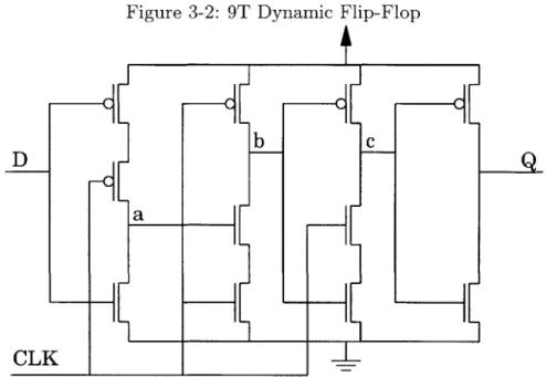
Figure 3-2: 9T Dynamic Flip-Flop
b
CLK
area and can operate at higher clock rates [17]. This makes dynamic flip-flops ideal candidates for the current design with its performance requirements. Two dynamic
flip-flops designs were considered, the 9T dynamic flip-flop, and the TSPC dynamic flip-flop.
3.1
9T Dynamic Flip-Flop
The original design for the 9T dynamic flip-flop is shown in Figure 3-2 as it was presented in [14] and also in [123. The design has this name due to the fact that in its original configuration, it contains only 9 transistors.
All three of the internal nodes in the flip-flop can be dynamic, depending on the state of the data. Node b precharges high while the clock is low. The precharging node
is not necessarily ideal for a low power application. It increases the power consumption of the flip-flop when the D is held at a logic zero state, which causes a logic zero to be
Several standard modifications were made to this flip-flop in order to make it more robust and to allow it to work in the current design. The original version of the 9T
flip-flop was for a single output inverting flip-flop. For the non-inverting flip-flop an inverter was added at the output, and for the new inverting flip-flop a buffer was added to the output. This was done in order to make sure that the flip-flop could drive higher capacitive loads, and also to ensure that a dynamic node is not driving the cell output. The cell output could contain a heavy capacitive load due to wire interconnect capacitance, or a large fanout into several cells.
Also, there is a disadvantage to the dynamic nodes when the standby mode is used and the clock is held at a constant state. If the clock is held low, then node c does not have an open path to either power or ground. Because of this, charge can slowly leak from the node, causing the voltage of the node to reside somewhere between power and ground. This would partially turn on both transistors in the following buffer, creating a straight path from power to ground. This resulting "crowbar" current can dissipate a considerable amount of power if this is allowed to occur, effectively ruining the low power standby mode.
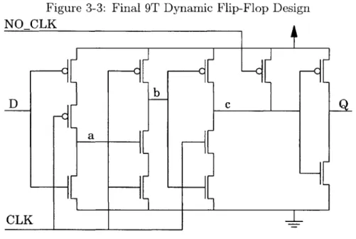
In order to avoid this, another pmos transistor is used to connect node c to the power rail, and a no-clk signal will be routed to this cell. The no-clk signal will be high in normal operation, and will be forced low when the clocks have been stopped during the standby mode. This transistor will force node c to a logic one, and remove the risk of developing crowbar currents in the standby mode. Because this transistor is not in the timing path, and crowbar currents take a long time to develop, the transistor can be the minimum size. The final non-inverting 9T flip-flop design is shown in Figure 3-3. Adding the no-clk signal to the flip-flop will add overhead to the design since it will be necessary to route this signal to every flip-flop in the design.
3.2
TSPC Dynamic Flip-Flop
The TSPC flip-flop earns its name from the fact that it requires only a true single phase clock. The TSPC flip-flop is slightly larger than the 9T design, in its original
Figure 3-3: Final 9T Dynamic Flip-Flop Design NO CLK b D c a CLK
form it has 12 transistors. The original TSPC design is shown in Figure 3-4.
All of the internal nodes in the original design are dynamic, however, unlike the
9T design, none of the nodes precharge on the low cycle of the clock. Some nodes can precharge, but it is entirely dependent on the data. Because the data can propagate further through this flip-flop, it shows a faster clock-to-Q time, however it requires a longer setup time. In addition, because the data propagates through this flip-flop much further, this design shows poorer power performance for data with a high switching frequency, because so many of the internal nodes change state independently of the clock state. It outperforms the 9T when the data is constant for long periods of time, because it doesn't contain any nodes that precharge with the clock.
It was necessary to make several modifications to this design, just as it was nec-essary for the 9T flip-flop. A buffer stage was added again to ensure that a dynamic node will not be driving any inter-cell capacitances. This was replaced by an in-verter for the inverting version of the flip-flop. Two transistors were also added to
Figure 3-4: TSPC Dynamic Flip-Flop
t
D
CLI
a
b
CQ
must be forced low so that node e can in turn be driven high while the clock is low. This requires an nmos transistor to pull down node c, and a pmos transistor to make sure that the data will not try to drive node c high. Unfortunately, this requires that one of these transistors be added to the signal path, increasing the dynamic power dissipation and slowing down the performance of the design.
3.3
Evaluation of the Flip-Flop Designs
Based on its smaller size, the 9T flip-flop was chosen over the TSPC flip-flop as the replacement for the transmission gate flip-flop. The characterization tool ADOPT, an internal program of Analog Devices, was used to evaluate the timing characteristics of the 9T flip-flop and to compare again the performance of the transmission gate flip-flop. The timing specifications of the flip-flops are shown in Tables 3.3 and 3.4.
From these results, the 9T flip-flop achieves a better clock-to-Q time than the transmission gate flip-flop, although this is slightly offset by a longer setup time in
Table 3.3: Transmission Gate Flip-flop Timing Statistics
Name Value
Propagation Time Clock-to-Q Low 0.61 nSec
Propagation Time Clock-to-Q High 0.58 nSec Setup Time D Low to
Q
Low 0.19 nSecSetup Time D High to
Q
High 0.19 nSecHold Time D Low,
Q
Low -0.13 nSecHold Time D High,
Q
High -0.07 nSecTable 3.4: 9T Flip-flop Timing Statistics
Name Value
Propagation Time Clock-to-Q Low 0.50 nSec
Propagation Time Clock-to-Q High 0.42 nSec Setup Time D Low to
Q
Low 0.21 nSec Setup Time D High toQ
High 0.00 nSecHold Time D Low,
Q
Low 0.09 nSecHold Time D High,
Q
High -0.09 nSecone case. However, even with the worst case setup time and clock-to-Q time, the 9T is still faster than the transmission gate flip-flop. This will provide some extra slack time in the design.
The 9T flip-flop has worse performance for its hold time, since it does have a slightly positive hold time for one case, unlike the transmission gate flip-flop which has negative hold times for both cases. This simply means that extra care must be taken when there are pipelines of the 9T flip-flops that feed directly into one another, where the data could slip through. Buffers may need to be added between adjacent flip-flops and the clock net must be carefully routed to ensure that the data does not race between the flip-flops.
Table 3.5: Flip-flop Power Statistics
Flip-flop Power on the Clock Pin Total Power Transmission Gate 3.60 pWatts 10.58 pWatts
9T 1.12 pWatts 4.25 pWatts
From these timing specifications, it appears that the 9T flip-flop will be an excel-lent replacement to the transmission gate flip-flop for this design. There is a trade off for better power and speed performance, in return for a higher chance of hold time violations.
Chapter 4
FIR Filter Architectures
There are several different architectures that can be used to implement digital FIR filters. Each architecture has advantages and disadvantages that make them ideal for certain kinds of designs. Three different architectures are discussed in this chapter.
4.1
Multiply-Accumulate Architecture
In the multiply-accumulate architecture, the data is fed into a bank of latches in a circular manner as the data arrives. A multiplier then pulls data from the bank at n times the data input rate, where n is the number of coefficients implemented in the filter. The multiplier also reads the filter coefficients from a memory. An accumulator adds and stores the multiplier product for each coefficient, and is then read and cleared after each data cycle. This architecture is illustrated in Figure 4-1. The multiply and accumulate architecture is excellent for designs with low clock speeds and very stringent requirements for area and power. At the low clock speeds, the accumulator and multiplier can be made very compact, and the latch bank can also be packed very tightly because of its regular structure. Using latches instead
Figure 4-1: Multiply-Accumulate Form of an FIR Filter cO, c1, c2, c3, c4, c5, c6, c7
J Latch Bank
D
are better suited.
4.2
Transposed Form Architecture
In the transposed form of an FIR filter, the data arrives on a single bus. Dedicated multipliers then pull off the data and multiply it with each hard coded filter coefficient. From here, all of the products from the multiplier enter an add delay line, where all of the products are summed together, providing the convolution of the data by the filter coefficients. Figure 4-2 displays this architecture. This architecture is excellent for high speed designs because the placement of the shift registers automatically pipelines the adder path. There is a large fanout on the data bus, however, since all of the multipliers access it. The stage registers also become very wide in the adder path, since the datapath width grows as more products are added into the sum. Some of this can be avoided by truncation and rounding, but in most cases the adder path needs to be several bits wider than the final output to ensure that rounding does not degrade the performance of the filter.
4.3
Direct Form Architecture
The direct form is the inverse of the transposed form of FIR filters and the implemen-tation in which FIR filters are most commonly depicted [10]. For this implemenimplemen-tation
Figure 4-2: Transposed Form of an FIR Filter
Figure 4-3: Direct Form of an FIR Filter
SD D D D D D D D CO C1 c2 0l c4 c5g c6 Cl
the datapath is registered and a multiplier pulls off the data in between each set of registers. All of the products from the multipliers are then summed together to create the output. Frequently the adders and multipliers need some pipelining in order to allow the filter to reach higher clock speeds. This implementation prevents the data bus from being heavily loaded at one place, and also makes sure that the state reg-isters are placed in the narrowest section of the datapath, before it grows as a result of the multiplies and adds. This is especially true if the design does not require any pipelining of the multipliers and adders. An outline of the direct form of an FIR filter is shown in Figure 4-3.
4.4
Reducing Multiplies
Figure 4-4: Reusing Multipliers in the Direct Form of an FIR Filter
D D DD DDD
+ +
a factor of two. In the direct and transposed form, this actually reduces the amount of hardware since only half the number of dedicated multipliers are needed. In the multiply-accumulate architecture, the multiplier and accumulator can run at half the speed since it only has to perform half the number of multiplications. An example of how the reduction of multiplies is achieved in the direct form of an FIR filter is shown in Figure 4-4. This is similar to what must be done to the other architectures as well. In the transposed form, the reduced number of multiplies are performed, and then the data fans out into two different adders on the add delay line. In the multiply-accumulate architecture, data from symmetric places in the latch bank are added together before going to the multiplier.
4.5
Polyphase Implementation
The noble identity allows for FIR filters to be moved to either side of an upsampling or downsampling operation, as illustrated in Figure 4-5 [15].
This provides several advantages when designing hard wired FIR filters for inter-polation or decimation. Using the noble identity makes it possible for the bulk of the filter to run at a clock rate equal to the minimum of the input rate and output rate of
Figure 4-5: Noble Identity
H(zJ)
-
M
m-M
H(z)
-- + L
P1 H(zL) -+m-
H(z)
-+
L
-the filter, without requiring -the filter to perform any extra computation. In an inter-polation filter, this means that the filter will run at the slower input data rate, while a decimation filter will run at the slower output data rate. This effectively reduces the power consumption of the filter by the factor of decimation or interpolation.
To implement a filter and take advantage of the noble identity, a polyphase archi-tecture is used. This archiarchi-tecture breaks the filter into N different filters, where each of the N filters is a sampled section of the original filter.
It can be shown that:
H(z) = He(z 2) + z-1 - HO(z 2) (4.1)
This equation used in conjunction with the noble identity, is what makes it possible for the filter to move to the lowest data rate in an interpolation or decimation filter without increasing the amount of computations that need to be performed. The application of this process for an interpolation filter is shown in figure 4-6.
The polyphase architecture can then use either the transposed or direct form of the filter. For interpolation filters, the direct form is optimal because all of the polyphases can share the registers for the delay line, and so the number of registers required is
Figure 4-6: Polyphase Filter Implementation x[n] #2
h[n]
-y
In]-+
hO[n]
4
x[n] -__y[n] -- h1n]l
-- + A 24.6
Implementation
For this design, the interpolation filters used the polyphase architecture with the direct form. All of the filters were half-band filters, making half of the taps equal to zero. This further reduced the number of hard coded multipliers that were required
by a factor of two. Using the polyphase direct form also provided a factor of two
reduction in the number of flip-flops that were needed, and cut the clock frequency in half for much of the filter.
All three of the filters were implemented in the Module Compiler Hardware
De-scription Language. The language is a very high level HDL that is specific to Synop-sys' Module Compiler program. Module Compiler is a synthesis tool that is optimized for very high performance datapath designs. In addition to creating a gate level netlist of the design, it also can create a Verilog behavioral description of the design to aid in test and debugging.
One advantage of Module Compiler is that the amount of rounding can be set with one simple command in the code. Rounding was applied to the filters to keep the datapath widths as small as possible in order to save power and area. Module
Compiler allows the same design to be quickly synthesized with different amounts of rounding applied. These versions of the design were then tested with the methods shown in Section 4.7.1 so that the final design still performed at the desired levels, while rounding as much as possible.
In each of the filter modules, only the filtering performed at the input data rate was included in the Module Compiler code. This was due to the difficulties of including multiple clock domains in Module Compiler modules. These modules still contained most of the processing of the FIR filter, and a separate Verilog module was used to interleave the data from the polyphases up to the higher data rate. The module compiler code for the three FIR interpolation filters is included in Sections A. 1, A.2, and A.3.
4.7
Verification
4.7.1
Code Verification
The performance and implementation of the FIR filters were verified using several Verilog test benches. The first test bench checks to ensure that all of the filters maintain a unit gain for DC inputs (Section A.6). The test bench applies every possible input value to the filter, allowing enough time for the value to propagate through the filter. It then checks to make sure that the output of the filter is equal to the input before proceeding to the next input value. This test will also reveal when too much rounding has been applied, as the filter will no longer have a unit gain for some values.
Simple behavioral models were also written in Verilog for each of the filters, to check the gate level netlists created by Module Compiler. These behavioral models do not share the exact same behavior as the netlists, because they do not contain any
bit difference between the outputs of the two models, and usually these errors occur infrequently. A large number of random samples were run through the two models, and the number of errors and the magnitude of the errors were recorded for each filter. The behavioral model for the stage 1 filter and the test bench for comparing it to the gate level netlist are listed in Sections A.8 and A.7, respectively.
The final test of the gate level code created by Module Compiler is an SNR test over discrete frequencies in the passband. A Verilog test bench was created that reads data from a file, applies it to the gate level or behavioral description of the filter, and then records the output to a file. This test bench is shown in Section A.9.
A simple C program creates sine wave inputs for the filter, runs the test bench, and
then determines the SNR of the output. This was used to ensure that the maximum amount of rounding was used in order to save power and area, without compromising the performance of the filter. This Verilog test bench also allows a quick check on the impulse response of the filter, which is helpful for checking to ensure that the two polyphases have the same latency after the automatic pipelining that Module Compiler performs.
4.7.2
Timing Verification
After the designs were synthesized, the gate level netlists were tested to ensure that they met the timing requirements. Synopsys' Pathmill, a static timing tool that determines the longest and shortest paths through the design, was used for this task. The maximum clock speeds for stage 1 and stage 2 prior to layout are listed in Table 4.1. The designs are the final synthesized versions of the FIR filters, using the
direct form architecture along with all of the optimizations mentioned in the previous sections. This table also lists the fastest clocks speeds for the modules with the two dynamic flip-flops substituted in for comparison. Stage 3 had yet to be evaluated due to some late changes in the design. Pathmill will need to be used to evaluate the designs again after layout, with all of the parasitic capacitances added in, to ensure that the final design will meet all of the timing specifications.
Table 4.1: Timing Simulations with Pathmill Design Flip-Flop Fastest Clock Speed Stage 1 FIR filter Standard 247.6 MHz
Stage 1 FIR filter TSPC 223.4 MHz Stage 1 FIR filter 9T 266.5 MHz
Stage 2 FIR filter Standard 321.5 MHz
Stage 2 FIR filter TSPC 293.2 MHz
Stage 2 FIR filter 9T 338.5 MHz
Table 4.2: Power Simulations with Powermill
Design Flip-Flop Average Power Clock Speed Stage 1 FIR filter Standard 269.9 mW 150 MHz
Stage 1 FIR filter TSPC 161.9 mW 150 MHz
Stage 1 FIR filter 9T 143.6 mW 150 MHz
Stage 2 FIR filter Standard 194.9 mW 200 MHz Stage 2 FIR filter TSPC 101.4 mW 200 MHz Stage 2 FIR filter 9T 92.2 mW 200 MHz
4.7.3
Power Verification
Synopsys' Powermill program was used to evaluate the power consumption of the de-signs after they were synthesized into gate level netlists. Powermill performs transistor level power simulation of a design, using a user defined input vector. For these tests, the vector was a random set of 16 bit values. The results of the power simulations performed using Powermill are shown in Table 4.2. Again, the dynamic flip-flops were substituted into the designs for stage 1 and stage 2, so it was possible to compare the power savings achieved in the design as a whole using these alternate flip-flops. The power savings shown in the table for the different flip-flop designs indicate the power that was saved simply by substituting in the different flip-flops, after all of the archi-tectural optimizations had already been incorporated. These evaluations should be
Chapter 5
Conclusion
After examining the power savings that were achieved by using the 9T flip-flop in the stage 1 and stage 2 filters (Table 4.2), it appears that changing the flip-flop design can have a significant effect on the power consumption of the design as a whole. The savings that were achieved make it worth the extra effort of including the dynamic flip-flops into this design. For the price of routing an additional signal to all of the flip-flops and adding extra buffering to avoid hold time violations, the simulations show that the power was reduced in the filters by nearly a factor of two. The design of the flip-flop only becomes more important as the speed of the design increases, since the ratio of flip-flops to the total number of cells grows as the amount of pipelining increases.
This method can be easily applied to future designs in the same process, without having to duplicate much of the work. However, all of this work will be necessary again for designs in different processes.
Reducing the amount of computation through the choice of algorithm and ar-chitecture are the easiest methods to apply using a hardware description language. Using several standard tricks, it is possible to greatly reduce the area and power con-sumption of the filters when compared to a straight forward implementation. The use of rounding and truncation also benefits the power consumption and can be im-plemented at the HDL level. These methods are much more flexible, and can be used for any technology and process.
Any methods for reducing power consumption that can be applied easily at the HDL level should always be used, for there are few disadvantages to these methods. The use of dynamic flip-flops should be considered only if the benefits obtained by reducing the power are worth the added overhead and uncertainty.
Appendix A
Verilog and Module Compiler Code
A.1
Stage 1 Module Compiler Code
/ ****************************************** *Jeffrey Steinheider *Analog Devices *8/16/ 99
module stagel(data, p0_out, pl-out);
input signed [15:0] data;
output signed [15:0] pO-out, plout; 10
wire signed [15:0] repl(i, 22, ", "){fifo{i}};
wire signed [15:01 fifo-in, fifoout;
wire signed [16:0] repl(i, 11, ","){pre-add{i}}; wire signed [31:0] temp-pl;
wire signed [15:0] clamp-pl;
/*
clock periods in picoseconds */integer p = 6500;
20
/*adder type*/
directive(fatype = "cla", delay = p, pipeline = "on", delstate = 0, acswitch 70);
/*filter taps*/
integer cO = 10, cl = -31, c2 = 69, c3= -138, c4 = 248, c5 -419, c6 = 678; integer c7 = -1083, c8 = 1776, c9 = -3282, c1O = 10364;
/*data fifo*/
fifo-out = sreg(data, 22, fifoin, repl(i, 22, ", "){fifo{i}});
30
/*phase 1, preadd data*/
repl(i, 11, "; "){pre-add{i} = fifo{i} + fifo{21-i}};
directive(round = 14, intround = 10); /*multiply by taps and sum*/
temp-pl = repl(i, 11, "+"){pre-add{i}*c{i}};
directive(round 0, intround = 0); 40
/*stop overflow */
clamp-pl = sat(temp-pl[31:14]); plout = sreg(clamp-pl, 1); /*phase 0*/
p0_out = eqreg(fifol2, 1, pl-out);
endmodule 50
A.2
Stage 2 Module Compiler Code
*Jeffrey Steinheider
* Analog Devices
*8/16/99
module stage2(data, pOout, plout); input signed [15:0] data;
output signed [15:0] p0_out, p1-out; 10
wire signed [15:0] repl(i, 10, ", "){fifo{i}}; wire signed [15:0] fifo-in,fifo-out;
wire signed [16:0] repl(i, 5, ", "){pre-add{i}}; wire signed [29:0] temp-pl;
wire signed [15:0] clamp-pl;
/* clock periods in picoseconds */
integer p = 5000;
20
/*adder type*/
directive(fatype = "cla", delay p, pipeline = "on", acswitch 70); /*filter taps*/
/*set rounding*/
directive(round = 13, intround = 9); /*multiply by taps and sum*/
temp-pl = repl(i, 5, "+"){pre-add{i}*c{i}}; directive(round 0, intround = 0); 40 7*stop overflow */ clamp-pl = sat(temp-p[29:13]); pl-out = sreg(clamp-pl, 1); 7*phase 0*/
pO-out = eqreg(fifo6, 1, pl-out); endmodule
A.3
Stage 3 Module Compiler Code
* Jeffrey Steinheider
* Analog Devices
* 12/8/99
module stage3(data, p0_out, p1_out); input signed [15:01 data;
output signed [15:01 p0-out, plout; 10
wire signed [15:0] repl(i, 4, ","){fifo{i}}; wire signed [15:0] fifo-in, fifoout;
wire signed [16:0] repl(i, 2, ","){pre-add{i}}; wire signed [28:0] temp-pl;
wire signed [15:0] clamp-pl;
/* clock periods in picoseconds *7
integer p = 5000;
20
/*adder type*/
directive(fatype = "cla", delay = p, pipeline "on", acswitch = 70); /*filter taps*/
integer cO = -136, ci = 1160; /*data fifo*/
fifo-out = sreg(data, 4, fifoin, repl(i, 4, ","){fifo{i}});
7*phase 1, preadd data*/ 30
/* set rounding*/
directive(round = 11, intround = 7); /*multiply by taps and sum*/
temp-pl = repl(i, 2, "+"){pre-add{i}*c{i}}; directive(round = 0, intround = 0); 40 /* stop overflow *7 clamp-pl = sat(temp-pl[28:11]); plout = sreg(clamp-pl, 1); /* phase 0 */
p0-out = eqreg(fifo3, 1, plout); endmodule
A.4
BIST Pseudo-Random Number
Generator Verilog Code
* Linear Feedback Shift Register for Built in Test *
'timescale ins/100ps
module bist-front(clk, reset, prbsen, datain, rand-out, acquire);
input clk; input reset; input prbsen; input [15:0] data-in; 10 output [15:0] randout; wire [15:0] rand-out; output acquire; wire acquire; reg [19:0] rand-reg; wire feed-back; wire rand-gen-rst; wire [15:0] stop-point; reg [15:0] count-reg; 20 reg counten;
always @(posedge rand-gen-rst or posedge clk) 30
begin
if (rand-gen-rst =1'bl) rand-reg <= 0;
else
rand-reg <= {feed-back, rand_reg[19:1]}; end
always @(posedge rand-gen-rst or posedge clk) begin
if (rand-gen-rst == 1'bl) 40
count-en <= 1'bO;
else
if ((countreg < stop-point) && (rand-gen.rst == 1'bO))
count-en <= l'bl;
else
counten <= 1'bO;
end
always @(posedge rand-gen-rst or posedge clk)
begin 50 if (rand.gen-rst == 1'bl) count-reg <= 16'hO; else begin if (count-en == 'bO) countreg <= count-reg; else count-reg <= count.reg + 1; end end 60 endmodule
A.5
BIST Signature Verilog Code
* Linear Feedback Shift Register for filter BIST output signature *
'timescale ins/100ps
module signature(clk, reset, sig'in, acquire, sigen, out);
input clk; input reset;
input [15:0] sig'in;
input sigen;
output [16:0] out; wire [16:0] out; reg [17:1] sig'reg; wire feed'back5;
assign feed'back5 = sig'reg [17] - sig'reg [5] assign out [16: 0] = sig*reg [17: 1] ;
always 0 (posedge reset or posedge clk) begin if (reset) sig'reg <= 17'h0; else begin casex({acquire, sigen}) 2'b00: begin sig-reg[1] sig-reg[2] sig-reg[3] sig-reg[4] sig-reg[5] sig-reg[6] sig-reg[7] sig-reg[8] sig-reg[9] sig-reg[10] sig-reg[1 1] sig-reg[12] sig-reg[13] sig-reg[14} sig-reg[15] sig-reg[16] sig-reg[17] end 2'bOl: begin K K sigreg [1] sig.reg [2] sig-reg[3] sig-reg [4] sig-reg [5] sig-reg [6] sig.reg [7] sig-reg [8] sig-reg[1]; sig-reg[2]; sig-reg[3]; sig-reg[4]; sig-reg[5]; sig-reg[6]; sig.reg[7]; sig-reg[8]; sig-reg[9]; sig-reg[10]; sig.reg[11]; sig-reg[12]; sig-reg[13]; sig-reg[14]; sig-reg[15]; sig-reg[16]; sig-reg[17]; sig-reg[17] sig-reg [1] sig-reg [2] sig.reg [3] sig-reg [4] feedback5 sig-reg[6] sig-reg[7] 20 // synopsys infer-mux 30 40 50 sigin[0]; sig-in[1] sigjin[2]; sig-in[3]; sigjin[4]; sigin[5]; sig-.in[6]; sig_in[7];
sig-reg[15] <= sig-reg[14] sig-in[14]; sig-reg[16] <= sig-reg[15] sig-in[15];
sig-reg[17] <= sig-reg[16]; end 2'blO: begin sig-reg[1] <: sig-reg[2] <: sig-reg[3] <: sig-reg[4] <: sig-reg[5] <: sig-reg[6] <: sig-reg[7] <: sig-reg[8] <: sig-reg[9] <: sig-reg[10] < sig-reg[11] < sig-reg[12] < sig-reg[13 < sig-reg[14] < sig-reg[15] < sig-reg[16] <: sig-reg[17] < end 2'bll: begin sig.reg [1] sig.reg [2] sig.reg[3] sig-reg[4] sig-reg [5] sig.reg[6] sig-reg[7] sig.reg[8] sig-reg [9] sig-reg[10] sig-reg[11] sig.reg[12] sig-reg[13] sig-reg[14] sig-reg[15] sig-reg[16] sig-reg[17] end endcase end end endmodule sig-reg[17] -sig-reg[1] sig-reg[2] sig-reg[3] sig-reg[4] feed-back5 sig-reg[6] ^ sig-reg[7] ^ sig-reg[8] ^ sig-reg[9] sig-reg[10] sig-reg[11] : sig-reg[12 = sig-reg[13] sig-reg[14] sig-reg[15] sig-reg[16]; sig-in[0]; sig-in[1]; siglin[2]; siglin[3]; sig-in[4]; ^ siglin[5]; sig-inf6]; sig-in[7]; sig-in[8]; sig-in[9]; sig-in[10]; ' sig-in[11]; ' sig-in[12; ' sig-in[13]; sig-in[14]; sig-in[15]; <= sig-reg[17] ~^ sig-in[0]; sig-reg[1] sig-reg[2] sigreg[3] sig.reg[4] feedback5 sig-reg[6] sig.reg[7] sig-reg[8] sig-in[1]; sig-in[2]; sig-in[3]; sig-in[4]; sig-in[5]; sig-in[6]; sigin[7]; sig-in[8]; = sig-reg[9] sig-in[9]; sigreg[10] sigin [10] = sig-reg[11] sig-in[11] * sig-reg[12] sig-in[12] : sig-reg[13] sig-in[13] sig-reg[14] sig-in[14]; sig-reg[15] sig-in[15]; sig-reg[16]; 70 80 90 100 110