HAL Id: in2p3-01525992
http://hal.in2p3.fr/in2p3-01525992
Submitted on 22 May 2017HAL is a multi-disciplinary open access archive for the deposit and dissemination of sci-entific research documents, whether they are pub-lished or not. The documents may come from teaching and research institutions in France or abroad, or from public or private research centers.
L’archive ouverte pluridisciplinaire HAL, est destinée au dépôt et à la diffusion de documents scientifiques de niveau recherche, publiés ou non, émanant des établissements d’enseignement et de recherche français ou étrangers, des laboratoires publics ou privés.
Industrial Applications at GANIL
H. Delagrange
To cite this version:
H. Delagrange. Industrial Applications at GANIL. 2nd TAPS Workshop, May 1993, Guardamar, Spain. �in2p3-01525992�
XT
• I
'}',•" -K .. i .Gestion
Doc. enres. !o c N° TRN :fïï,44Destination :
INISh.xx.h:.
I,I+D,DINDUSTRIAL APPLICATIONS AT GANIL
Hugues DELAGRANGE
Grand Accélérateur National à Ions Lourds Boulevard Henri Becquerel - BP 5027
14021 - Caen Cedex - FRANCE
Presented at the 2nd TAPS Workshop, Guardamar, Spain, Hay 30 - June 4, 1993
V
&
GANIL SAIF 93 01
• « *
-f
INDUSTRIAL APPLICATIONS AT GANIL
Hugues DELAGRANGE
Grand Accélérateur National à Ions Lourds Boulevard Henri Becquerel - 3P 5027 14021 - Caen Cedex - FRANCE
Abstract
After a first round of industrial applications using heavy ion beams, GANIL has re-focused these activities along the lines defined by a strategy and market study. Heavy ion industrial applications take their roots in the physical effects, of the interactions occurring between heavy ion projectiles and matter. Specific equipments operated by GANIL or CIRIL allow users to take benefit from these effects. By heavy ion irradiation, industrial companies qualify radiation hardened electronic components and sensitize plastic films to produce "nuclear track " membranes. Research and development programs with laboratories of the public sector, focus on heavy ion lithography dedicated to large area luminescent flat screens with field emitter microtips and on tribology with radioactive implanted ions. Even sometimes facing difficulties to fill the gap between industry and research, GANIL is eager to promote
heavy ion beam technologies.
I ;
I. Introduction
Developments of heavy ion beam industrial applications at GANIL started almost when this accelerator facility began full operation ten years ago. The GANIL direction gave a real strong impetus to this field by setting up a working group in 1984. Composed of engineers and physicists from various fields (Nuclear Physics, Atomic Physics and Condensed Matter Physics), this working group performed a large survey of the applications and established a series of recommendations to start activities in this domain.
The study group works triggered notably research and developments in "nuclear track" membranes. This R&D program involved both GANIL and CIRIL participants. The "Centre Interdisciplinaire de Recherche avec les Ions Lourds", CIRIL is a laboratory operated by CEA/DSM and CNRS/SPM. Its activities cover research works in Atomic Physics as well as Condensed Matter Physics. They are complementary to the GANIL activities. The main objectives of this R&D program were to acquire the necessary knowledge concerning irradiation and etching conditions appropriate to produce nuclear track membranes on a laboratory scale.
After achieving this goal on a rather short period, negotiations were initiated with potentially interested industrial companies. The response of membrane producers was finally negative. Respective strategy objectives overbalanced technical advantages. After enlarged consulting, a company was created by a private investor and located close to the GANIL site. This company took benefit of technology transfer from GANIL and CIRIL. It succeeded to master all aspects of "nuclear track" membrane process involving heavy ion irradiation. Unfortunately this company failed to penetrate the corresponding "niche" market and did not survive.
Nevertheless GANIL efforts and activities of the dedicated group SAIF (French acronym for "Service des Applications Industrielles des Faisceaux") were not refrained by the failure more than often encountered by newly created firms. The enthusiastic management of SAIF by C. Bieth was a key factor. After these first years of industrial applications practice a reflection was called for. In this context a specialized
à
îf.r
fi*
K ,
i -'
consultancy firm conducted a thorough review of GANLL applications and potentially interesting new ones. The emphasis was put on the conditions of access to the market. The framework of the present SAIF activities is drawn from the conclusions of this investigation.
In this presentation the aspects of the strategy and market study are presented in Section II. Section III is devoted to a rapid overview of the physical principles governing the heavy ion beam applications. The main equipments dedicated at GANIL to these activities are reviewed in Section IV. The topic of Section V is the presentation in more details of the electronic component tests performed at GANIL. The following section (VI) surveys the other actual applications. The collaboration with industry requires a great caution with regard to industrial property rights and confidentiality. It explain why only a broad survey of the applications is sketched in this Section. Finally this presentation finishes with a summary and some conclusive remarks.
II. Strategy and Market Study
The possibilities of industrial applications for heavy ion beams are various and different in scope if you listen to the Nuclear Physics experts. You can list them and admire the technology potential you have in yours hands. Nevertheless you have to ask yourself in a series of questions :
Question:
If you believe that such application will lead to brand new product and/or process of high interest (i.e. without lower cost competitive product and/or process already existing or emerging), do you possess the skills to master all the stages needed to reach the final form?
4.
Answer:
Usually, the answer is no.
Question:
If you think your product is of prime importance, do you know what sort of industrial companies would participate to the final design of the product?
Answer:
Usually, the answer is no.
Question:
If you have found finally a potential industrial partner, are you speaking the same language so that both parts grasp all aspects involved (technical, financial, economical output...)?
Answer:
At the first meeting, you do think so, but after some time it appears that you have a hard time to reach the same understanding.
""aw." ' " • •-i : '* 'i
i
• • • %Table I - Heavy ion beam industrial applications investigated during the strategy and
market study.
APPLICATION £ Actual Status Main argument
Reached for rejection NUCLEAR TRACK POLYMER
MEMBRANES
Micro filtration membranes Micro porous fabrics Skin substitutes
Cell culture permeable support Food packaging films
NUCLEAR TRACK INDUCED METALLIC MEMBRANES FIELD EMITTER MICROTIPS Flat screens
Electron source in nanometric lithography
ADHESION ENHANCEMENT [3-5]
NON REFLECTING GLASSES [2] HEAVY ION LITHOGRAPHY [6] Lithography for microelectronics Projection Microscopy [6-8]
ION IMPLANTATION [9-11] Ion implantation metal hardening [11-13]
Deep Ion implantation for Integrated circuits 3 3 3 1 1 2 3 1 3 1 1 1 1 1 Small scale production Still under discussion First tests to be performed First tests conclusive Program not launched yet Lack of know-how Not economically competitive Too much R&D
Micro market if any
Not adapted to market
Too much R&D in a unknown field No market and heavy R&D program By far not enough beam intensity No access to market if any
r
^ <
and , - t
i
' f Vf .Hr
As you can find in the literature or know from your own experience, there are many possible beam applications and if you have to go through this series of questions -answers you will have only the time just to taste some contacts. Then you need to define a border line.
This objective has lead GANIL to order a strategy and market study to a specialized firm. This study has to go through three different steps: First, it analysed a certain number of applications (19) and selected at least three main applications to investigate in more details. The selection criteria were technical, economical and based on the aspects of the market. Second, for these selected applications, the market actors are to be identified, contacted and tested to investigate if they are ready to accept this new technology. Nowadays industry in general is reluctant to accept easily a new technology. England [1] has clearly described this point. Finally the last step was devoted to build the GANIL strategy with respect to the accepted applications and to establish a fruitful collaboration with detected industrial partners.
The general fields and sub-fields analyzed during this study are presented in Table I, along with the stage that they are reached in the investigation, the actual status for the selected applications and the main argument of rejection for non selected ones. The main arguments for rejection are arguments connected to market (non adapted, not sizable market, no easy contact).
Among all rejected applications, I would like to comment on two of them, non reflecting glasses and heavy ion lithography. Heavy ion induced non reflecting glasses, are not adapted to market because consumers want to have a rapid delivery of their spectacles corrective glasses, 24-48 hours are acceptable. To satisfy this demand, the opticians are organized in such a way that they request from a technical treatment center not far from their location the needed non reflecting correction glasses. For example, in France there are few tens of such treatment centers.
It is hard to imagine that all these centers could be equipped with a high energy heavy ion implanters or accelerators. So, the really large market for all the people needing spectacles with non reflecting glasses is out of reach. It is really unfortunate as nowadays this market is still in growth in Europe. In fact, the non reflecting glasses represents about 20% of the market of the corrective glasses in Europe; they amount to 70% in Japan. Then heavy ion techniques in this domain could only be considered of possible use for the large shop windows, protection screens of famous paintings ("the nee plus ultra for Mona Lisa") and very high-tech applications. But the market is quite narrow and the possible investments in R & D by private companies very limited. A GSI group still pursues fundamental research in this domain [2].
The second rejected application interesting to discuss is lithography with heavy ion beams. As advocated by Spohr [6], this type of lithography has many advantages over other techniques (see Table II). Microelectronics technology is aiming to higher densities, notably for 16 Mbit dynamic random-access memory (DRAM) chips, 64 Mbit DRAM and in the 21st century 256 Mbit or more chips.
Ten years ago, it was assumed that limits of optical lithography would be at line widths of 1 |j.m far fre m the needed 0.25 \im for 16 Mbit chips. At this epoch, industries investigated the use of x-ray exposures (to be delivered by synchrotron machines) or of electron irradiation to go down to 0.1 mm. Considering the features associated to heavy ion lithography, this technique seems an attractive solution, but taking benefit of shorter wave length sources (deep U.V. zone) and of phased-shift masks, light lithography reaches about 0.2 mm arid some experts believe that the ultimate limit is lying still further down [14-161. In such circumstances, electronic companies did not turn their attention to heavy ion lithography and you need to concentrate on a crystal ball to foresee its eventual future. Present speculations tend to predict that 1 Gbit DRAM
K- ..
Table II - High quality features of heavy ion lithography (taken from [6]).
\
4
i
Single-particle tool
Each ion creates exactly one latent particle track and leads to exactly one characteristic hollow shape during the etching.
Wide range of eligible materials
Besides light-sensitive photoresists, many radiation resistant polymers, glasses and crystals can be used.
High depth of resulting structures
Due to the small angular straggling of heavy ions in a light matrix very deep structures can be obtained.
Controlled depth of tool
The depth of the resulting structure is determined by the energy of the incident ions. Range straggling is relatively small.
High lateral resolution of tool
The finest structures obtained until now are channels of approximately 0.01 Jim diameter.
Generation of anisotropy realizable
New, directionally dependent properties can be created in solids by the collective interaction of many ion tracks.
High quality of accessible radiation sources
Ion accelerators are able to provide very intense ion beams with high beam parallelism.
would or could be realized using a scanning tunnelling microscopy (STM) system combined with an array of electron beam sources.
At this point of miniaturization, asking \f the physics will still allow functioning of the electronics is may be a silly question. It is a highly lively domain and it is hard to get in.
H
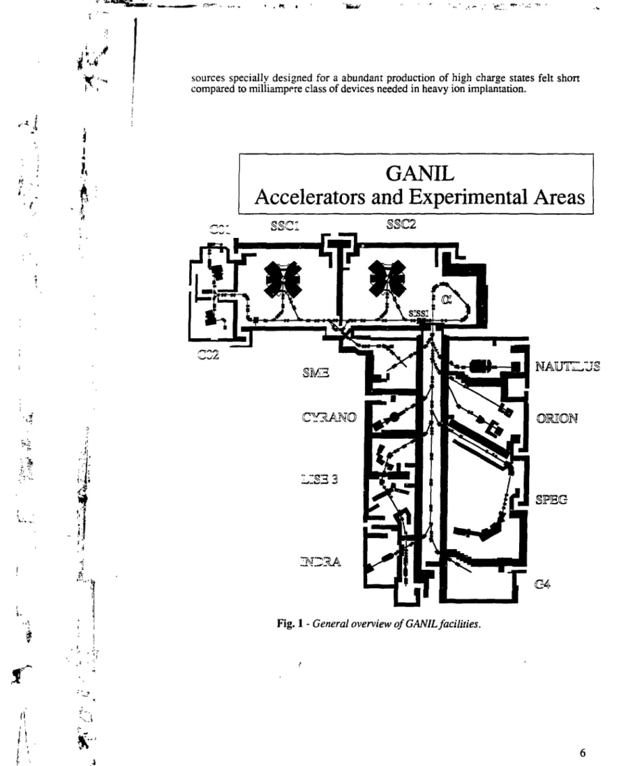
III. Overview of GANIL Facilities
After 10 years of exploitation, the main features of the G ANIL accelerators are well know. The modular structure of the GANIL facility (see Fig. 1) allows in principle to have access to heavy ion beams at low to high energy for the whole available ion spectrum ( C to U). First, there are two injector systems (denoted C01 and C02), each consisting of one Electron Cyclotron Resonance (ECR) source [17] coupled to a small compact cyclotron. The performances of GANIL ECR source are quoted in Table III. The maximum extraction voltage are 100 kV and 20 kV for the ECR sources associated to C01 and C02, respectively. The source with the highest extraction voltage is more devoted to metallic as well as heaviest mass ions. The intensities obtained with these
sources specially designed for a abundant production of high charge states felt short compared to milliampere class of devices needed in heavy ion implantation.
K
i,
• {
t
GANIL
Accelerators and Experimental Areas
ssc:
NAUTILUS
3 O 1 A
Fig. 1 - General overview of GANIL facilities.
K- ..
Table III - Performances ofGANIL ECR sources [18,19]. « • ' . ION Ar8+ Arl4+ Pb28+ Pb31+ U25+
BEAM CURRENT (e\iA)
580 5.5 22-100 8 32 v1 '• • Ï:
f
Ions extracted from the ECR source are then injected in a small compact cyclotron. Its role is to accelerate the ion beam to an energy witch matches the injection energy of the first separated sector cyclotron (SSCI). These energies lie between 0.3 MeV/u for the heaviest mass (HM) ions to 1 MeV/u for the lightest mass (LM) ones.
The ions are then accelerated by SSCI from 3 to 15 MeV/u for HM and LM ions respectively. After extraction from SSCI, the beam goes through a thin stripper foil which removed more electrons from these ions. After this stripping stage, the ions with higher charge states are injected in the second separated sector cyclotron SSC2. After ejection from SSC2, the energies are 6.25 times greater. They range from 25 MeV/u (for U) to 95 MeV/u (for C and O).
Also after the stripper foil, a beam with a lower charge state than the beam having the right property for injection in SSC2 can be deflected for use in a devoted experimental area (Dl). This medium energy beam line (SME, French acronym for "Sortie Moyenne Energy") is managed by CIRIL. Experiments with medium energy beams can be performed in the other GANIL experimental areas by using beams going only through SSCI (SSCI stand alone mode of operation).
A survey of recently accelerated beams with their characteristics is given in Table IV.
The most appropriate experimental devices are the G4 beam line and the irradiation set-ups IRASME (for SME) and IRABAT (for full energy) installed in Dl. These two latter devices are operated by CIRIL. All these installations are fully equipped with beam intensity and profile monitors. More details are given in Table V.
In G4 irradiation is performed in air inside a specially ventilated room. Any type of experimental devices can be installed in this room. The general lay out of the G4 beam line is given in Fig. 2. Starting from a well defined energy by the accelerator energies required by specific experiments can be adjusted by inserting dégrader foils and/or varying the air distance between the thin stainless steel window and the material to be irradiated. The values of these energies are calculated using range theory (see Refs. [20,21] and numerous references therein] and tables [22]. For example, in the case of membrane irradiations, if a ^~^Xe primary beam has an energy of 7.7 Mev/u, the beam will loose 3 MeV/u. through the stainless steel window and an air distance of 32 mm will be set to obtain the needed energy of 2.50 Mev/u entering the material to be irradiated. That corresponds then to the maximum value of the energy loss dE/dx in the middle of the material thickness, required to induce the largest defaults.
i
i fi • .*
1 ' ; Table IV - Features of recently accelerated beams at GANIL.
)
i
h
/ " ' À : Both cyclotrons combined ? ».- ft . * • i ft .A Ion 12c " 0 36A r ^4Kr 132xe 181T a 208P b 238ij 36A r 84^r 132Xe 181T a 208P b 238u 84Rr 129xe 208P b Charge before stripping 3 4 10 14 18 24 23 24 4 10 14 14 24 23 24 13 19 25 Charge after stripping Energy (MeV/u) Beam Intensity (enA)
Both cyclotrons combined 6 8 18 33 45 55 56 58 96.3 84.0 95.0 60.0 45.4 36.0 29.0 24.0 Medium Energy beam
7 17 32 43 54 53 55 12.2 13.6 9.0 6.8 6.0 4.6 3.8 Stand alone SSCI
9.1 7.7 5.4 2000 1250 800 1500 440 300 45 10 line 35 800 1200 350 170 180 80 2200 1060 400 (pps) 2.08 101 2 9.75 101 1 2.77 101 1 2.84 10H 6.10 101 0 3.40 101 0 5.02 109 1.08 109 3.12 101 0 2.94 10H 2.34 10H 5.08 101 0 1.96 101 0 2.12 101 0 9.08 109 1.06 101 2 3.48 10U 9.99 lOlO
Table V - Main characteristics from devices appropriate for industrial irradiations.
Irradiation condition Maximum irradiated surface Horizontal sweeping frequency1)
Vertical sweeping frequency Thermal control G4 beam line in air 500 x 40 mm2 L«ft)s=75 7 800 Hz IRABAT&IRASME 50: vacuum 30 x 30 mm2 x 50 mm2 (IRASME) 400 Hz 4 Hz 6 °K to 573 °K , " *
i4
f<*
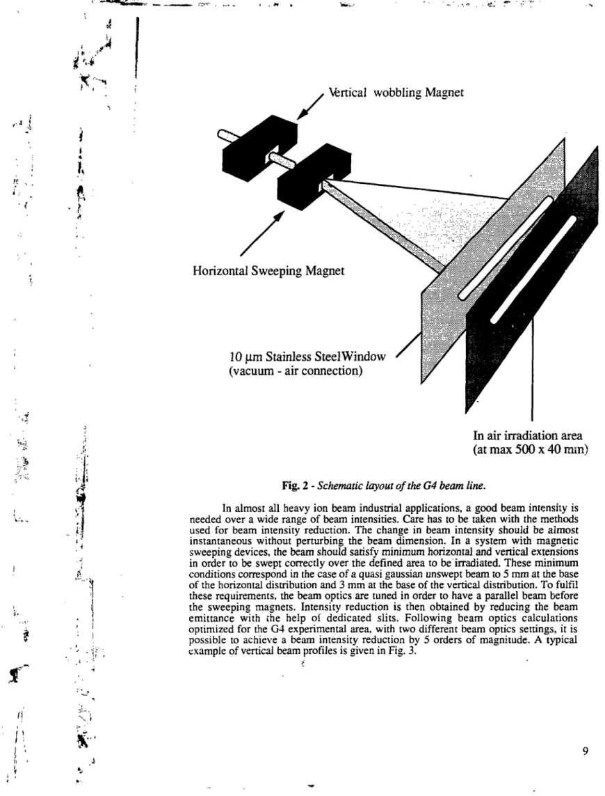
Vertical wobbling Magnet
Horizontal Sweeping Magnet
10 jim Stainless Steel Window
(vacuum - air connection)
In air irradiation area
(at max 500 x 40 mm)
5'.
1
•i
Fig. 2 - Schematic layout of the G4 beam line.
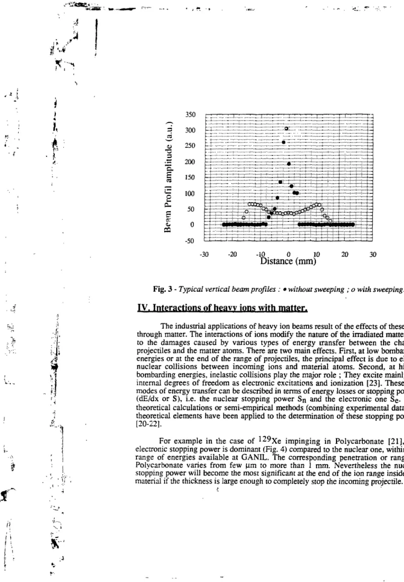
In almost all heavy ion beam industrial applications, a good beam intensity is needed over a wide range of beam intensities. Care has to be taken with the methods used for beam intensity reduction. The change in beam intensity should be almost instantaneous without perturbing the beam dimension. In a system with magnetic sweeping devices, the beam should satisfy minimum horizontal and vertical extensions in order to be swept correctly over the defined area to be irradiated. These minimum conditions correspond in the case of a quasi gaussian unswept beam to 5 mm at the base of the horizontal distribution and 3 mm at the base of the vertical distribution. To fulfil these requirements, the beam optics are tuned in order to have a parallel beam before the sweeping magnets. Intensity reduction is then obtained by reducing the beam emittance with the help ol dedicated slits. Following beam optics calculations optimized for the G4 experimental area, with two different beam optics settings, it is possible to achieve a beam intensity reduction by 5 orders of magnitude. A typical example of vertical beam profiles is given in Fig. 3.
£1 3
S
350 300 250 200 150 100 50 0 -50 t-t • : i i i - *• o - ••• r - - • - r , , i..-,...^...-v «...-ii v- v—•> ^ . - . - ; . - . ; . . . ^ . {... " "* " " " * "" ~Mk: '• ~ '•' ••—-:••" - * * -•— • • • * — ....— '—':. r—i T..»™...., ;..-i v. ....i.. .;...„.. -;..^..^..;.-4...i...:]ii...U..;..._...r.^i...i.-.i...:...ZâL.i..., ...;...T...r..:...r...r...r..r.r..r...;...T...:...T...:...r.r..;...r ..-•{...•*•—}... - . — ._ . . _ i 1 i i i i 1 i î î i | ! ! r Ml ] K i • -30 -20 -10 0 10 20
Distance (mm)
30 • I 4Fig. 3 - Typical vertical beam profiles : • without sweeping ; o with sweeping.
IV. Interactions of heavy ions with matter.
The industrial applications of heavy ion beams result of the effects of these ions through matter. The interactions of ions modify the nature of the irradiated matter due to the damages caused by various types of energy transfer between the charged projectiles and the matter atoms. There are two main effects. First, at low bombarding energies or at the end of the range of projectiles, the principal effect is due to elastic nuclear collisions between incoming ions and material atoms. Second, at higher bombarding energies, inelastic collisions play the major role ; They excite mainly the internal degrees of freedom as electronic excitations and ionization [23]. These two modes of energy transfer can be described in terms of energy losses or stopping powers (dE/dx or S), i.e. the nuclear stopping power Sn and the electronic one Se. Pure
theoretical calculations or semi-empirical methods (combining experimental data and theoretical elements have been applied to the determination of these stopping powers [20-22].
For example in the case of 129xe impinging in Polycarbonate [21], the electronic stopping power is dominant (Fig. 4) compared to the nuclear one, within the range of energies available at GANIL. The corresponding penetration or range in Polycarbonate varies from few |Ltm to more than 1 mm. Nevertheless the nuclear stopping power will become the most significant at the end of the ion range inside the material if the thickness is large enough to completely stop the incoming projectile.
10
"M'
•n Mi - • • f r v N 1l\
3 o s 10000 100 •o LU 0.01 129Xe in Polycarbonate
Electronic stopping ^ . ^ - """" Range Nuclear stepping 0.1 1 10 Energy (Mev/u) 100Fig. 4 - Stopping powers dEldx (MéV crn^/mg) and Range (pan) of
129Xe in polycarbonate as a function of beam energy (MeV/u).
1- Latent tracks
During the projectile slowing down process due to the present interactions previously described, creation of defects and cascades of defects occurs along its trajectory. These defects lead to latent tracks [6,23,24]. The core of latent tracks corresponds to a highly perturbed zone of roughly 10 nm in diameter. Various models have been put forth to explain its origin (see Spohr [6] and references therein). Associated to track core, there is a track halo resulting of the propagation of electronic collisions. This halo could extend up to 1 |im around the track core. Even if the applications of latent tracks in solids have been known for quite a long time [24], more fundamental investigations are still a very active field of research around the world [6].
The latent tracks are much more sensitive to chemical etching than the bulk of the material. In such circumstances, a chemical etching with appropriate reagents will induce the appearance of micrometric pores. The size of these pores can be controlled by appropriate choices of irradiation conditions, etching features (time, temperature) and reagent nature [6,24].
2- Damages induced by Elastic collisions.
At low ion energy, the nuclear collisions can produce radiation damages as the direct energy transfers to the struck atoms induce atomic displacements in cascade. These radiation damages would be responsible for corrosion and fadgue in stainless steel alloys. For example 10*18 to 10*1' displacement per atom (dpa) is produced by a 9 Mev/u Kr projectile in isuch materials [25]. For comparison sake a fast neutron will induce only 10*21 t 0 io-2O ^pa. i.e. three orders of magnitude less. Furthermore, the
primary knock-out atomic spectra are very similar in both cases [25,26]. In such circumstances, heavy ion irradiations are a very good tool to simulate defects created by
I*
11
fast neuirons in various alloys. To get 1 dpa, 10 hours of a Kr beam (at 1 |iAe) aie only needed. I
i
i "I \ t ÏV. Tests of radiation hardened electronics components.
When a heavy ion travels through an electronic component, the phenomena just described take place. Atom displacements due to nuclear elastic collisions at low energy and ionization at higher energy occur along its path. A solid state silicon detector will react in the same way [27]. These phenomena perturbed the normal behaviour of the component and lead to two main effects [28,29]: soft errors like single event upsets (SEU) or potentially damaging ones like latch-ups (LU) and power transistor burnout (BO). The intense ionization along the ion path generates charges inducing non destructive changes in the logic states of the circuit in case of SEU.
Different electronic component companies [28,29] have designed technologies hardening these components against radiation influence. In order to qualify the hardening quality, designers or users must perform series of irradiation with the various types of radiation corresponding to the normal environment of the components. For circuits dedicated to spatial missions, heavy ion irradiation is in order as they are present in the cosmic rays. Furthermore the very compact size (to avoid too much weight in flight) of spatial components render them quite sensitive to such radiation.
I ; et S * 1000 100 10 0.1 2 3 8U (80-150 |im) (60-680 4 0 , Ar (60-1200 1 2C (100-3000 fim) 10
Beam Energy (MeV)
100
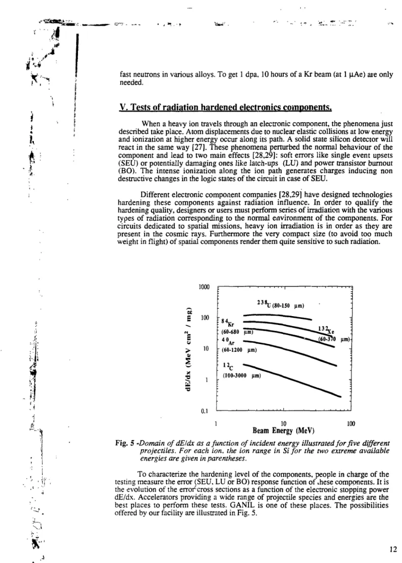
Fig. 5 -Domain of dEldx as a function of incident energy illustrated for five different
projectiles. For each ion, the ion range in Si for the two extreme available energies are given in parentheses.
To characterize the hardening level of the components, people in charge of the testing measure the error (SEU, LU or BO) response function of these components. It is the evolution of the errorcross sections as a function of the electronic stopping power dE/dx. Accelerators providing a wide range of projectile species and energies are the best places to perform these tests. GANÏL is one of these places. The possibilities offered by our facility are illustrated in Fig. 5.
X:
i
,-Stopping power values range from 0.3 to more than 100 MeV cm2/mg, i.e. 3
orders of magnitude. The most often ions requested by our main partner MATRA MARCONI SPACE (MMS) France are Ar, Kr and Xe [30].
An error response function is determined by measuring the error cross sections (proportional to the number of errors per incident ions) for various energies corresponding to different dE/dx values. After a dE/dx threshold, the error response function starts to raise and tend to level off afterwards (see a typical example in Fig. 6). In this case the dE/dx threshold is equal to 8 Mev cnvtymg. The higher is this threshold, the better is the hardening quality.
10',-4 3 CO
1
2
uua
C/5 10-5 10-6 10-764K PROM R29793
• i i .r
20 40 60 80 100Electronic stopping power (MeV cm /mg)
Fig. 6 - S£t/ response function for a the 64K PROM R29793 [30]. The line drawn isjust to guide the eyes.
The prediction of the behaviour of the electronic component in space if the main goal of the tests performed by MMS. The empirical computation of the various error rates for various orbits takes into account the error response function of the component, its electrical and geometrical characteristics and the radiation levels corresponding to the considered orbits (see [30] and references therein).
Recent tests performed by MMS have revealed that at high dE/dx values, high density S RAMS have presented a new type of perturbations [31] induced by one single ion. It corresponds to the appearance of jammed bits in the memory. These defects are very hard to detect and to:'correct. This new effect was called a single hard error (SHE).
Space electronic designers face then a real challenge and will haveto cope with SHE in the context of the still growing level of integration for electronic devices.
•*J
i
VI. Status of Present Industrial Applications.
To the applications selected after the market study previously described (see Table 1 ), two new programs have undertaken after motivated requests of industrial companies. All ongoing activities will be quickly reviewed in this section. Technology transfers not connected to heavy ion irradiation will be also invoked. They result of activities linked to operations of the accelerators, development projects and designs of experimental devices.
1- Nuclear track membranes.
This activity has not reach the level predicted by the study market due to an unexpected technical problem (mechanical strength in certain circumstances) with polycarbonate, the most common polymer used in this sector. At present irradiation is performed for a German company specialist of other polymers as Polyethylene terephtalate PET [32]. Furthermore, in the case of the acceptance by the European Community of a proposed BRITE EURAM II project on specially designed nanofiltration membranes, GANIL and GSI will provide appropriate heavy ion beams.
A collaboration is underway with a French "Tissue Engineering" firm. Its main object concern the investigation of the best means to render microporous some materials of biological interest.
We collaborate also in this field with a French company expert in products involving rubber with the objective to find a microporous material film with a high adhesion power. The adhesion has to take place between this film and rubber.
These last two applications are really plan to get results if any on the long range.
>"•• :
i :
• s
Hi
4
2- Fluorescent flat screens with field emitter microtips.
As already quoted in the description of IA survey study, nanofabrication and microelectronics lithography with heavy ion beams possess many apparent advantages. Nowadays luminescent flat screens [33] with field emitters cathodes [34] have realized with standard U. V. lithography. This technique has been pushed to its limits in terms of line widths but the future of this application to large area is dim from my own point of view. On the contrary heavy ion lithography does not suffer from a large scale limitation owing to first physical principles.
The first tests realized in this direction are conclusive and it's all I am permitted to say. If the technique is proved successful, its paramount importance for High Definition Television screens speaks by itself. We collaborate on this subject with the promoter of this technique (CEA/DTA/LETI, Grenoble).
1 ' 1
3- Heavy Ion Adhesion Enhancement.
This theme came out of the market study. The literature is very abundant on that matter [3]. Recent results from a GSI group [4,5] in the case of very heavy ions (e.g. Bi) are very promising but older works were not so conclusive. Furthermore the field of adhesion is highly active nowadays and various physical and chemical competing techniques are emerging. More fundamental research and development are in order. We are analyzing with CIRIL and potentially interested firms, the best ways to strengthen this activity on the GANL site. A collaboration with GSI within the framework of our mutual agreement on heavy ion applications is seek for.
4- Tribology.
14
i
i .
i
Nuclear techniques (e.g. panicle induced material activation) are widely present in tribology methods. The use of radioactive directly implanted species appears as their natural extension [35]. Such methods have been tested with success on low Z material as ceramics [36]. Implantation of ^Be presents various advantages (long half live, easy y ray detection). Plastics of growing economical importance are difficult to analyse in this respect. The methods and the deep implantation conditions are under analysis with CIRIL and CEA/DTA/DAMRI. Already the resistance of various plastics to fluences to be used has been investigated.
5- Simulation of neutron damages in alloys.
As mentioned previously heavy ion irradiation is quite effective to simulate the effects of neutron bombardment on Stainless Steel alloys. These alloys are main components in Pressured Water Reactors PWR. The neutron damages lead to wear and increased corrosion resulting in a more rapid ageing of these alloys and by consequent of PWRs. This is a ongoing program involving CIRIL and the French Electrical company EDF.
6- Technology transfers.
To sustain a high level of performances for its accelerators and to insure the success of the experiments performed, GANIL is engaged in a series of developments in ion sources, accelerator technology and instrumentation (i.e. electronics). New products or modules are often designed and realized to achieve these missions. The policy of GANIL is to transfer as often as possible to industries such products and modules. The reduced size ECR source NANOGAN® is a typical example. Such an ion source could find applications for high energy implanters and licenses have been granted. Similar technology transfers and licensing are common for electronics modules used for experiments.
VII. Summary
Heavy ion industrial applications have been going on since 1983. Its importance bas been analyzed lately with a marketing approach to reinforce its impact on industries of various sectors. With the help of this pragmatic approach the main themes have been re-focused and their number limited to improve overall efficiency. Today there are five well defined operational applications. Since the end of the strategy study two new industrial applications were triggered upon request from outside.
So far only beams delivered by one or both cyclotrons have been used. Beams at injector energies would be helpful to perform preliminary tests with the constraint of working under vacuum. In certain cases this possibility will render the access to beams easier. As the number of experiments performed is still rather large, the GANIL beam co-ordinator faces important constraints and fast delivery to our industrial partners can be guarantee. In the event of a significant GANIL upgrade to produce radioactive beams, the new accelerator could be used with profit stand alone off radioactive beam scheduled period. Other advantage of this possibility would may well be a reduction in operation cost. '"
Acknowledgements.
i .
Besides SAIF group many people contribute to the success of industrial applications at GANIL. I would like to deeply thank C. Bieth the fervent IA advocate and the guide of my first steps in this game, J.L. Ciffre, J.C. Foy, J. Cacitti, the "Aires Expérimentales" group, the accelerator operating staff, the whole CIRIL personnel and M. Toulemonde in particular, and many others I certainly unjustly forgot but without malice.
References
[II- J.B.A. England, International Conference,Proceedings of Applications of Nuclear Techniques, Heraklio, Crete, Greece, June 1990, G. Vouivopoulos and T. Paradellis (Editors), World Scientific Publishing Co (1991), pp 10-29.
[2] - B.E. Fischer, Nucl. Instr. Meth. 2J6,265 (1983)
[3] - J.E.L. Baglin, NucJ. Instr. Meth. Phys. Res. B65,119 (1992)
[4] - L. Wang, Ch. Trautmann, J. Vetter, Z. Quan, D. Cohen and H. Fladry, Rad. Effe Eff. Def. in Solids 126,403 (1993)
[5] - L. Wang, N. Angert, D. Ruck, Ch. Trautmann, J. Vetter, Z. Quan and H. Hantsche, submitted to Nucl. Instr. Meth. Phys. Res. (submitted)
[6] - R. Spohr, Ion tracks and Microtechnology
Principles and Applications, Klaus Bethge Ed., Vieweg, 1990
[7] - T.C. Yang, G. Welch, C.A. Tobias, H. Maccabee, T. Hayes, L. Craise, E. V. Benton, F. Abrams, Annals of the New York Academy of Sciences, 306. pp 3322 - 339 (1978)
[8] - B.E. Fischer and R. Spohr, Nucl. Inst. Meth. 168,241 (1980) [9] - S.T. Picraux, Ann. Rev. Mater. Sci. 14,335 (1984)
[10]- G. Dearnaley, P.D. Goode, F. J. Mimer, A.T. Peacock, W. Hughes and G.W. Praetor, Vacuum 36, 807 (1986)
[11]- G. Dearnaley, Nucl. Instr. Meth. Phys. Res. B50,358 (1990) [12]- N.E.W. Hartley, Tribology international, 65 (1975)
[ 13] - T. W. Conlon, Contemp. Phys. 26,521 (1985) [ 14] - B. Coss Levi, Physics Today 21, Oct, 17 (1991) [15] - L. Curam, Electronics 64,10,48 (1991)
[16] - C. Morgan, G.S. Chen, C. Boothnoyd, S. Bayley and C. Hamphreys, Physics World Vol 5.11,28 (1992)
[17] - R. Gdler, Annu. Rev. Nucl. Sci. 40,15 (1990)
[18]- M.P. Bourgarel et al., Proceedings EPAC90, Nice, June 1990
[19] - P. Sortais et al., Proceedings of the 10th International Workshop on ECR Ion Sources, Knoxville, USA, Nov. 1990.
[20] - J.F. Ziegler, J.P. Biersack and U. Littmark, The Stopping and Ranges of Ions in Solids, Pergamon Press, New York, 321 pp., 1985.
[21] - J. F. Ziegler and J.M. Manoyan, Nucl. Instr. Meth. Phys. Res. B35. 215 (1988).
[22] - F. Hubert, R. Bimbot and H. Gauvin, At. Data & Nucl. Data Tables 46, 1 (1990)
[23] - E. Baianzat and S. Bouffard, Contribution to "Materials under Irradiation" Summer School, Giens, France, Sept. 1991, CIRIL Report, March 1992. [24] - R.L. Fleischer, P.B. Price and R.M. Walker, Nuclera Tracks in Solids :
Principles and Applications, University of California Berkeley, 1975. [251 - S. Bouffard and J. C. Jousset, Private communication, 1993
126] - G. Bardos, Phys. Lett Al 19,415
[27] - P.J. McNulty.'W,G. Abdel-Kader and J.E. Lynch, Nucl. Instr. Meth. Phys. Res. B61, 52 (1991)
|281 - L. Adams and A. Holmes-Siedle, La Recherche 236,1183 (1991)
129] - L. Adams and A. Holmes-Siedle, Nucl. Instr. Meth. Phys. Res. A314. 325 (1992)
f
S.T
'•"À
xn
I .
[30] - c. Dufour. P. Gamier, J. Beaucour and H. Delagrange, 29t h Annual
International Nuclear and Space Radiation Effects Conference, IEEE, New Orleans, LO, Usa, July 13-17, 1992, Poster W-7.
[31]- C. Dufour, P. Gamier, T. Carrière, J. Beaucour, R. Ecoffet and M. Labrunée, 29t n Annual International Nuclear and Space Radiation Effects
Conference, IEEE, New Orleans, LO, USA, July 13-17,1992.
[32] - H.B. Liick, H. Marines, B. Gemende, B. Heinrich, W. Pfestorf, W. Seidel andS. Turuc, Nucl. Instr. Meth. Phys. Res. B50, 395 (1990)
[33] - A. Ghis, R. Meyer, Ph. Rambaud, F. Levy and Th. Leroux, Third International Vacuum Microelectronic Conference, Monterey, USA, July
1990.
[34] - J.K. Cochran, A.T. Chapman, D.N. Hill and K.J. Lee, J. Mater. Res. 2, 322 (1987)
[35] - T.W. Conlon, Tribology Int. April 1979.
[36] - M.L. Malîory, R.M. Ronningen, Wm. C. Harris, B. Sherrill X.Y. Dardenne and H.J. Schock, Nucl. Instr. Meth. Phys. Res. B40/41. 549 (1989)
;*=*.

![Table II - High quality features of heavy ion lithography (taken from [6]).](https://thumb-eu.123doks.com/thumbv2/123doknet/12930210.374023/7.1111.103.946.61.1155/table-ii-high-quality-features-heavy-lithography-taken.webp)

![Fig. 6 - S£t/ response function for a the 64K PROM R29793 [30]. The line drawn is just to guide the eyes.](https://thumb-eu.123doks.com/thumbv2/123doknet/12930210.374023/15.1110.122.964.61.1204/fig-response-function-prom-line-drawn-just-guide.webp)
