Design and Control of Photoflash Capacitor
Charging Circuits
by
Michael G. Negrete
Submitted to the Department of Electrical Engineering and Computer
Science
in partial fulfillment of the requirements for the degree of
Masters of Engineering in Electrical Engineering and Computer
Science
at the
MASSACHUSETTS INSTITUTE OF TECHNOLOGY
January 2004
c
° Linear Technology Corp, MMIV. All rights reserved.
The author hereby grants to MIT permission to reproduce and
distribute publicly paper and electronic copies of this thesis document
in whole or in part.
Author . . . .
Department of Electrical Engineering and Computer Science
January 16, 2004
Certified by . . . .
Albert M. Wu
Design Engineer
VI-A Company Thesis Supervisor
Certified by . . . .
David J. Perreault
Assistant Professor
M.I.T. Thesis Advisor
Accepted by . . . .
Arthur C. Smith
Chairman, Department Committee on Graduate Students
Design and Control of Photoflash Capacitor Charging
Circuits
by
Michael G. Negrete
Submitted to the Department of Electrical Engineering and Computer Science on January 16, 2004, in partial fulfillment of the
requirements for the degree of
Masters of Engineering in Electrical Engineering and Computer Science
Abstract
This thesis develops an optimal strategy for charging photoflash capacitors. Photoflash capacitors need to be charged to voltages as high as 350V in low-voltage battery-powered portable devices. With the decreasing size of digital cameras, existing so-lutions are too large. This thesis will study the operation and losses of a flyback capacitor charger. Specifically, the thesis will focus on minimizing the solution size, given an input current, in addition to keeping efficiency acceptable.
VI-A Company Thesis Supervisor: Albert M. Wu Title: Design Engineer
M.I.T. Thesis Advisor: David J. Perreault Title: Assistant Professor
Acknowledgments
This thesis would not have been possible without assistance of the people below. First, I would like to thank Albert Wu and Steve Pietkiewicz for proposing the idea behind this thesis. Albert Wu served as a great mentor and supervisor. I learned a great deal from his expertise in the area of circuit design and power electronics and this will continue to benefit me in the coming years. I would like to thank Professor Perreault for volunteering to be my thesis advisor with his already tremendous work load. He gave many insightful comments to some of the ideas presented in my thesis well before the ambitious deadline I set for myself. There are many other individuals that served as valuable sources of information at Linear Technology that I would like to thank too. This thesis would not be possible without the support from Linear Technology and Dave Bell. Dave Bell always made sure my project was exciting and relevant throughout my VI-A internship. And last but not least, I could not have done such a professional job on the diagrams without assistance from Ilyssa Lu.
I would also like to thank all my family and friends that have supported throughout my life, especially when times have been tough. I extend my biggest thanks to my parents, who have served as a crucial role model and inspiration throughout my life. My father has encouraged a curiosity about how things work at an early age, and this has done wonders to my ability to excel at engineering. I credit my mother for helping me develop the personal skills needed to get through life and always trying to keep me humble. I would also like to thank my sister for giving me some of her enthusiasm.
Contents
1 Introduction 17
1.1 Background . . . 17
1.2 Overview . . . 18
1.3 Organization . . . 20
2 Operation of a Flyback Converter 23 2.1 Theory . . . 23
2.2 Transformer . . . 27
2.3 Power Switch . . . 27
2.4 Diode . . . 28
2.5 Boundary Mode Operation . . . 28
2.6 Linear Technology Flyback Capacitor Chargers . . . 30
3 Modeling a Flyback 33 3.1 Introduction . . . 33
3.2 Losses associated with the switch . . . 34
3.2.1 Switch Resistance Losses . . . 34
3.2.2 Losses due to Rise and Fall Time of Switch . . . 35
3.3 Losses from Transformer . . . 36
3.3.1 Loss from Leakage Inductance . . . 36
3.3.2 Loss from DC Winding Resistance . . . 37
3.3.3 Core Loss . . . 38
3.4 Diode Losses . . . 39
3.5 Charge time . . . 41
4 Modeling in MATLAB 43 4.1 Introduction . . . 43
4.2 Calculating Individual Losses . . . 43
5 Design, Construction and Testing of a Flyback Capacitor Charger 49 5.1 Introduction . . . 49
5.2 Design . . . 49
5.3 Construction . . . 53
5.4 Debugging . . . 54
5.5 Boundary Mode Operation . . . 54
5.6 Final Product . . . 55
6 Transformer Optimization 57 6.1 Introduction . . . 57
6.2 Transformer Basics . . . 57
6.3 Hand-winding Transformers . . . 60
6.4 Measuring Inductance Values for Transformer π Model . . . . 61
6.5 Effects of Leakage Inductance . . . 61
6.6 Effects of the Transformer’s Capacitance . . . 65
6.7 Energy Storage Requirements . . . 66
7 Experimental Results 69 7.1 Introduction . . . 69
7.2 Correlation of Simulated and Measured Data . . . 69
7.3 Magnetizing Inductance . . . 71
7.4 Alpha Comparisons . . . 77
7.5 Turns Ratio . . . 81
7.6 Scaled Transformer Core . . . 83
8 Flash Unit 91
8.1 Introduction . . . 91
8.2 Self-Oscillating Capacitor Charger . . . 91
8.3 Xenon Bulb . . . 93 8.4 IGBT . . . 96 9 Conclusion 99 9.1 Summary . . . 99 9.2 Further Work . . . 99 A MATLAB Code 101 B Board Layout 109
List of Figures
1-1 Generic flyback converter. . . 19
2-1 Flyback converter. . . 24
2-2 Primary current waveform. . . 24
2-3 Secondary current waveform. . . 24
2-4 Magnetizing inductor current. . . 26
2-5 Second order network when switch turns on. . . 29
3-1 Magnetizing inductor current. . . 34
3-2 Primary current waveform. . . 34
3-3 Switch turn off waveform. . . 35
3-4 Switch turn on waveform. . . 35
3-5 Secondary current waveform. . . 37
3-6 Scope shot: Ch4 is primary switch pin. . . 40
3-7 Diode reverse recovery current. . . 40
4-1 Breakdown of losses from a typical flyback charger (Part 1 of 2). . . . 44
4-2 Breakdown of losses from a typical flyback charger (Part 2 of 2). . . . 45
4-3 Efficiency curve for flyback converter with alpha=0 and L=24uH. . . 46
4-4 Efficiency versus magnetizing inductance. . . 48
5-1 Flyback capacitor charger test circuit. . . 50
5-2 Simulated primary and secondary currents of test circuit. . . 52
5-3 Circuit diagram of the boundary mode controller. . . 55 5-4 Scope shot: Ch1 is output voltage, and Ch3 is input current(.25A/div). 56
6-1 Transformer model. . . 60
6-2 Scope shot: Ch3 is primary current (AC coupled, .1A/div), and Ch4 is switch voltage. . . 63
6-3 Scope shot: Ch2 is secondary winding Pin, and Ch3 is secondary wind-ing current. . . 63
6-4 Scope shot: Ch3 is real primary current (ac coupled, 1A/div), and Ch4 is primary switch pin. . . 64
6-5 Scope shot: Ch3 is real secondary current (inverted, 100mA/div), and Ch4 is primary switch pin. . . 65
6-6 Scope shot: Ch1 is amplified primary current(1A/div), Ch2 is amplified secondary current(100mA/div), and Ch4 is primary switch pin. . . . 66
6-7 Magnetizing inductance increase with α. . . . 67
7-1 Efficiency versus output voltage for L=10uH and α = 0. . . . 72
7-2 Efficiency versus output voltage for L=10uH and α = 0.1. . . . 72
7-3 Efficiency versus output voltage for L=16uH and α = 0. . . . 73
7-4 Efficiency versus output voltage for L=16uH and α = 0.1. . . . 73
7-5 Efficiency versus output voltage for L=16uH and α = 0.2. . . . 74
7-6 Efficiency versus output voltage for L=24uH and α = 0. . . . 74
7-7 Efficiency versus output voltage for L=24uH and α = 0.2. . . . 75
7-8 Efficiency versus output voltage for L=24uH and α = 0.4. . . . 75
7-9 Efficiency versus output voltage for L=24uH and α = 0.6. . . . 76
7-10 Inductance versus efficiency. . . 78
7-11 Efficiency versus alpha with variable gap length. . . 79
7-12 Efficiency versus alpha with fixed gap length. . . 80
7-13 Maximum frequency versus alpha with variable gap length. . . 80
7-14 Maximum frequency versus alpha with variable turns. . . 81
7-15 Efficiency curves with different turns ratios. . . 82
7-16 Efficiency versus volume factor. . . 84
7-18 Magnetizing inductance versus volume factor. . . 85
7-19 Primary peak current versus volume factor. . . 85
7-20 Scope shot: Ch1 is secondary current waveform(100mA/div), and Ch4 is switch waveform. . . 87
7-21 Scope Shot: Ch1 is primary current(1A/div), and Ch3 switch waveform. 87 8-1 Self-oscillating capacitor charger circuit diagram. . . 91
8-2 Xenon triggering circuit. . . 94
8-3 Xenon triggering waveform. . . 95
8-4 Xenon bulb current. . . 95
8-5 IGBT circuit. . . 96
8-6 Illustrative IGBT waveforms. . . 97
List of Tables
4.1 Table of inputs to total efficiency function for flyback charger. . . 47 7.1 Total efficiency using capacitor energy method. . . 71 7.2 Equivalent switch capacitance effects with turns ratio. . . 82
Chapter 1
Introduction
1.1
Background
This thesis develops an optimal strategy for charging photoflash capacitors. Two ICs developed by Albert Wu at Linear Technology, LT3420 [2]and LT3468 [1], inspired the ideas presented in this thesis. These ICs implement two different charging strategies, both focusing on shrinking the solution size while improving the efficiency over previ-ous charging methods. Only one other significant research paper, by Sokal, has been written on charging capacitors. In [5], Sokal comes to a conclusion on the fastest and most efficient method to charge a capacitor given a maximum peak switch current. The techniques developed in this thesis are most applicable to charging photoflash capacitors in digital cameras.
Before the wide spread use of electronics, cameras used individual flash bulbs or flash bars to produce a 40ms pulse of intense white light from a chemical reaction. About 40 years ago, professional photographers started to use electronic flashes with a much shorter 1ms pulse of white light, generated using a Xenon bulb. Electronic flashes were not used extensively until the last 10 years when all but the cheapest cameras utilize them as standard equipment. With improvements in technology in the last ten years, cameras have decreased considerably in size. The smallest digital camera is the size of a 1
4 inch thick credit card. Cell phones now feature built-in
space as a premium in camera cases, the size of the flash capacitor charger is critical to its utility.
Currently, popular methods to charge a photoflash capacitor include the oscillating forward converter and the micro-controlled flyback converter. The self-oscillating forward converter is comparatively the most cost effective, since it requires only a few discrete transistors. However, it is inefficient at low voltages and the custom multi-winding transformers are too bulky for the increasingly feature-packed digital and film cameras. This type of charger is only found in disposable and inexpensive film cameras. Most other cameras produce a flash with a microprocessor-controlled flyback converter. It controls the gate of a power switch with a pre-programmed set of switch on and off times with only the ability to detect the primary current and the output voltage. Since the controller cannot sense secondary current, the controller has to store an algorithm to calculate an appropriate switch off-time. If the secondary current decays to zero before the end of the off-time, the circuit will remain idle which increases the peak-current requirements, thus it enlarges the transformer and the switch.
Clearly, a more effective method of charging capacitors exists. This thesis will explore the variable frequency control methods explained in [5], but apply them to the rapidly expanding market of digital cameras.
1.2
Overview
To generate a flash, a Xenon flash bulb requires a special capacitor charged to a high voltage. This thesis will study methods to charge this photoflash capacitor from a low input voltage with a power limit. The required capacitance is determined by the size of the flashbulb. [7] Without variations in efficiency, the charge time is set by the final output voltage, the output capacitance, and the input power. As a result of this dependency, this makes solution size and efficiency the most important features of a capacitor charger. This thesis will focus on analyzing flyback capacitor charger performance normalized to a given input power specification.
A flyback converter consists of a transformer, switch, diode, output capacitor and control circuitry. Figure 2-1 shows the configuration of a flyback converter. The transformer serves as the energy storage device. With the switch on, the trans-former’s magnetizing inductance magnetizes from the input power source. The input voltage determines the rate of magnetization. When the core of the transformer be-comes close to saturation, the switch turns off, forcing the transfer of current from the transformer’s primary winding to the secondary winding. The current from the secondary winding flows through the diode to the output capacitor. Depending on the charging strategy, the switch might turn on to terminate the current to the output capacitor before the secondary current falls to zero. The secondary winding has more turns than the the primary winding to limit the voltage the switch has to withstand.
Vin
1:N Vout
Figure 1-1: Generic flyback converter.
In a flyback converter with ideal components, the amount of magnetizing induc-tance would not affect the charge time of the charger, but would only determine the operating frequency. With stray capacitances on the switch node and core losses, efficiency decreases with increased operating frequency. Therefore, a magnetizing in-ductance should be determined to keep the operating frequency below a maximum operating frequency. This maximum operating frequency would be dependent on the type of core material used and the amount of stray capacitance on the switch node. Although losses from the core and the stray capacitance decrease with larger magnetizing inductance, more turns are needed for both the primary and secondary
windings, thereby increasing the winding resistance. An accurate model of these losses is needed to determine the optimum amount of magnetizing inductance.
All the loss terms for a flyback charger may be easily derived analytically as a function of the output voltage. These equations could be added together analytically, but would result in a large, un-intuitive equation. Instead, MATLAB is used to plot, sum and integrate these equations numerically. MATLAB is also capable of converting a power loss in terms of Vout to a total charge cycle efficiency. This thesis
will rely on MATLAB to plot total efficiency versus parameters such as magnetizing inductance. The calculations done in MATLAB will focus the experimentation and be correlated with actual data afterwards.
For the experiments, a flyback controller was built with adjustable primary and secondary current limits. The primary and secondary currents are measured with sense resistors and op amps. With control over both current limits, the controller is capable of keeping the maximum input current constant with all the charging strategies. The controller is also capable of turning the switch on by monitoring the switch node voltage instead of the secondary current. The flyback capacitor charger is flexible enough to use a wide range of transformers. These transformers have different magnetizing inductances, turns ratios, winding window allocations, and core gap lengths. A TDK EPC10 core is used for all of the experiments. [6]
1.3
Organization
In Chapter 2, the thesis explains the operation of a flyback capacitor charger and the benefits of variable-frequency operation. The components are also discussed briefly. In Chapter 3, the flyback chargers losses are modeled analytically, along with the charge time. Chapter 4 outlines the techniques used in MATLAB to compute losses with the analytical models. From there, Chapter 5 describes the construction and testing of a flyback capacitor charger. Chapter 6 analyzes the transformer in detail. Chapter 7 compares the experimental results with the simulations and also suggests optimal values for components. Chapter 8 is an overview of the components used to
create a flash in a digital camera. Finally, conclusions and suggestions for further work are discussed in Chapter 9.
Chapter 2
Operation of a Flyback Converter
2.1
Theory
A flyback converter, as shown in Figure 2-1, consists of a transformer, a power transis-tor, a diode, and an output capacitor. The following description of a flyback converter is valid for one that regulates or charges. The switch turns on to allow the current in the magnetizing inductance of the transformer to reach a peak value, Ilim, as shown in
Figure 2-2. The slope of the current in the charging pulse is constant over the charg-ing cycle. When the switch turns off, the magnetizcharg-ing inductance delivers current to the output capacitor through the secondary winding; this time period is known as the flyback period. The peak secondary current is N times smaller than the primary cur-rent, as shown in Figure 2-3. As the output voltage increases, the secondary current decreases faster. Psw = 1 T Z T 0 RswIsw2 dt = dIlim2 Rsw[α + 1 3(1 − α) 2] (2.1)
Most regulating flyback converters operate in a constant-frequency control mode. With a constant-frequency, the steady-state duty cycle is determined solely by the input voltage, output voltage, and the turns ratio. However, with a light load, the converter enters discontinuous mode and the duty cycle relationship is no longer valid. Discontinuous mode occurs when the magnetizing current falls to zero before
Vin
1:N Vout
Figure 2-1: Flyback converter.
0 dT T αIlim Ilim -6 Isw t
Figure 2-2: Primary current waveform.
0 dT T αIlim/N Ilim/N -6 Isw t
the switch turns on again. In discontinuous mode, the duty cycle controls the average current to the output capacitor. In lieu of duty cycle control, many regulators control duty cycle implicitly by controlling the peak current in the primary winding which allows converters to operate in either continuous or discontinuous mode. Converters use a sense resistor between the emitter of the switch and ground to sense the peak current. The peak current limit is adjusted by sensing if the output voltage is above or below the set output voltage.
Constant-frequency control works efficiently with a constricted output voltage range, but in the charging of a capacitor, the output voltage ranges from 0 volts to the final output voltage which could be as high as 500 volts. The voltage across the secondary winding varies drastically, resulting in off-times that vary by a 500:1 ratio. At low voltages, the duty cycle will become very small and will approach the minimum on-time of the controller. Once the minimum on-time is reached the part can no longer return the magnetizing current to the level at the start of the switch cycle. The magnetizing current will increase with every switching cycle. To limit current, the regulator will need to be capable of skipping cycles to let the secondary current fall below the current limit which will in turn reduce the switching frequency. At high output voltages, the secondary current falls fast compared to switch on-time. As a result, the secondary current falls to zero before the end of the switching period, leaving the circuit in an idle state, which leads to higher peak currents for a given input power. At both low and high output voltages, undesirable operation occurs when implementing constant-frequency control for charging capacitors.
To operate more efficiently in capacitor charging, the flyback converter should operate with a variable frequency. Without a set switching frequency, the circuit determines when to end the flyback period. As in the constant-frequency case, the switch turns off once the primary winding current reaches a current limit. One method to determine when to terminate the flyback period involves sensing the secondary winding current. The switch is turned back on once the current falls to a fraction of the current limit. This technique is shown in Figure 2-4 where α is the ratio of the secondary current to the primary current. In [5], Sokal and Redl discuss flyback
charging circuits. They conclude that an α close to unity, producing flat current pulses to the output capacitor, minimizes peak and RMS currents, thus reducing losses associated with parasitic resistances and current-carrying requirements of the switch, transformer and the diode. In contrast with their findings, the Linear Technology converter LT3468 switches when the secondary winding current falls to zero [1]. This charging method may use a smaller inductor and reduces the losses due to parasitic capacitances of the transformer on the collector of the switch.
0 dT T αIlim Ilim -6 Isw t
Figure 2-4: Magnetizing inductor current.
While charging, the flyback capacitor charger needs to be able to sense when the output voltage reaches the desired value. A resistive voltage divider connected to the output is commonly used in regulators. With a finite resistance voltage sense amplifier connected to the output of the voltage divider, the resisters cannot be made arbitrarily large, therefore a substantial current can flow through the resistors when the output is near its final value. This loss is unacceptable in battery operated devices. Not only does it lower the efficiency of the flyback capacitor charger, the capacitor loses its charge from the end of the charging period till the user presses the flash button. Linear Technology has patented a method to avoid this problem by sensing the voltage on the primary winding during the flyback period [3]. When the switch is off, the diode is conducting and the output voltage is across the secondary winding. The switch node sees the input voltage plus the output voltage divided by the turns ratio. By subtracting the input voltage with a circuit, the output voltage is available to the control circuitry without power dissipation from the output voltage.
At high voltages, the flyback period, or off-time, becomes very short. tof f = LsecIlim(1−α)
VoutN . For a comparator to sense this voltage during the flyback period, there
sense to work correctly, the inductance of the secondary winding has to satisfy the fol-lowing relationship: Lsec > tof fIlimV(1−α)f inalN. Without considering efficiency, this inequality
limits the minimum size of the transformer.
2.2
Transformer
The transformer is often the most complicated component in a flyback converter, and often accounts for the majority of losses. In a flyback transformer, the magnetizing inductance acts as the main energy storage device. The transformer acts as a coupled inductor, since current never flows through both windings simultaneously, thus never obeying the current relationship of an ideal transformer. The turns ratio of the transformer serves two main purposes: to protect the power switch from the high output voltage, and to decrease the rate of decay of the magnetizing current. The turns ratio should be kept to a minimum to reduce the amount of winding area used by the secondary winding.
As the main energy storage device, the magnetizing inductance value affects the operating frequency of the flyback converter. By increasing the magnetizing in-ductance, the switching frequency decreases linearly. The lower frequency reduces frequency-dependent losses. By increasing magnetizing inductance, more turns are needed around the core in both the primary and secondary windings. However, the windings still need to fit in the same winding window. This leads to the need for longer wires while decreasing the winding wire’s width, consequently increasing the DC winding resistance and the associated losses.
2.3
Power Switch
In the test circuit, a 2A MOSFET is used to control the primary current. The MOSFET is subjected to DC drain-source voltage equal to the output voltage divided by the turns ratio. The leakage inductance also creates a high voltage on the drain of the MOSFET. When the switch turns off, the leakage inductance continues to source
current into the drain of the MOSFET. The energy in the inductance charges the capacitance of the switch causing a voltage spike. The voltage spike becomes larger with more leakage inductance, but remains constant throughout the charging cycle. This voltage spike could reach as high as Ilim
q
Lleak
Cp . The capacitance, Cp, comes
from the switch’s capacitance, and the primary winding’s capacitance. The switch needs to be capable of withstanding this voltage spike.
2.4
Diode
The diode blocks current from flowing from the output capacitor back into the trans-former. The diode serves as the second switch in the topology. The secondary current turns the switch on after the MOSFET turns off. When the switch is turned back on, the diode blocks current from flowing into the transformer. To block this current, the diode withstands a reverse voltage of Vout+ NVin. The most important property
of the diode in this application is its DC reverse breakdown voltage. The parasitic capacitance adds to the problem of reverse breakdown voltage. The parasitic capaci-tance on the secondary winding is charged to the output voltage. At this point, the capacitance is in parallel with the secondary winding’s leakage inductance. With Vin
across the primary, the parasitic capacitance sees −NVin on the other side of the
leakage inductance, as shown in Figure 2-5. This produces a damped second-order response on the secondary winding with an amplitude of Vout+ NVin with a steady
state voltage of −NVin. With the damping, the voltage does not swing down
com-pletely to the negative amplitude, but does increase the requirement of the dynamic blocking voltage of the diode substantially.
2.5
Boundary Mode Operation
Boundary mode operation constitutes a major difference from continuous conduction mode, and the following section will detail these differences. Continuous conduction mode (CCM) indicates that the inductor current or magnetizing current of the
trans-former is always positive. In contrast, discontinuous conduction mode (DCM) is when the current in the inductance falls to zero. Furthermore, with both the switch and diode off, the switch voltage rings. The energy from the parasitic capacitance of the switch, transformer, and the diode transfers to the inductance, and forms a parallel resonance tank. At low output current levels, most fixed-frequency converters enter DCM. In a variable frequency power converter, as the one described above, it does not make sense for the circuit to remain idle in DCM, since it is capable of turning the switch on at anytime, unless a reduction in input current is wanted. If the switch has a fixed current limit, this idle time would lower the output power capabilities of the switch.
With a variable-frequency converter, there is the option of allowing the parasitic capacitance to ring to zero before turning the switch on opposed to turning the switch on immediately after the current reaches zero. This mode of operation is called boundary mode or edge of DCM. Boundary mode brings higher efficiency by recycling the energy from the parasitic capacitance instead of dissipating the energy in the switch resistance, and is also known as zero-voltage switching. With high Q capacitors and inductors, all the energy from the capacitance is recovered. In actuality, a fraction of the energy is dissipated in parasitic resistances. Since this capacitance loss is the dominant loss at higher output voltages, boundary mode could possibly result in significant improvements in efficiency over a converter in CCM.
-NVin Secondary Leakage Inductance Vout Parasitic Capacitance Secondary Winding DC Resistance
In addition, the diode is turned off when the current through it is zero, known as zero-current switching. Zero-current switching does not improve the efficiency at all since the reverse recovery loss is not a significant factor in the efficiency. Boundary mode decreases the power output of the converter in a slightly different way than a converter in DCM. The ring of the capacitance does not take much time compared to the operating frequency of the converter. However, the current in the magnetizing inductance becomes negative when storing the energy from the parasitic capacitance. When the switch turns on, the current in the magnetizing inductance takes a fraction of the on-time to reverse the negative current in the magnetizing inductance.
2.6
Linear Technology Flyback Capacitor
Charg-ers
The LT3468 operates in boundary mode operation. In contrast, the LT3420 is a continuous mode controller. The LT3420 was the first part to be released as a capac-itor charger for photoflash applications. The LT3420 miniaturized the components traditionally needed in a photoflash capacitor charger, but also suffered from some unexpected problems. The part operates by sensing both the primary and secondary currents and switches when those currents reach their limits. The LT3420 enjoyed fast charge times with a low peak switch current. Although the LT3420 benefited from its continuous operation, the LT3420 had large losses due to the parasitic ca-pacitance of the transformer, and also required a large magnetizing inductance to keep the operating frequency low. The LT3468 was designed to solve the problems that plagued the LT3420. The LT3468 improves upon the previous design with three major improvements. Instead of sensing the secondary current, the part switches on when the switch pin rings down to the input voltage. The current change every cycle is much larger than the LT3420, thus resulting in either a reduced switching frequency or the freedom to lower the magnetizing inductance. The LT3468 takes advantage of the power savings of boundary mode operation. More information is available about
Chapter 3
Modeling a Flyback
3.1
Introduction
To better understand the tradeoffs with components in a flyback converter, the losses need to be accurately modelled. There are four forms of power loss in a flyback converter: switch loss, transformer loss, parasitic capacitor loss, and diode loss. While most of the losses can be modelled as an energy loss per cycle or a power loss, the manufacturer core loss data is given as a power loss, so to maintain consistency, power loss is used throughout. Unlike most power converters, a flyback capacitor charger is never in steady state. The power in and out of the circuit varies with output voltage, as well as the power loss terms calculated in the following sections. The most efficient method to understand the losses below is to graph them over Vout with MATLAB.
While this method produces graphs that are easily correlated with data collected in lab, the graph is misleading since the flyback charger spends more time at higher voltages. To more accurately model the capacitor charger, an equation is derived to give the amount of time spent per ∆V , or dt
dv. By multiplying this quantity by power
loss, the energy lost per ∆V , or dE
dv is calculated. By integrating this equation over
V max, the total energy lost per charge cycle is used to compare a capacitor charger
while different parameters such as the turns ratio, or the magnetizing inductance are varied. Also in this chapter, the charge time will also be modeled.
3.2
Losses associated with the switch
3.2.1
Switch Resistance Losses
In the test circuit describe in the thesis, the switch is a MOSFET. In contrast, the parts made by Linear Technology use an integrated bipolar junction transistor. These two transistors can be modelled as an ideal switch with series resistance. Using a resistance, instead of modeling it with a Vce saturation voltage, more accurately
reflects the switch plus simplifies calculations since its in series with the primary winding resistance. Psw = 1 T Z T 0 RswIsw2 dt = dIlim2 Rsw[α + 1 3(1 − α) 2] (3.1)
The loss from the switch resistance is calculated as the time average of the equation
P = I2R, or the I2
rmsR. With this equation and the current waveform in Figure 3-2,
the power loss in the switch is calculated. As α approaches one, the circuit loses three times the amount of power in the switch with only twice the amount of power in, or equivalently a decrease in charge time by half without considering the loss in efficiency. 0 dT T αIlim Ilim -6 Isw t
Figure 3-1: Magnetizing inductor current.
0 dT T αIlim Ilim -6 Isw t
3.2.2
Losses due to Rise and Fall Time of Switch
With non-zero rise and fall times, the switch dissipates energy as current and voltage exist at the same time. Figure 3-3 shows a simple model of the switch turning off. As the switch turns off, the switch voltage rises linearly to Vout
N before the current
falls linearly to zero from its initial value of Ilim. The switch turn on is the opposite
process with the current rising linearly before the voltage falls linearly, as shown in Figure 3-4. The rise and fall time energy loss is the area of the multiplication of the current waveform and the voltage waveform. By multiplying the energy loss by frequency, the power loss is given by
Pf = ( V out N )(Ilim)tf · f (3.2) Pr= ( V out N )(αIlim)tr· f (3.3) -6 Isw, Vsw t Ilim V out N tf Isw Vsw
Figure 3-3: Switch turn off waveform.
-6 Isw, Vsw t αIlim V out N tf Vsw Isw
3.3
Losses from Transformer
The transformer contributes a majority of the losses in the flyback converter. The thin copper wire used for the windings has significant resistance. The loss from the winding is known as the DC winding resistance loss. At higher frequencies, the windings may suffer additional losses from proximity and skin effect. These two losses will not be modelled because they are highly dependent on the winding method, which cannot be closely controlled in my thesis, and also they do not contribute a significant loss compared to other loss terms. Losses in the core encompasses another fraction of the energy loss in the transformer. The copper losses and the core losses translate into heat lost inside the transformer, resulting in a considerable increase in the transformer’s temperature and causing it to be the only component to become noticeably hot.
3.3.1
Loss from Leakage Inductance
The core is responsible for transferring flux between the windings on the transformer. Even though the permeability of the core is much higher than air, some flux still leaks into the air, thus not coupling into the secondary. This leads to additional inductance in series with the windings and the magnetizing inductance. Leakage inductance is the name given to this parasitic inductance. A method of measuring the leakage inductance is presented in Chapter 6. The primary leakage inductance causes a voltage spike when the switch turns off. The leakage inductance forms a second-order circuit with the capacitance on the switch node. This transient might exceed the maximum allowable voltage the switch can withstand. In most flyback converters, a snubber network clamps the voltage on the switch node. A snubber dissipates an energy greater than the amount stored in the leakage inductance per switch cycle. Because space is limited in a flyback capacitor charger, the switch is designed to handle the voltage transient caused by the leakage inductance. With no snubber, the energy in the leakage inductance rings briefly, but most of the energy is eventually transferred to the output. On the secondary side, the leakage inductance
is not a problem because it discharges through the diode to the output capacitor. The power loss from the leakage inductance is given by
Pleak =
1 2LleakI
2
limχf (3.4)
χ is a factor much less than one. Leakage inductance was not seen experimentally
to make a difference in efficiency, but caused substantial ringing in the secondary winding current.
3.3.2
Loss from DC Winding Resistance
0 dT T αIlim N Ilim N -6 Isec t
Figure 3-5: Secondary current waveform.
DC resistance is the simplest loss to understand in a transformer. The finite conductivity of copper results in a parasitic resistance in each of the windings. The resistance is given by R = ltn
Aρ, where lt is the average length per winding, n is the
number of windings, A is the cross-sectional area of the wire, and ρ is the conductivity of copper. The power loss is given by P = I2R, where I is shown in Figure 3-2 for the
primary winding and Figure 3-5 for the secondary winding. The power loss equations reduce to the following:
Pdcp = dIlim2 Rp[α + 1 3(1 − α) 2] (3.5) Pdcs= (1 − d)Ilim2 Rs N2[α + 1 3(1 − α) 2] (3.6)
3.3.3
Core Loss
Core loss consists of two remagnetization losses: hysteresis loop loss and eddy current loss. In most textbooks, these losses are considered separate, but in reality they can-not be separated. In [9], the authors explain the origin of a combined remagnetization loss. Manufacturer’s publish the core loss with a sinusoidal waveform. In a flyback converter, the excitation waveform is a square wave. The paper introduces a simple way to modify the Steinmetz equation to use non-sinusoidal waveforms.
The first step in using the Steinmetz equation is to calculate the ac peak flux density In the manufacturer’s data, power loss density is plotted against peak ac flux density with sinusoidal excitation at different frequencies. To find peak ac flux density, the change in current per cycle needs to be found with the following:
∆I = 1
2(1 − α)Ilim. (3.7) After the change in current is found, the peak ac flux density is found by the following equation. ∆B = ∆IAln Ae = ∆IL nAe (3.8) Where Al is nF per turns squared of the core(Al ≈ µ0lgAc), n is the number of turns
for the primary winding, and Ae is the effective cross-sectional area of the core.
The core power loss is approximated by the Steinmetz equation. By using the published data , Kf e0, α, and ξ are determined by fitting the following equation to
the manufacturer’s plot of core loss data.
Pf e = Kf e0(∆B)βfeqξVe (3.9)
The frequency used in the above equation is not the switching frequency of the flyback charger, but a modified frequency from [9] or [10]. In a capacitor charger, the modified frequency takes the following form.
feq =
2f
3.3.4
Transformer’s Parasitic Capacitance Loss
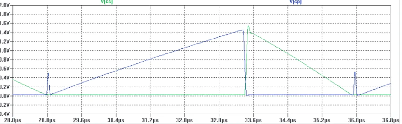
While not directly a loss in the transformer, the transformer has a significant amount of capacitance between the windings and between the opposing ends of the primary and secondary windings. In continuous mode, this capacitance energy is dissipated across the switch when it turns on during every switching cycle. In boundary mode, the energy is transferred to the magnetizing inductance of the transformer, but during this transfer a portion of the energy is lost. The only way to determine the amount of energy in this capacitance is by observing a flyback capacitor charger in opera-tion. In discontinuous mode, the capacitance forms a second-order network with the magnetizing inductance and rings. By measuring the frequency and the magnetizing inductance, the total capacitance on the switch pin can be calculated. This total capacitance not only accounts for all the parasitic capacitance in the transformer, but also the diode’s capacitance and the switch’s capacitance. The formula to calcu-late the total parasitic capacitance is shown below along with a scope photo of the fall-time, Figure 3-6. Cpara = (4ttf) 2 4π2L pri (3.11) In the equation, ttf is the fall-time of the flyback waveform. It is also measured
in the scope photo, Figure 3-6.
3.4
Diode Losses
While the diode is in forward conduction, the power loss is approximately the forward voltage drop times the current. In the case of a flyback capacitor charger, the current through the diode cannot be approximated as constant. The power equation needs to be integrated over a switching cycle and divided by the time period of a switching cycle. This results in the following equation.
Pdiode = VfIlim(1 + α)
Vin+ Vout
2Vout(Vout+ NVin)
The forward diode drop does not contribute a significant loss above 25V.
Another loss occurs in the diode when it turns off. The diode stores a small amount of charge when conducting forward current. The diode conducts current in the opposite direction to remove this charge. The amount of time it takes is called the reverse recovery time. Modern diodes that only conduct small amounts of current typically have very fast reverse recovery times. The reverse recovery current is proportional to the forward current of the diode at turn off. In the diode used in the test circuit, a Vishay GSD2004S, the reverse recovery time (trr) is 50nS and the
reverse recovery current is 3mA with a 30mA forward current prior to the turn off. By using a very conservative estimation using the following equation to calculate the
Figure 3-6: Scope shot: Ch4 is primary switch pin.
power loss, VoutIFtrrf , the reverse recovery loss is not significant compared to the
other losses and will not be modeled.
3.5
Charge time
There are many different approaches to calculate charge time. To start with the simplest method, the input current over the charge cycle can be approximated as constant. This is a fairly accurate representation in the test circuit above 100V. With this one assumption, the charge time can be found with the following equation.
tcharge =
CloadVout2
IinVinµ
(3.13) In the equation above, µ is the total efficiency of the circuit. This model of the charge time is relatively simple and is not that useful, except to understand on a first order how parameters influence charge time.
A more complete model is derived by integrating ∆t
∆v over the charging voltage
range. Instructions on how to calculate ∆t
∆v are in Chapter 4, Modeling in MATLAB.
This integration results in the following equation.
tcharge = Z Vout 0 ∆t ∆vdv = CVout Ilimµ (Vout Vin + 2N) 1 − α 1 − α2 (3.14)
This equation shows the effects of changing α and the other parameters. With an
α close to 1, the charge time decreases by half over an α of 0.
The last two methods have assumed a constant efficiency over the charge cycle. The efficiency varies by up to 10% over the charge cycle, so the previous methods would be inaccurate. While this can be done numerically with an efficiency plot, there are no benefits because charge time cannot be modeled to this accuracy because of circuit delays. There are two major delays not accounted for in the models above. The first major delay is the amount of time it takes for the primary winding current to decrease, and transfer to the secondary winding. Another delay is the amount of time it takes for the switch to turn back on. These delays will be explained in more
Chapter 4
Modeling in MATLAB
4.1
Introduction
This thesis uses MATLAB to numerically calculate the losses for a flyback capacitor charger. The vector operations are used extensively, along with the analytical expres-sions in Chapter 3, to calculate the losses. These vectors are capable of calculating these loss equations over the range of Vout.
4.2
Calculating Individual Losses
The first step in developing a model to evaluate the performance of a flyback capacitor charger is to plot each of the individual loss term versus output voltage. These individual losses are shown in Figure 4-1 and Figure 4-2. Each of these individual loss terms are checked for obvious errors. A high power loss in any of these terms generates heat, which is easy to check for in lab. The two major loss terms correspond with the two components which become warm during operation, therefore assuring reasonable values for each of the individual power losses.
Each of the losses needs the correct behavior over output voltage range. There are four different types behavior over Vout out of the nine loss terms. The primary
winding resistance (Pdcp), the switch resistance (Psw), and the leakage inductance (Pleak) increase with the duty cycle of flyback capacitor charger. The duty cycle, or
the proportion of time the switch is on, increases quickly at lower voltages and stays relatively constant over 100V. The diode loss (Pdiode), and the secondary winding loss (Pdcs) are proportional to current through the secondary winding. The average current through the secondary side of the circuit is proportional to the complement of the duty cycle, and determines the loss in these two secondary side components. The loss due to the parasitic capacitance of the transformer increases quadratically with Vout, because the energy stored in this capacitance is proportional to Vout2 . The
rise and fall time losses from the switch are proportional to the operating frequency. The core loss is proportional to frequency to 1.72 power with the TDK core.
0 50 100 150 200 250 300 0 0.02 0.04 0.06 0.08 0.1 0.12 0.14 0.16 0.18 0.2 Output Voltage (V) Power of Loss (W)
Breakdown of Losses from a Typical Flyback Charger (Part 1 of 2)
Pdcp Pdcs Pleak Psw
Figure 4-1: Breakdown of losses from a typical flyback charger (Part 1 of 2). Subtracting the sum of all these losses from the input power calculates the output power. Efficiency simply equals Pout
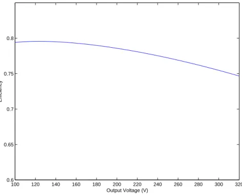
Pin; a plot of efficiency is generated, as shown in
Figure 4-3. This plot shows the decrease in efficiency at higher output voltages caused mainly by the losses due to parasitic capacitances on the switch. At higher output voltages, the operating frequency increases. Consequently, the frequency-dependent losses increase at higher output voltages. The parasitic capacitance loss
increases quadratically with output voltage and is the main cause of efficiency decrease at higher output voltages. The plot shown in Figure 4-3 is relatively flat because of adequate magnetizing inductance, keeping operating frequency low. Operating frequency should be kept low enough to keep the parasitic capacitance from being the dominant loss term over the DC losses in the switch and the primary winding.
To plot efficiency versus a parameter such as magnetizing inductance, we need to convert the efficiency plot into total efficiency. The efficiency curve is deceiving since the charger spends more time at higher voltages. By starting with power loss in terms of Vout, we can multiply this with ∆V∆t. The first step in calculating dVdt is to find the
output voltage increase per switching cycle as a function of the output voltage. The amount of energy added to the output capacitor each cycle is the energy held in the magnetizing inductance. This leads to the following equation.
1 2LpI 2 lim(1 − α2) = 1 2C(V + ∆V ) 2 −1 2CV 2. (4.1)
By solving for ∆V and ignoring second-order terms, we arrive at the following
0 50 100 150 200 250 300 0 0.02 0.04 0.06 0.08 0.1 0.12 0.14 0.16 0.18 0.2 Output Voltage (V) Power of Loss (W)
Breakdown of Losses from a Typical Flyback Charger (Part 2 of 2)
Pdiode Pcloss Pf Pr Pcore
equation. ∆V = LpI 2 lim 2CoutVout . (4.2)
∆t is simply the reciprocal of the the cycle frequency, or ton+ tof f. By dividing
these two terms, we arrive at ∆t ∆V = 2CVout Ilim 1 − α 1 − α2[ 1 Vin− Vsat + N Vout+ Vd ]. (4.3) After multiplying the power loss curve with (4.3), we integrate over this new curve, giving us the energy lost during a charge. An integral is impossible to do with sampled data, so the integral is approximated by summing the multiplication of the value of the efficiency by the distance between efficiency data points for all the efficiency data points. The total efficiency is given by energy out divided by the energy in. The energy out is equal to the energy stored in the capacitor, 1
2CV2 and the energy in is
given by the energy out plus the energy lost in charging. By creating a MATLAB function with this as an output, we may plot efficiency as parameters are changed.
100 120 140 160 180 200 220 240 260 280 300 320 0.6 0.65 0.7 0.75 0.8 Efficiency Output Voltage (V)
Table 4.1 lists all the inputs to this function and a short description, while the code is listed in Appendix A.
Variable Name Description
Al Henries per turns squared Wa Winding Window Area MLT Mean Length per Turn Ve Effective Volume of Core
Ae Effective Cross-sectional Area of Core
Bex βValue in Core Power Loss Equation
fex ξ Value in Core Power Loss Equation
n Number of Turns for Primary Winding N Turns ratio
Iin Average Input Current
alpha Sets Secondary Current Limit Cload Load Capacitance
Vin Input Voltage
Vmax Final Output Voltage
leakpercent Leakage Inductance is this Fraction of Magnetizing Inductance primarywinding Fraction of Winding Window Dedicated to Primary Winding
Table 4.1: Table of inputs to total efficiency function for flyback charger. As an example, Figure 4-4 shows a sweep of magnetizing inductance for a typical flyback capacitor charger. Each inductance uses the same core and winding window area. As the the inductance increases, the number of turns on both the primary and secondary windings increases, so therefore the cross-section area of the wire needs to be smaller to fit within the allocated winding window. The function accounts for this new cross-sectional area by calculating the resistance per length of the wire and multiplying by the required length of the winding based on the mean length per turn information given by the core manufacturer.
0 0.5 1 1.5 2 2.5 3 3.5 4 x 10⁻⁵ 0.66 0.68 0.7 0.72 0.74 0.76 0.78 0.8
Efficiency Vs. Magnetizing Inductance
Magnetizing Inductance (L)
Efficiency
Chapter 5
Design, Construction and Testing
of a Flyback Capacitor Charger
5.1
Introduction
Designing a flyback capacitor charger controller is straightforward. Without the com-plicated feedback loops of regulating DC/DC converters, the flyback capacitor charger is driven by three main events. The design of a flyback controller can be done by hand initially and requires no equations. The controller to be built will operate with a variable frequency, the advantages of this are discussed in a previous section, and the basic operation is as follows. The primary current needs to be monitored and once an adjustable current limit is met, the switch turns off. Then, as the secondary cur-rent feeds the output capacitor, the curcur-rent decreases to the secondary curcur-rent limit, and the switch turns back on. The output voltage needs to monitored to check if an adjustable final output voltage has been reached. With the two adjustable current limits, any α is possible while keeping the average input current constant.
5.2
Design
Most of the controller circuitry is digital, except the portion that determines the current in the primary and secondary windings. To determine the current on the
Vin 680 F + 4.7 F -T1 D1 Cout Photoflash Capacitor + -Vcc 1K 5K + -U1.1 U2.1 Vsec U5 U6.1 D2 +U3.2 -40K 70K 250K 262K Vin Vin 2 + U1.2 -Vcc 1K + U3.1 -Vs R2 R1 In Out Vcc U4 Si230805 U7.1 S R Q Q + -Vcc U2.2 DC U7.2 S R Q Q D3 U6.2 ENABLE U5.3 U5.2 U8.2 U1: LT1801CS8 U2,U3: LT1720CS8 U4: LTC1693-1CS8 U5: 74LS00 U6: 74LS04 U7: 74LS08 U8: 74LS163 T1: TDK EPC10 core
D1: Vishay GSD2004S Dual Diode Connect in series D2,D3,D4:Zetex ZHCS400 C1: 4.7 F, X5R or X7R, 10V U8.1 D4 0:Continuous Mode 1:Boundary Mode 0 1 C1 1K 1K 200pF 200pF
primary, a low-value sense resistor is placed between ground and the source of the MOSFET. A non-inverting operation amplifier configuration is used to measure the current across the sense resistor. This amplified version of the sense resistor voltage is compared with the adjustable primary current limit reference voltage with a com-parator. When the current reaches the current limit, the comparator outputs high. Similarly, the voltage on the secondary winding is measured with a sense resistor between the the secondary winding and ground. The current on the secondary wind-ing is in the opposite direction, requirwind-ing the use of an invertwind-ing operation amplifier configuration. A comparator compares the output of the op amp with the secondary current limit voltage, so that the output goes high when the secondary current is less than the current limit.
After the primary and secondary currents are in digital form and are ready to be interfaced to the digital portion of the circuit. The digital portion of the circuit consists of one-shots, S-R latches, AND gates, and OR gates. The whole circuit, in Figure 5-1, is relatively simple in its operation with one exception. Once the controller is started with a rising edge on the net labelled ”ENABLE”, the switch turns on and the primary current in the transformer ramps up. The primary current will eventually trigger the primary current limit comparator and reset a latch. The output of the latch will then force the switch off. The comparator is connected to the latch through an AND gate, which has the other input connected to an inverted one-shot that triggers when the switch turns on. A current spike occurs after the switch turns on caused by the stray capacitance on the switch node. The one-shot disables the primary current comparator to turn the switch off. When the switch turns off, the energy stored in the core releases into the output capacitor. The secondary current declines to the secondary current limit and the comparator goes high, and this positive edge on the comparator signal triggers a one-shot. The one-shot turns on the latch that determines the state of the switch. At the beginning of the charge, a latch is set to tell the circuit to charge. When the final output voltage is reached, this latch turns off. This latch’s output is connected to an AND gate with the latch that determines the state of the switch. The circuit uses the reflected output voltage
on the primary winding during the flyback time period to determine if the capacitor is charged.
Figure 5-2: Simulated primary and secondary currents of test circuit.
We use LT1800s for the operational amplifier and we use LT1720s for the com-parators. The op amp was chosen since it has an acceptable slew rate. The one-shot is made by using an inverter and an AND gate, shown in Figure 5-1. The one-shot connected to the enable pin does not require a specific time length. However, the one used after the switch turns on, needs to have a duration long enough to blank the stray capacitor current, around 100nS. The S-R latches are J-K Flip-flops with preset and reset. The clock and the J-K inputs are tied to ground and only the preset and reset inputs are used. A LTC1693, a CMOS gate drive, is used to drive the MOSFET. After designing the flyback controller on paper, it was tested in Spice. One major error was found in the paper design. A one-shot after the secondary current com-parator was necessary. Although the magnetizing current will always remain above the secondary current limit, the secondary current drops to zero during the switch on period, therefore the secondary comparator output is high. When the primary current limit is reached, both inputs of the S-R latch are high, which is an undefined state. A rising edge event from the secondary output comparator is unique to the secondary current crossing the current limit from a higher current. A one-shot is the ideal circuit to capture this rising edge and turn the switch on. After finding this error, the circuit simulated in Spice as expected. The one-shot used in blanking the initial primary current was combined with this new one shot, since they fired at the same time.
5.3
Construction
While Spice simulations are useful for debugging purposes, actual testing in lab is necessary to make real performance measurements. Since most of the components are only available in surface mount packages, layout software was utilized to expedite routing of the copper board in-house. Constructing the board consists of determining the component packages, figuring out special requirements for traces, and paying attention to large switching current paths. The backside of the copper board is the ground plane. Many of the digital interconnects, required external wiring. A bypass capacitor was added near each of the voltage pins of the digital and analog parts used in the design.
When the board layout was complete, a routing machine was used to make the board. This process proceeded smoothly. To put the final touches on the board, the excess copper was removed with a soldering iron and tweezers. First, the digital logic for the one-shots were placed on the board. Because these were designed from scratch extensive tests were done to verify their performance. A major problem was detected with the first design, as shown in Figure 5-1 without the included diode. The one-shot needs a time in the low state to reset. The short off-time of the switch does not allow the one-shot to reset, so the design was modified with a diode to quickly charge the capacitor to its high state. After completion of the one-shots, the rest of the digital logic was connected. The next step was to place the analog components. This portion was straight forward and there was no easy way to test their individual functionality. After all components were properly assembled, the circuit was probed. The output of the op amps were probed to show the primary and secondary currents. Nothing worked on the first attempt. A couple of wiring errors were then found by reexamining the circuit. After fixing these errors, the circuit charged the capacitor.
5.4
Debugging
Further testing with a load to operate the flyback with a steady state output voltage. The circuit would operate initially, but then the output voltage would collapse. After a careful inspection of voltages at the time of the collapse, the collapse was linked to noise in the primary and secondary current sensing circuitry. The adjustable voltage levels for the current limits picked up noise from external sources and would cause the comparator to change states. A premature trigger of the primary current limit and a high α allows the circuit to enter an invalid state where the secondary current never exceeds the secondary current limit, thus not triggering the one-shot to turn the switch back on. A quick solution to the problem was to add more capacitance to the voltage limit inputs of the comparators and minimize the length of the wires feeding into these inputs.
5.5
Boundary Mode Operation
After studying the possible benefits of boundary mode operation, a circuit was added to allow the controller to operate in boundary mode. Instead of turning the switch on when the secondary current falls below the limit, the switch monitors when the switch pin falls below Vin. The ringing settles at Vin. At low voltages, the amplitude
of the ring is small, and the switch pin voltage falls slightly below Vin. To add a noise
margin, the comparator trips at a voltage slightly above Vin to guarantee the switch
turns on, but below the lowest possible flyback period voltage. The circuit is shown in Figure 5-3. The resistive dividers move the comparator trip point slightly above
Vin. They also lower the inputs to the comparator to keep it within its common-mode
range. The diode also protects the comparator by limiting the voltage seen at the input of the comparator to a diode drop above Vin. The one-shot is already present
in the existing circuitry. The secondary current comparator usually connects to the input of the one-shot. This input can be switched back and forth to change the circuit from boundary mode operation to continuous operation.
5.6
Final Product
The output of the flyback capacitor charger is shown in Figure 5-4. The input current waveform is filtered with a large bypass capacitor to show the average input current. The average input current stays constant over the charge cycle in this example using a 16uH magnetizing inductance, an output capacitance of 150uF and an input voltage of 3.5V. The output voltage increases as the square root of the time elapsed, since the energy input is constant and energy storage in a capacitor is proportional to voltage squared.
The final constructed circuit uses two separate power supplies. One power supply is for the digital logic, the gate driver, comparators, and the operational amplifiers and the other is for the energy to be transferred to the capacitor. The general architecture of the circuit makes it capable of accepting any input voltage, but low voltages suffer from high losses in efficiency. The maximum input voltage is set at 10V by the ceramic input capacitor, but could easily accommodate higher voltages. The MOSFET is rated at 2A with a breakdown voltage of 60V. This MOSFET allows the primary
Sw
Vin
Vin
1-Shot
-+
40k
250k
262k
40k
current limit to be as high as 2A and the output voltage to reach 600V with 10 turn transformer. With a low leakage inductance transformer, the α may be set as high as 0.9. The maximum input power is 16W with an input voltage of 10V, current limit of 2A, and an α of .9. But running at this power for an extended period of time would need adequate heat sinking. The charge time for this circuit follows equation 5.1. The plot in Figure 5-4 shows a charge time of 6.7s. The equation predicts a charge time of 7.2s. The charge time is slightly higher due to dielectric absorbtion in the capacitor, lowering the value of the capacitance with a quick charge. Experimental charge times predict other charge times with different photoflash capacitance values nicely by scaling.
tcharge =
CloadVout2
IinVinµ
(5.1)
Chapter 6
Transformer Optimization
6.1
Introduction
This chapter focuses on the transformer and its impact on the performance of a flyback capacitor charger. A brief outline of the requirements of the transformer is presented in the first section. Within these requirements, the design still remains flexible. In the model developed to simulate the capacitor charger, the winding resistances and core loss are modeled. There is no easy way to model some of the parasitic effects of the transformer such as leakage inductance, winding capacitance, and proximity loss. The tradeoffs of these parameters are discussed without the use of simulations.
6.2
Transformer Basics
As discussed before in previous sections, the transformer serves a dual role in a flyback capacitor charger. The transformer protects the switch from the high output voltage, and it stores energy in the core. While the transformer is the simplest component to manufacture in a flyback, the transformer has the largest impact on efficiency. In addition, a transformer is also the largest component in a flyback capacitor charger. Therefore, the transformer is the most important component to optimize and analyze in depth.
winding is connected to the switch on the input side. The secondary winding is connected to the output capacitor through a diode. To protect the switch from high collector-to-emitter voltages, the secondary winding usually needs ten times the amount of turns as the primary winding in typical photoflash applications. In contrast with a forward converter, the flyback converter intentionally stores energy in the transformer’s magnetizing inductance. In most transformers, the magnetizing inductance is made as high as possible using an un-gapped core. A flyback converter uses a gapped-core transformer with energy stored as a magnetic field in the air gap. The amount of magnetizing inductance in the core is most important to the operation of the flyback converter because it determines the operating frequency of the flyback capacitor charger along with the primary and secondary current limits. The magnetizing inductance can be measured with an impedance analyzer on the primary and secondary windings, but this measurement includes the leakage inductance. The approximate turns ratio is found by taking the square root of the ratio of these two inductances. When the flyback waveform is used to determine when the output has reached its final value, the switch off portion needs to be long enough for a speed-limited comparator to trigger once the output voltage is reached. A minimum off-time will be specified by the controller, and this corresponds to a minimum secondary magnetizing inductance.
In an inductor, the winding is wrapped around the core as closely as possible to keep the flux in the core. But the core’s permeability is only several orders of magnitude larger than air so some flux is leaked into the surrounding air. When this happens in a transformer, the flux leaked into the air creates an inductance in series with the transformer, as shown in Figure 6-1. Leakage inductance is the worst when the primary and secondary windings are poorly coupled. Poor coupling occurs when flux from one winding has significant room to go between itself and the other winding. Coupling becomes worse with a winding area with a small width, since it leads to the use of many layers. These layers create a lot of space between the primary and secondary windings. A winding window with a large width is best to lower the amount of layers, thus decreasing leakage inductance. To improve leakage inductance, the
primary and secondary may be interleaved. It is typically possible to decrease leakage inductance by half with interleaving. In the flyback capacitor charger, multiple wires may be used for the primary winding and each of these windings could be interleaved with the secondary winding. This technique is difficult to do by hand for prototypes and is best left to transformer manufacturers.
While interleaving will reduce leakage inductance, it will increase the capacitance between the windings. This capacitance will increase the total lumped capacitance from the switch node and the secondary winding node, which can be analyzed as a reflected capacitance on the primary switch node. In continuous operation mode, the capacitance on the switch node is charged to the transformer’s step-downed output voltage when the switch turns on. This capacitance discharges through the closed switch. At lower output voltages, the amount of energy lost is low, but it increases with the square of the output voltage, and becomes the dominate loss term at higher voltages.
The capacitance between the windings is distributed throughout both of the wind-ings and cannot be well modeled with a lumped capacitance linking the two windwind-ings. If the secondary winding is put on top of the primary winding, the capacitance is greater on the section of the winding directly on top of the primary winding. This pin of the secondary winding should be connected to ground to minimize the effect of the interwinding capacitance. In experiments, the efficiency decreases by at least 5% if the preferential transformer connection is not used.
Losses in the core and the windings are discussed in Chapter 3. The primary winding DC resistance loss is the greatest out of these losses. The duty cycle of the charger is relatively constant above 100V where is spends most of its time. Therefore, the amount of power lost in the primary and secondary windings is constant over the charge cycle. While decreasing the primary winding resistance helps efficiency, its returns are marginal because the switch’s on-resistance is in series with the winding and is usually much higher in a well-designed transformer. In addition, a larger gauge primary winding increases the leakage inductance.