HAL Id: tel-00351338
https://tel.archives-ouvertes.fr/tel-00351338
Submitted on 9 Jan 2009HAL is a multi-disciplinary open access archive for the deposit and dissemination of
sci-L’archive ouverte pluridisciplinaire HAL, est destinée au dépôt et à la diffusion de documents
Techniques d’impression et matériaux semiconducteurs
pour l’électronique plastique
Etienne Menard
To cite this version:
Etienne Menard. Techniques d’impression et matériaux semiconducteurs pour l’électronique plastique. Matière Condensée [cond-mat]. Université Pierre et Marie Curie - Paris VI, 2005. Français. �tel-00351338�
THESE DE DOCTORAT DE L’UNIVERSITE PARIS 6
Spécialité :
Chimie Moléculaire
Présentée par
Etienne MENARD
Ingénieur ENSEEIHT
pour obtenir le grade de
Docteur de l’Université Paris VI
Techniques d’impression et materiaux semiconducteurs pour
l’électronique plastique
-Stamping Techniques and Semiconducting Materials for
Plastic Electronics
Soutenue le 18 octobre 2005 devant la commission d’examen composée de :
Dr Denis FICHOU
Directeur de thèse
Pr John A. ROGERS
Codirecteur de thèse
Pr Max MALACRIA
Président du jury
Dr Lhadi MERHARI
Rapporteur
Dr Jean RONCALI
Rapporteur
Thèse préparée au:
CEA Saclay, LRC Nanostructures et Semi-Conducteurs Organiques CNRS-CEA-UPMC
&
Beckman Institute for Advanced Science and Technology Seitz Materials Research Laboratory
Department of Materials Science and Engineering University of Illinois at Urbana-Champaign
Contents
Page
1 Introduction 1
I
Stamping Techniques for Micro and Nanofabrication
3
2 Overview of Stamping Techniques: Methods and Applications 5
2.1 Introduction . . . 5
2.2 High Resolution Stamps . . . 6
2.3 Microcontact Printing . . . 9
2.4 2D and 3D Dimensional Nanofabrication with Conformable Photomasks . . . . 13
2.5 Nanotransfer Printing . . . 16
2.6 Applications: Unconventional Electronic Systems . . . 21
2.7 Conclusions . . . 29
3 Improved Surface Chemistries, Thin Film Deposition Techniques and Stamp De-signs for Nanotransfer Printing 31 3.1 Introduction . . . 31
3.2 Surface Chemistry and Thin Film Deposition Effects on Nanotransfer Printing. 33 3.3 Two and Three Dimensional Printing Using Optimized Stamp Relief Profiles. . 37
3.4 Tough, Flexible Stamps that Use Thin Polymer Backings. . . 40
3.5 Conclusions . . . 42
3.6 Experimental Section . . . 43
3.6.1 Fabrication of Stamps with Re-Entrant Sidewalls . . . 44
3.6.2 Fabrication of Stamps with Flexible Polymer Backings . . . 44
3.6.3 Instrumentation . . . 45
4 Dry Transfer Printing Techniques with High Resolution Molded Rubber Stamps 47 4.1 Deposition and Patterning of High-Performance Semiconductors on Flexible Substrates . . . 47
iv CONTENTS
4.2 Dry Transfer Printing of Inorganic Semiconductor Micro-Structures and Carbon
Nanotubes . . . 48
4.3 Conclusion and Future Outlook . . . 53
4.4 Experimental Section: Dry Transfer Printing ofµs-Si Devices . . . 53
II
Organic Semiconductors
55
5 Overview of Organic Semiconductor Devices 59 5.1 From Conducting Polymers to Organic Single Crystal Semiconductors . . . 595.2 Organic Single Crystal Growth . . . 61
5.3 Field Effect Transistor Devices . . . 64
5.3.1 Electrostatic Bonding Technique . . . 64
5.3.2 Parylene Dielectric . . . 65
6 Reversible Probing of Charge Transport in Organic Crystals 67 6.1 The Soft ‘Transistor Stamp’ for Probing Organic Single Crystals . . . 68
6.2 Charge Transport in a Rubrene Single Crystal . . . 70
6.3 Anisotropy of the Charge Transport at the Basal Plane of a Rubrene Single Crystal 72 6.4 Experimental section . . . 74
6.4.1 Materials and Methods: . . . 74
6.4.2 Transistor Characterization: . . . 74
7 ‘Air-Gap’ Stamps 77 7.1 Background: Need for a New Test Structure . . . 77
7.2 The ‘Air-Gap’ Stamp . . . 78
7.2.1 Fabrication of the Air-Gap Stamp . . . 78
7.2.2 Characterization of the Stamp Electro-Mechanical Properties . . . 79
7.3 TCNQ and Rubrene Field Effect Transistor Devices . . . 82
7.3.1 Single Crystal TCNQ Devices . . . 82
7.3.2 Single Crystal Rubrene Devices . . . 84
7.4 Conclusion . . . 86
7.5 Experimental Section: . . . 87
7.5.1 Building the Transistors: . . . 87
7.5.2 Preparing the Masters: . . . 87
7.5.3 Preparing the Stamps: . . . 87
8 Scanning Tunnelling Microscopy of a Rubrene Single Crystal 89 8.1 Surface and Bulk Analysis of a Semi-Conducting Organic Single Crystal . . . . 89
CONTENTS v 8.5 Conclusion . . . 95
9 Conclusion and perspectives 97
A Matlabr Code for Substracting Overall Translational and Rotational
Misalign-ments 113
A.1 MatlabrCode . . . 113
A.2 Typical Program Outputs . . . 124
B Adhesion and Collapse of Soft Elastomeric Stamps 127
C List of Written and Oral Communications 135
Chapter 1
Introduction
Nous vivons dans une société ou l’image est un important vecteur de communication. Au cours de l’histoire, l’homme n’a cessé d’améliorer les supports physiques permettant de projeter et de diffuser l’information contenue dans ces images. Les récents progrès de l’électronique ont per-mis de rendre ce moyen de communication plus vivant, réactif à la demande de l’observateur. De nombreux supports permettent aujourd’hui une réactualisation rapide du contenu visuel per-mettant ainsi une mise à jour constante de l’information véhiculée. Ces systèmes de projec-tion d’images font un usage intensif de matériaux semi-conducteurs dits “classiques” tel que le silicium mono-cristallin. En raison de leur inhérente fragilité, ces types de semi-conducteurs inorganiques ont des propriétés mécaniques qui se prêtent mieux à la fabrication de circuits sur substrats rigides ayant des propriétés chimiques compatible avec les procédés à haute tempéra-ture nécessaires à la production de systèmes optoélectroniques performants.
Pour permettre la fabrication de tels systèmes électroniques sur supports souple, de nou-veaux matériaux et techniques de fabrication doivent être inventés. Ces nouvelles méthodes ont pour ultime but la création d’une gamme nouvelle de dispositifs électroniques sur des sub-strats ayant des propriétés chimiques et mécaniques variées, pouvant entre autre être légers, flexibles et peu onéreux. Le développement de matériaux semi-conducteurs ayant des pro-priétés biochimiques adéquates permettra aussi d’ajouter des fonctionnalités inédites à ces systèmes électroniques “souples” qui sont aujourd’hui difficilement réalisables avec les tech-niques et matériaux couteux utilisés en micro-électronique conventionnelle. Ces recherches déboucheront dans un futur proche sur la commercialisation d’écrans souples avec des produits destinés au marché public par le biais de nombreux secteurs de diffusions tels que: la téléphonie, la télévision, la publicité, l’architecture, la mode. De plus, de nouvelles applications naîtront à la demande de l’industrie aéronautique, automobile, spatiale et de l’armée.
La première partie de ce travail de recherche concerne le développement de nouvelles tech-niques de fabrication qui permettront la fabrication, à bas coups, sur de grandes surfaces, de ces circuits électroniques souples. Nous verrons à travers de nombreux exemples de prototypes que
2 Introduction
ces nouvelles techniques représentent une alternative intéressante aux techniques de lithogra-phie “classiques” développées par l’industrie de la micro-électronique. La deuxième partie de cette thèse sera portée sur une étude plus “fondamentale” d’un semi-conducteur organique ayant des propriétés électroniques très prometteuses : le rubrene. Par le biais de nouvelles méth-odes de fabrication, que nous avons spécifiquement développées pour tester ce matériau à l’état cristallin, nous verrons comment nous avons réussi à enrichir les connaissances scientifiques relatives aux phénomènes de transport de porteurs dans les matériaux organiques.
Le corps de ce document est rédigé en anglais afin de permettre une meilleure diffusion de ces résultats de recherche.
Part I
Stamping Techniques for Micro and
Nanofabrication
Chapter 2
Overview of Stamping Techniques:
Methods and Applications
2.1
Introduction
There is considerable interest in methods for building structures that have micron or nanome-ter dimensions. Historically, research and development in this area has been driven mainly by the needs of the microelectronics industry. The spectacularly successful techniques that have emerged from those efforts – photolithography, electron beam lithography, etc. – are extremely well suited to the tasks for which they were principally designed: forming structures of radi-ation sensitive materials (e.g. photoresists or electron beam resists) on ultraflat glass or semi-conductor surfaces. Significant challenges exist in adapting these methods for new emerging applications and areas of research which require patterning of unusual systems and materials (e.g. those in biotechnology, plastic electronics, etc.), structures with nanometer dimensions (i.e. below 50-100 nm), large areas in a single step (i.e. larger than a few square centimeters) or non-planar (i.e. rough or curved) surfaces. These established techniques also have the disad-vantage that they involve high capital and operational costs. As a result, some of the oldest and conceptually simplest forms of lithography – embossing, molding, stamping, writing, etc. – are now being re-examined for their potential to serve as the basis for nanofabrication techniques that can avoid these limitations.1 Considerable progress has been made in the last few years, mainly by combining these approaches or variants of them with new materials, chemistries and processing techniques. This chapter highlights some recent advances in high resolution printing methods, in which a ‘stamp’ forms a pattern of ‘ink’ on a surface that it contacts. It focuses on approaches whose capabilities, level of development and demonstrated applications indicate a strong potential for widespread use, especially in areas where conventional methods are unsuit-able.
Contact printing involves the use of an element with surface relief (i.e. the ‘stamp’ ) for transferring material applied to its surface (i.e. the ‘ink’ ) to locations on a substrate that it
6 Overview of Stamping Techniques: Methods and Applications
contacts. The printing press, which represents one of the earliest manufacturable implementa-tions of this approach, was due to Gutenberg and first appeared in the 15thcentury. The general approach has been since used almost exclusively for producing printed text or images with fea-tures that are one hundred microns or larger in their minimum dimension. The resolution is determined by the nature of the ink and its interaction with the stamp and/or substrate, the res-olution of the stamp, and the processing conditions that are used for printing or for converting the pattern of ink into a pattern of functional material. This chapter focuses on (i) printing tech-niques that are capable of micron and nanometer resolution and (ii) their use for fabricating key elements of active electronic or optical devices and subsystems. It begins with an overview of some methods for fabricating high resolution stamps. It then illustrates two different ways that these stamps can be used to print patterns of functional materials. Applications that highlight the capabilities of these techniques and the performance of systems that are constructed with them are also presented.
2.2
High Resolution Stamps
The printing process can be separated into two parts: fabrication of the stamp and the use of this stamp to pattern features defined by the relief on its surface. These two processes are typically quite different, although it is possible in some cases to use patterns generated by a stamp to produce a replica of that stamp. The structure from which the stamp is derived, which is known as the ‘master’, can be fabricated with any technique that is capable of producing well defined structures of relief on a surface. This ‘master’ can then be used directly as the stamp, or it can be used to produce stamps via molding or printing procedures. It is important to note that the technique for producing the ‘master’ does not need to be fast or low in cost. It also does not need to possess many other characteristics that might be desirable for a given patterning task: it is used just once to produce a ‘master’ which is directly or indirectly used to fabricate stamps. Each one of these stamps can then be used many times for printing. In a common approach for the high resolution techniques that are the focus of this chapter, an established lithographic technique, such as one of those developed for the microelectronics industry, defines the master. Figure 2.1 schematically illustrates typical processes.
Here, photolithography patterns a thin layer of resist on a silicon wafer. Stamps are gen-erated from this structure in one of two ways: by casting against this master or by etching the substrate with the patterned resist as a mask. In the first approach, the master itself can be used multiple times to produce many stamps, typically using a light or heat-curable prepolymer. In the second, the etched substrate serves as the stamp; additional stamps can be generated ei-ther by repeating the lithography and etching, or by using the original stamp to print replica stamps. For minimum lateral feature sizes greater than v1-2 microns, contact or proximity
2.2 High Resolution Stamps 7
Figure 2.1: Schematic illustration of two methods for producing high resolution stamps. The first
step involves patterning a thin layer of some radiation sensitive material, known as the resist, on a flat substrate, such as a silicon wafer. It is convenient to use an established technique, such as pho-tolithography or electron beam lithography, for this purpose. This structure, known as the ‘master’, is converted to a stamp either by etching or by molding. In the first case, the resist acts as a mask for etching the underlying substrate. Removing the resist yields a stamp. This structure can be used directly as a stamp to print patterns or to produce additional stamps. In the molding approach, a prepolymer is cast against the relief structure formed by the patterned resist on the substrate. Cur-ing (thermally or optically) and then peelCur-ing the resultCur-ing polymer away from the substrate yields a stamp. In this approach, many stamps can be made with a single ‘master’ and each stamp can be used many times.
convenient method to fabricate the master. For features smaller than v2 microns, several
dif-ferent techniques can be used,2 including: (i) projection mode photolithography,3 (ii) direct write electron beam (or focused ion beam) lithography,4, 5 (iii) scanning probe lithography6–9
or (iv) laser interference lithography.10 The first approach requires a photomask generated by
some other method, such as direct write photolithography or electron beam lithography. The reduction (typically 4x) provided by the projection optics relaxes the resolution requirements on the mask and enables features as small asv90 nm when deep ultraviolet radiation and phase
shifting masks are used. The costs for these systems are, however, very high and their availabil-ity for general research purposes is limited. The second method is flexible in the geometry of patterns that can be produced and the writing systems are highly developed: 30-50 nm features can be achieved with commercial systems,11 and < 10 nm features are possible with research tools, as first demonstrated more than 25 years ago by Broers et al.12 The main drawback of this
method is that it is relatively slow and it is difficult to pattern large areas. Like projection mode photolithography, it can be expensive. The third method, scanning probe lithography, is quite powerful in principle, but the tools are not as well established as those for other approaches. This technique has atomic resolution, but its writing speed can be lower and the areas that can be patterned are smaller than electron beam systems. Interference lithography provides a
8 Overview of Stamping Techniques: Methods and Applications
erful, low cost tool for generating periodic arrays of features with dimensions down to 100-200 nm; smaller sizes demand ultraviolet lasers and patterns with aperiodic or non-regular features are difficult to produce.
Figure 2.2: Schematically illustrates a process for examining the ultimate limits in resolution of soft
lithographic methods. The approach uses a SWNT master to create a PDMS mold with nanoscale relief features. Soft nanoimprint lithography transfers the relief on the PDMS to that on the surface of an ultraviolet curable photopolymer film.
In order to evaluate the ultimate resolution limit of the soft lithography methods, masters having relief structures in the single nanometer range must be fabricated. A simple method, pre-sented in figure 2.2, uses a sub-monolayer coverage of single walled carbon nanotubes (SWNT) grown, by established chemical vapor deposition techniques, on an ultra flat silicon wafer. The SWNT, which have diameters (i.e. heights and widths) in the 0.5-5 nm range, are molded on the bottom surface of a PDMS stamp generated by casting and curing against this master. Such a mold can be used to replicate the relief structure into a variety of photocurable polymers in a kind of soft nanoimprinting technique.13–15 A single mold can be used multiple times without
significant degradation. The resolution of this process can be exceedingly high: resolution ap-proaching the single nanometer scale range (comparable to a few bond lengths in the polymer backbone) as can be seen in figure 2.3.16 These results demonstrate extreme efficiency of these
2.3 Microcontact Printing 9
Figure 2.3: Atomic force micrographs (left picture) of a ‘master’ that consists of a sub-monolayer
of single walled carbon nanotubes (SWNTs; diameter between 0.5 and 5 nm) grown on a SiO2/Si
wafer. The right atomic force micrograph shows a replica of the relief structures in poly(urethane). These results indicate effective operation of a PDMS stamp for soft imprint lithography at the single nanometer scale.
2.3
Microcontact Printing
Microcontact printing (µCP)17 is one of several soft lithographic techniques – replica
mold-ing, micromolding in capillaries, microtransfer moldmold-ing, near-field conformal photolithography using an elastomeric phase-shifting mask, etc. – that have been developed as alternatives to established methods for micro- and nanofabrication.18–22 µCP use an elastomeric element
(usu-ally polydimethylsiloxane – PDMS) with high resolution features of relief as a stamp to print patterns of chemical inks. It was mainly developed for use with inks that form self-assembled monolayers (SAMs) of alkanethiolates on gold and silver. The procedure for carrying outµCP
in these systems is remarkably simple: a stamp, inked with a solution of alkanethiol, is brought into contact with the surface of a substrate to transfer ink molecules to regions where the stamp and substrate contact. The resolution and effectiveness of µCP relies on conformal contact
between the stamp and the surface of the substrate, rapid formation of highly ordered monolay-ers,23 and autophobicity of the SAM, which effectively blocks the reactive spreading of the ink
across the surface.24 It can pattern SAMs over relatively large areas (vup to 0.25 ft2
have been demonstrated in prototype electronic devices) in a single impression.25 The edge resolution of
SAMs printed onto thermally evaporated gold films is on the order of 50 nm, as determined by lateral force microscopy.26 Microcontact printing has been used with a range of different SAMs on various substrates.18 Of these, alkanethiolates on gold, silver and palladium27presently give the highest resolution. In many cases, the mechanical properties of the stamp limit the sizes of
10 Overview of Stamping Techniques: Methods and Applications
Figure 2.4: Schematic illustration of microcontact printing. The first step involves ‘inking’ a
‘stamp’ with a solution of a material that is capable of forming a self assembled monolayer (SAM) on a substrate that will be printed. In the case illustrated here, the ink is a millimolar concentration of hexadecanethiol (HDT) in ethanol. Directly applying the ink to the surface of the stamp with a pipette prepares the stamp for printing. Blowing the surface of the stamp dry and contacting it to a substrate delivers the ink to areas where the stamp contacts the substrate. The substrate consists of a thin layer of Au on a flat support. Removing the stamp after a few seconds of contact leaves a patterned SAM of HDT on the surface of the Au film. The printed SAM can act as a resist for the aqueous based wet etching of the exposed regions of the Au. The resulting pattern of conducting gold that can be used to build devices of various types.
the smallest features that can be achieved: the most commonly used elastomer (Sylgard 184, Dow Corning) has a low modulus which can lead to mechanical collapse or sagging for features of relief with aspect ratios greater than v2 or less than v0.05. Stamps fabricated with high
modulus elastomers avoid some of these problems.28, 29 Conventional stamps also are
suscepti-ble to in-plane mechanical strains that can cause distortions in the printed patterns. Composite stamps that use thin elastomer layers on stiff supports are effective at minimizing this source of distortion.30 Methods for printing that avoid direct mechanical manipulation of the stamp can
reduce distortions with conventional and composite stamps.25 This approach has proven to be effective in large area flexible circuit applications that require accurate multilevel registration.
2.3 Microcontact Printing 11
Figure 2.5: Scanning electron micrographs of typical structures formed by microcontact printing
a self-assembled monolayer ink of hexadecanethiol onto a thin metal film followed by etching of the unprinted areas of the film. The left frame shows an array of Au (20 nm thick) dots withv500
nm diameters. The right frame shows a printed structure of Ag (100 nm thick) in the geometry of interdigitated source/drain electrodes for a transistor in a simple inverter circuit. The edge resolution of patterns that can be easily achieved with microcontact printing isv50-100 nm.
selective deposition to form structures of a variety of materials: metals, silicon, liquids, organic polymers, and even biological species. Figure 2.4 schematically illustrates the use ofµCP and
wet etching to pattern a thin film of Au. Figure 2.5 shows SEM images of nanostructures of gold (20 nm thick, thermally evaporated with a 2.5 nm layer of Ti as an adhesion promoter) and silver (v100 nm thick formed by electroless deposition using commercially available plating
baths)31that were fabricated using this approach. In the first and second examples, the ‘masters’ for the stamps consisted of photoresist patterned on silicon wafers with projection and contact mode photolithography respectively. Placing these masters in a dessicator forv1 h with a few
drops of tridecafluoro-1,1,2,2-tetrahydrooctyl-1-trichlorosilane forms a silane monolayer on the exposed native oxide of the silicon. This monolayer prevents adhesion of the master to PDMS (Sylgard 184) that is cast and cured from a 10:1 mixture of prepolymer and curing agent. Plac-ing a few drops of av1 mM solution of hexadecanethiol (HDT) in ethanol on the surface of
the stamps, and then blowing them dry with a stream of nitrogen prepares them for printing. Contacting the metal film for a few seconds with the stamp produces a patterned self-assembled monolayer (SAM) of HDT. An aqueous etchant (1 mM K4F e(CN)6, 10 mM K3F e(CN)6
and 0.1 MNa2S2O3) removes the unprinted regions of the silver.32 A similar solution (1 mM
K4F e(CN)6, 10 mMK3F e(CN)6, 1.0 M KOH and 0.1 MNa2S2O3) can be used for etching
the bare gold.33 The results of Figure 2.5 show that the roughness on the edges of the patterns isv50-100 nm. The resolution is determined by the grain size of the metal films, the isotropic
etching process, slight reactive spreading of the inks and edge disorder in the patterned SAMs. The structures of Figure 2.5 were formed on the flat surfaces of silicon wafers (left image) and glass slides (right image). An attractive feature of µCP and certain other contact printing
techniques is their ability to pattern features with high resolution on highly curved or rough surfaces.22, 34, 35 This type of patterning task is difficult or impossible to accomplish with
pho-tolithography due to its limited depth of focus and the difficulty in casting uniform films of photoresist on non-flat surfaces. Figure 2.6 shows, as an example, a straightforward approach
12 Overview of Stamping Techniques: Methods and Applications
Figure 2.6: Schematic illustration of a simple method to print lines on the surfaces of optical fibers.
Rolling a fiber over the inked stamp prints a pattern onto the fiber surface. Depending on the orien-tation of the fiber axis with the line stamp illustrated here, it is possible, in a single roorien-tation of the fiber, to produce a continuous microcoil, or arrays of bands or stripes.
for high resolution printing on the highly curved surfaces of optical fibers. Here, simply rolling the fiber over an inked stamp prints a pattern on the entire outer surface of the fiber. Simple staging systems allow alignment of features to the fiber axis; they also ensure registration of the pattern from one side of the fiber to the other.20
Figure 2.7: Optical micrographs of some three dimensional microstructures formed by microcontact
printing on curved surfaces. The top frame shows an array of 3 micron lines of Au (20 nm) / Ti (1.5 nm) printed onto the surface of an optical fiber. This type of structure can be used as an integrated photomask for producing mode-coupling gratings in the core of the fiber. The bottom frames show a free standing metallic microstructure formed by (i) microcontact printing and etching a thin (100 nm thick) film of Ag on the surface of a glass microcapillary tube, (ii) electroplating the Ag to increase its thickness (to tens of microns) and (iii) etching away the glass microcapillary with concentrated hydrofluoric acid. The structure shown here has the geometry and mechanical properties of an intravascular stent, which is a biomedical device commonly used in balloon angioplasty.
2.4 2D and 3D Dimensional Nanofabrication with Conformable Photomasks 13
Figure 2.7 shows 3 micron wide lines and spaces printed onto the surface of a single mode optical fiber (diameter 125µm). The bottom frame shows a free standing metallic structure with
the geometry and mechanical properties of an intravascular stent, which is a biomedical device that is commonly used in balloon angioplasty procedures. In this latter caseµCP followed by
electroplating generated the Ag microstructure on a sacrificial glass cylinder that was subse-quently etched away with concentrated hydrofluoric acid.36 Other examples of microcontact printing on non-flat surfaces (i.e. low cost plastic sheets and optical ridge waveguides) appear in the applications section of this chapter.
2.4
2D and 3D Dimensional Nanofabrication with Conformable
Photomasks
PDMS rubber stamps can be used as soft photomasks since they are transparent to ultraviolet (UV) light with wavelengths greater than 300 nm. A first method, known as near field phase shift lithography involves exposure of a thin (i.e. .micrometer) photoresist layer to UV light that passes through an elastomeric phase mask while the mask is in conformal contact with the resist.37, 38
Figure 2.8: Part (a) shows a schematic illustration of the procedures for laminating a PDMS stamp
on a relatively thin (. micrometer) photoresist and generating patterns with nanometer scale after
UV exposure. Part (b) shows the photoresist lines and dots patterned with one and two exposures, respectively. Part (c) shows dense photoresist lines and spaces formed when the stamp relief struc-ture periodicity is close to the wavelength of the UV light (v365 nm) used for exposure. In this
special case, the stamp acts as an amplitude mask and produces a pattern in photoresist that has a one to one correspondence with the relief features on the stamp.
Figure 2.8a schematically illustrates the method. This approach requires only a phase mask and a simple handheld UV lamp to generate structures with dimensions as small as 50 nm over
14 Overview of Stamping Techniques: Methods and Applications
large areas (limited by the size of the molded stamp).39 By carefully choosing the height of the
relief features in the master, a sharp minimum appears in the intensity of light at the step edges of relief (when the phase is modulated byπ). Developing away the exposed regions of the resist
(when a positive resist is used) yields line patterns at the edges of the relief features mask. Figure 2.8b shows high resolution scanning micrographs of narrow line and dot patterns ob-tained by one or two exposures in this manner.40 If the distance between the edges of the stamp
relief features is reduced to a value close to the light wavelength, the two nulls in the near field intensity of the light add together. The transparent stamp then can serve as a sub-wavelength amplitude type photomask such that patterns molded in the stamps are reproduced in the pho-toresist layer in a one to one correspondence. Figure 2.8c illustrates this capability with 300 nm lines and spaces in a photoresist layer generated with a stamp that has similar features of relief.
Figure 2.9: Schematic illustration of the process for fabricating 3D periodic nanostructures using
the pattern of intensity formed by passage of light through a PDMS phase mask with sub-wavelength features of relief. (i) The stamp is first brought into intimate contact with the surface of a substrate coated with a relatively thick (several micrometers) transparent layer of a photopolymer. (ii) A laser beam or a regular UV mercury lamp source exposes this polymer through the photomask. (iii) The mask is peeled away and the unexposed regions of the photopolymer are removed by a developing step to create 3D polymer nanostructures.
As light propagates away from the surfaces of masks of this type, the intensity varies with position not only in the plane of the mask but also perpendicular to it. In the case of a mask with a grating geometry, this phenomenon is known as the Talbot effect. With thick transparent photoresists, one can exploit this effect to generate complex three dimensional nanostructures.41
2.4 2D and 3D Dimensional Nanofabrication with Conformable Photomasks 15
exposure. The variation of the intensity can be accurately predicted using a coupled wave or finite element analysis.
Figure 2.10: Scanning electron micrographs of representative 3D structures generated using a soft
photomask element. The top left inset images show the computed intensity models obtained from the addition of the intensity of the diffracted light beams. The precise fit between the experimental results and the mathematical models is remarkable.
Figure 2.10 shows various high resolution scanning electron micrographs of complex three dimensional periodic structures generated using this method. Supercritical drying during the de-veloping step avoids the destructive effects of surface tension on these fragile structures. These fine 3D structures have been successfully incorporated into a variety of microfluidic systems for filtering, mixing and other applications.
16 Overview of Stamping Techniques: Methods and Applications
2.5
Nanotransfer Printing
Nanotransfer printing (nTP) is a more recent high resolution printing technique which uses surface chemistries as interfacial ‘glues’ and ‘release’ layers (rather than ‘inks’ as inµCP) to
control the transfer of solid material layers from relief features on a stamp to a substrate.42–44 This approach is purely additive (i.e. material is only deposited in locations where it is needed) and it can generate complex patterns of single or multiple layers of materials with nanometer resolution over large areas in a single process step. It does not suffer from surface diffusion or edge disorder in the patterned ‘inks’ ofµCP nor does it require post-printing etching or
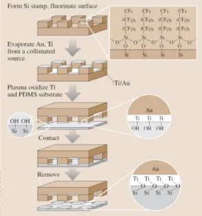
deposi-tion steps to produce structures of funcdeposi-tional materials. The method involves four components: (i) a stamp (rigid, flexible, or elastomeric) with relief features in the geometry of the desired pattern, (ii) a method for depositing a thin layer of solid material onto the raised features of this stamp, (iii) a means for bringing the stamp into intimate physical contact with a substrate and (iv) surface chemistries that prevent adhesion of the deposited material to the stamp and promote its strong adhesion to the substrate. nTP has been demonstrated with SAMs and other surface chemistries for printing onto flexible and rigid substrates with hard inorganic and soft polymer stamps. Figure 2.11 presents a set of procedures for using nTP to pattern a thin metal bilayer of Au/Ti with a surface transfer chemistry that relies on a dehydration reaction.42 The
process begins with fabrication of a suitable stamp. Elastomeric stamps can be built using the same casting and curing procedures described for µCP. Rigid stamps can be fabricated by (i)
patterning resist (e.g. electron beam resist or photoresist) on a substrate (e.g. Si or GaAs), (ii) etching the exposed regions of the substrate with an anisotropic reactive ion etch and (iii) removing the resist, as illustrated in Figure 2.1. For both types of stamps, careful control of the lithography and the etching steps yields features of relief with nearly vertical or slightly re-entrant sidewalls. The stamps typically have depths of relief > 0.2 µm for patterning metal
films with thicknesses < 50 nm.
Electron beam evaporation of Au (20 nm; 1 nm/s) and Ti (5 nm; 0.3 nm/s) generates uni-form metal bilayers on the surfaces of the stamp. A vertical, collimated flux of metal from the source ensures uniform deposition only on the raised and recessed regions of relief. The gold adheres poorly to the surfaces of stamps made of GaAs, PDMS, glass or Si. In the process of Figure 2.11, a fluorinated silane monolayer acts to reduce further the adhesion when a Si stamp (with native oxide) is used. The Ti layer serves two purposes: (i) it promotes adhesion between the Au layer and the substrate after pattern transfer, and (ii) it readily forms a v3 nm oxide
layer at ambient conditions which provides a surface where the dehydration reaction can take place. Exposing the titanium oxide (TiOx) surface to an oxygen plasma breaks bridging oxygen
bonds, thus creating defect sites where water molecules can adsorb. The result is a titanium oxide surface with some fractional coverage of hydroxyl (-OH) groups (titanol).
2.5 Nanotransfer Printing 17
Figure 2.11: Schematic illustration of nanotransfer printing procedures. Here, interfacial
dehydra-tion chemistries control the transfer of a thin metal film from a hard inorganic stamp to a conformable elastomeric substrate (thin film of polydimethylsiloxane (PDMS) on a plastic sheet). The process begins with fabrication of a silicon stamp (by conventional lithography and etching) followed by surface functionalization of the native oxide with a fluorinated silane monolayer. This layer en-sures poor adhesion between the stamp and a bilayer metal film (Au and Ti) deposited by electron beam evaporation. A collimated flux of metal oriented perpendicular to the surface of the stamp avoids deposition on the sidewalls of relief. Exposing the surface Ti layer to an oxygen plasma produces titanol groups. A similar exposure for the PDMS produces silanol groups. Contacting the metal coated stamp to the PDMS results in a dehydration reaction that links the metal to the PDMS. Removing the stamp leaves a pattern of metal in the geometry of the relief features.
plasma produces surface (-OH) groups (silanol). Placing the plasma oxidized, Au/Ti-coated stamp on top of these substrates leads to intimate, conformal contact between the raised regions of the stamp and the substrate, without the application of any external pressure. (The soft, con-formable PDMS is important in this regard.) It is likely that a dehydration reaction takes place at the (-OH)-bearing interfaces during contact; this reaction results in permanent Ti-O-Si bonds that produce strong adhesion between the two surfaces. Peeling the substrate and stamp apart transfers the Au/Ti bilayer from the raised regions of stamp (to which the metal has extremely poor adhesion) to the substrate. Complete pattern-transfer from an elastomeric stamp to a thin elastomeric substrate occurs readily at room temperature in open air with contact times of less than 15 seconds. When a rigid stamp is employed, slight heating is needed to induce transfer. While the origin of this difference is unclear, it may reflect the comparatively poor contact when rigid stamps are used; similar differences are also observed in cold welding of gold films.45
18 Overview of Stamping Techniques: Methods and Applications
Figure 2.12: Scanning electron micrograph (SEM) of a pattern produced by nanotransfer printing.
The structure consists of a bilayer of Au(20 nm)/Ti (1 nm) (white) in the geometry of a photonic bandgap waveguide printed onto a thin layer of polydimethylsiloxane on a sheet of plastic (black). Electron beam lithography and etching of a GaAs wafer produced the stamp that was used in this case. The transfer chemistry relied on condensation reactions between titanol groups on the surface of the Ti and silanol groups on the surface of the PDMS. The frames on the right show SEMs of the Au/Ti coated stamp (top) before printing and on the substrate (bottom) after printing. The electron beam lithography and etching used to fabricate the stamp limit the minimum feature size (v70 nm)
and the edge resolution (v5-10 nm) of this pattern.
Figure 2.12 shows scanning electron micrographs of a pattern produced using a GaAs stamp generated by electron beam lithography and etching. The frames on the right show images of the metal coated stamp before printing (top) and the transferred pattern (bottom). The resolution appears to be limited only by the resolution of the stamp itself, and perhaps by the grain size of the metal films. Although the accuracy in multilevel registration that is possible with nTP has not yet been quantified, its performance is likely similar to that of embossing techniques when rigid stamps are used.46
A wide range of surface chemistries can be used for the transfer. SAMs are particularly attractive due to their chemical flexibility. Figure 2.13 illustrates the use of a thiol termi-nated SAM and nTP for forming patterns of Au on a silicon wafer.43 Here, the vapor phase
co-condensation of the methoxy groups of molecules of 3-mercaptopropyltrimethoxysilane (MPTMS) with the -OH terminated surface of the wafer produces a SAM of MPTMS with exposed thiol (-SH) groups. PDMS stamps can be prepared for printing on this surface by coating them with a thin film (v15 nm) of Au using conditions (thermal evaporation 1.0 nm/s; v10−7 torr base pressure) that yield optically smooth, uniform films without the buckling that
has been observed in the past with similar systems.47 Nanocracking that sometimes occurs in
the films deposited in this way can be reduced or eliminated by evaporating a small amount of Ti onto the PDMS before Au deposition and/or by exposing the PDMS surface briefly to
2.5 Nanotransfer Printing 19
Figure 2.13: Schematic illustration of steps for nanotransfer printing a pattern of a thin layer of Au
onto a silicon wafer using a self-assembled monolayer (SAM) surface chemistry. Plasma oxidizing the surface of the wafer generates -OH groups. Solution or vapor phase exposure of the wafer to 3-mercaptopropyl-trimethoxysilane yields a SAM with exposed thiol groups. Contacting an Au-coated stamp to this surface produces thiol linkages that bond the gold to the substrate. Removing the stamp completes the transfer printing process.
the formation of sulfur-gold bonds in the regions of contact. Removing the stamp after a few seconds efficiently transfers the gold from the raised regions of the stamp (Au does not adhere to the PDMS) to the substrate. Covalent bonding of the SAM ‘glue’ to both the substrate and the gold leads to good adhesion of the printed patterns: they easily pass Scotch tape adhesion tests. Similar results can be obtained with other substrates containing surface -OH groups. For example, Au patterns can be printed ontov250µm thick sheets of poly(ethylene terephthalate)
(PET) by first spin casting and curing (130oC for 24 h) a thin film of an organosilsesquioxane on the PET. Exposing the cured film (v1µm thick) to an oxygen plasma then air produces the
necessary surface (-OH) groups.
Figure 2.14 shows some optical micrographs of typical printed patterns in this case.43 Sim-ilar surface chemistries can guide transfer to other substrates. Alkanedithiols, for example, are useful for printing Au onto GaAs wafers.44 Immersing these substrates (freshly etched with
37% HCl forv2 min. to remove the surface oxide) in a 0.05 M solution of 1,8-octanedithiol in
ethanol for 3 h produces a monolayer of dithiol on the surface. Although the chemistry of this system is not completely clear, it is generally believed that the thiol end groups chemically bond
20 Overview of Stamping Techniques: Methods and Applications
Figure 2.14: Optical micrographs of patterns of Au (15 nm thick) formed on plastic (left frame) and
silicon (right frame) substrates with nanotransfer printing. The transfer chemistries in both cases rely on self-assembled monolayers with exposed thiol groups. The minimum feature sizes and the edge resolution are both limited by the photolithography used to fabricate the stamps.
to the surface. Surface spectroscopy suggests the formation of Ga-S and As-S bonds. Contact-ing an Au-coated PDMS stamp with the treated substrate causes the exposed thiol endgroups to react with Au in the regions of contact. This reaction produces permanent Au-S bonds at the stamp/substrate interface (see insets in Figure 2.4 for idealized chemical reaction schemes).
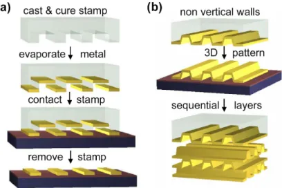
Figure 2.15: Schematic illustration of the nanotransfer printing (nTP) process for fabricating high
resolution 2D or 3D patterns of thin metals. Part (a) schematic schematically illustrates the process for generating 2D metal patterns. A metal coated stamp (formed using a collimated electron beam evaporator) is brought into intimate contact with the surface of a substrate. Chemical bonding or surface energy differences enable the transfer of the metal from the raised area of the stamp to the substrate. Part (b) illustrates schematically the process for generating continuous 3D structures when the stamp relief side walls are not vertical. Successive cold welding of gold films on top of each other yields complex multilayers structures.
2.6 Applications: Unconventional Electronic Systems 21
Figure 2.16: Scanning electron micrographs of three dimensional metal structures obtained by
nano-transfer printing gold metal films. Part (a) shows closed gold nano-capsules. Part (b) shows free-standing L structures obtained using a stamp coated with a steeply angled flux of metal. Part (c) shows a multilayer 3D structure obtained by the successive transfer and cold welding of continuous gold nano-corrugated films.
The integrity of the nanotransfer printed free standing 3D metal structures is remarkable (see Figure 2.16) but depends critically on the careful optimization of the metal evaporation conditions and stamp & substrate surface chemistries as we will see in the following chapter. Similar metal transfer techniques have been developed in other research groups.49, 50
2.6
Applications: Unconventional Electronic Systems
Although conventional patterning techniques, such as photolithography or electron beam lithog-raphy, have the required resolution, they are not appropriate because they are expensive and gen-erally require multiple processing steps with resists, solvents and developers that can be difficult to use with organic active materials and plastic substrates. Microcontact and nanotransfer print-ing are both particularly well suited for this application. They can be combined and matched with other techniques, such as ink jet or screen printing, to form a complete system for pat-terning all layers in practical plastic electronic devices.51 We have focused our efforts partly on
unusual electronic systems such as flexible plastic circuits and devices that rely on electrodes patterned on curved objects such as microcapillaries and optical fibers. We have also explored photonic systems such as distributed feedback structures for lasers and other integrated optical elements that demand sub-micron features. The sections below highlight several examples in each of these areas.
A relatively new direction in electronics research seeks to establish low cost plastic materi-als, substrates and printing techniques for large area flexible electronic devices, such as paper-like displays. These types of novel devices can complement those (e.g. high density memories,
22 Overview of Stamping Techniques: Methods and Applications
high speed microprocessors, etc.) that are well suited to existing inorganic (e.g. silicon) elec-tronics technologies. High resolution patterning methods for defining the separation between the source and drain electrodes (i.e. channel length) of transistors in these plastic circuits are particularly important because this dimension determines current output and other important characteristics.52
Figure 2.17: Schematic cross sectional view (left) and electrical performance (right) of an
or-ganic thin film transistor with microcontact printed source and drain electrodes. The structure con-sists of a substrate (PET), a gate electrode (indium tin oxide), a gate dielectric (spin cast layer of organosilsesquioxane), source and drain electrodes (20 nm Au and 1.5 nm Ti), and a layer of the organic semiconductor pentacene. The electrical properties of this device are comparable to or better than those that use pentacene with photolithographically defined source/drain electrodes and inorganic dielectrics, gates and substrates.
Figure 2.17 schematically illustrates a cross sectional view of a typical organic transis-tor. The frame on the right shows the electrical switching characteristics of a device that uses source/drain electrodes of Au patterned by µCP, a dielectric layer of an organosilsesquioxane,
a gate of indium tin oxide (ITO) and a PET substrate. The effective semiconductor mobility ex-tracted from these data is comparable to those measured in devices that use the same semicon-ductor (pentacene in this case) with inorganic substrates and dielectrics, and gold source/drain electrodes defined by photolithography. Our recent work31, 53 with µCP in the area of plastic
electronics demonstrates: (i) methods for using cylindrical ‘roller’ stamps mounted on fixed axles for printing, in a continuous reel-to-reel fashion, high resolution source/drain electrodes in ultrathin gold and in silver deposited from solution at room temperature using electroless de-position, (ii) techniques for performing registration and alignment of the printed features with other elements of a circuit, over large areas, (iii) strategies for achieving densities of defects that are as good as those observed with photolithography, when the patterning is performed outside of cleanroom facilities, (iv) methods for removing the printed SAMs to allow good electrical contact of the electrodes with organic semiconductors deposited on top of them, and (v)
mate-2.6 Applications: Unconventional Electronic Systems 23
Figure 2.18: Image of a flexible plastic active matrix backplane circuit whose finest features
(tran-sistor source/drain electrodes and related interconnects) are patterned by microcontact printing. The circuit rests partly on the elastomeric stamp that was used for printing. The circuit consists of a square array of interconnected organic transistors, each of which acts locally as a voltage controlled switch to control the color of an element in the display. The inset shows an optical micrograph of one of the transistors.
Figure 2.18 provides an image of a large area plastic circuit with critical features defined byµCP. This circuit is a flexible active matrix backplane for a display. It consists of a square
array of interconnected transistors, each of which serves as a switching element that controls the color of a display pixel.25, 54 The transistors themselves have the layout illustrated in Fig-ure 2.17, and they use similar materials. The semiconductor in this image is blue (pentacene), the source/drain level is Au; the ITO appears green in the optical micrograph in the inset. Part of the circuit rests on the stamp that was used for µCP. The smallest features are the source
and drain electrodes (v15µm lines), the interconnecting lines (v15 µm lines) and the channel
length of the transistor (v15µm). This circuit incorporates 5 layers of material patterned with
good registration of the source/drain, gate and semiconductor levels.
The simple approach illustrated in Figure 2.19 to perform the printing.25 Just before use,
the surface of the stamp is cleaned using a conventional adhesive roller lint-remover; this proce-dure removes dust from the stamp in a convenient manner that does not contaminate or damage its surface. Inking the stamp and placing it face up on a flat surface prepares it for printing. Matching crosshair alignment marks on the corners of one edge of the stamp with those pat-terned in the ITO brings the substrate into registration with the stamp. During this alignment, features on the stamp are viewed directly through the semi-transparent substrate. By bending the PET sheet, contact with the stamp is initiated on the edge of the substrate that contains the crosshair marks. Gradually unbending the sheet allows contact to progress across the rest of the surface. This procedure for printing is attractive because it avoids distortions that can arise
24 Overview of Stamping Techniques: Methods and Applications
Figure 2.19: Schematic illustration of fabrication steps for microcontact printing over large areas
onto plastic sheets. The process begins with cleaning the stamp using a conventional adhesive roller lint remover. This procedure effectively removes dust particles. To minimize distortions, the stamp rests face up on a flat surface and it is not manipulated directly during the printing. Alignment and registration are achieved with alignment marks on one side of the substrate and the stamp. By bending the plastic sheet, contact is initiated on one side of the stamp; the contact line is then allowed to progress gradually across the stamp. This approach avoids formation of air bubbles that can frustrate good contact. After the substrate is in contact with the stamp for a few seconds, the plastic substrate is separated from the stamp by peeling it away beginning in one corner. Good registration (maximum cumulative distortions less than 50 microns over an area of 0.25 square feet) and low density of defects can be achieved with this simple approach. It is also well suited for use with rigid composite stamps designed to reduce even further the level of distortions.
when directly manipulating the flexible rubber stamp. It also minimizes the number and size of trapped air pockets can form between the stamp and substrate. Careful measurements per-formed after etching the unprinted areas of the gold show that, over the entire 6”×6” area of the circuit, (i) the overall alignment accuracy for positioning the stamp relative to the substrate (i.e. the offset of the center of the distribution of registration errors) isv50-100µm, even with the
2.6 Applications: Unconventional Electronic Systems 25
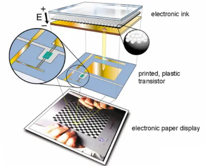
Figure 2.20: Schematic exploded view of the components of a pixel in an electronic paperlike
display (bottom frame) that uses a microcontact printed flexible active matrix backplane circuit (illustration near the bottom frame). The circuit is laminated against an unpatterned thin sheet of electronic ink (top frame) that consists of a monolayer of transparent polymer microcapsules (diameter v100 microns). These capsules contain a heavily dyed black fluid and a suspension of
charged white pigment particles (see right inset). When one of the transistors turns on, electric fields develop between an unpatterned transparent frontplane electrode (indium tin oxide) and a backplane electrode that connects to the transistor. Electrophoretic flow drives the pigment particles to the front or the back of the display, depending on the polarity of the field. This flow changes the color of the pixel, as viewed from the front of the display, from black to white or vica versa.
effects of deformations in the stamp and distortions in the gate and column electrodes that may arise during patterning and processing of the flexible PET sheet. The density of defects in the printed patterns is comparable to (or smaller than) that in resist patterned by contact mode pho-tolithography, when both procedures are performed outside of a cleanroom facility (i.e. when dust is the dominant source of defects).
Figure 2.20 shows an ‘exploded’ view of a paperlike display that consists of a printed flexi-ble plastic backplane circuit like the one illustrated in Figure 2.18 laminated against a thin layer of ‘electronic ink’.25, 55 The ‘electronic ink’ is composed of a monolayer of transparent polymer
microcapules that contain a suspension of charged white pigment particles suspended in a black liquid. The printed transistors in the backplane circuit act as local switches which control elec-tric fields that drive the pigments to the front or back of the display. When the particles flow to the front of a microcapsule, it appears white; when they flow to the back, it appears black.
26 Overview of Stamping Techniques: Methods and Applications
Figure 2.21: Electronic paperlike display showing two different images. The device consists of
sev-eral hundred pixels controlled by a flexible active matrix backplane circuit formed by microcontact printing. The relatively coarse resolution of the display is not limited by material properties or by the printing techniques. Instead, it is set by practical considerations for achieving high pixel yields in the relatively uncontrolled environment of the chemistry laboratory in which the circuits were fabricated.
Figure 2.21 shows a working sheet of active matrix electronic paper that uses this design. This prototype display has several hundred pixels and an optical contrast that is both indepen-dent of viewing angle and significantly better than newsprint. The device is v1 mm thick, it
is mechanically flexible and weighs v80% less than a conventional liquid crystal display of
similar size. Although these displays have only a relatively coarse resolution, all of the pro-cessing techniques, theµCP method, the materials and the ’electronic inks’ are suitable for the
large numbers of pixels that are required for high information content electronic newspapers and other systems. LikeµCP, nTP is well suited to forming high resolution source/drain electrodes
for plastic electronics. nTP of Au/Ti features in the geometry of the drain and source level of organic transistors and with appropriate interconnects on a thin layer of PDMS on PET yields a substrate that can be used in an unusual but powerful way for building circuits: soft, room temperature lamination of such a structure against a plastic substrate that supports the semicon-ductor, gate dielectric and gate levels yields a high performance circuit embedded between two plastic sheets.42, 56 Details of this lamination procedure are presented elsewhere.
2.6 Applications: Unconventional Electronic Systems 27
The left frame of Figure 2.22 shows the current-voltage characteristics of a laminated n-channel transistor that uses the organic semiconductor copper hexadecafluorophthalocyanine (n-type) and source/drain electrodes patterned with nTP. The inset shows an optical micrograph of the printed interdigitated source/drain electrodes of this device. The right frame of Figure 2.22 shows the transfer characteristics of a laminated complementary organic inverter circuit whose electrodes and connecting lines are defined by nTP. The p-channel transistor in this circuit used pentacene for the semiconductor.42
Figure 2.22: The frame on the left shows current-voltage characteristics of an n-channel transistor
formed with electrodes patterned by nanotransfer printing that are laminated against a substrate that supports an organic semiconductor, a gate dielectric and a gate. The inset shows an optical micrograph of the interdigitated electrodes. The frame on the right shows the transfer characteristics of a simple CMOS inverter circuit that uses this device and a similar one for the p-channel transistor.
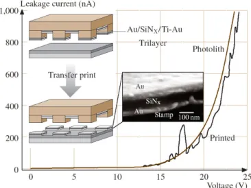
In addition to high resolution source/drain electrodes, it is possible to use nTP to form com-plex multilayer devices with electrical functionality on plastic substrates.43 Figure 2.23 shows
a metal/insulator/metal (MIM) structure of Au (50 nm), SiNx (100nm; by plasma enhanced
vapor deposition, PECVD), Ti (5 nm) and Au (50 nm) formed by transfer printing with a sil-icon stamp that is sequentially coated with these layers. In this case, a short reactive ion etch (with CF4) after the second Au deposition removes the SiNx from the sidewalls of the stamp.
nTP transfers these layers in a patterned geometry to a substrate of Au(15 nm)/Ti(1 nm)-coated PDMS(50µm)/PET(250 µm). Interfacial cold welding between the Au on the surfaces of the
stamp and substrate bonds the multilayers to the substrate. Figure 2.11 illustrates the proce-dures, the structures (lateral dimensions of 250 µm × 250 µm, for ease of electrical probing)
and their electrical characteristics. These MIM capacitors have performance similar to devices fabricated on silicon wafers by photolithography and lift-off. This example illustrates the abil-ity of nTP to print patterns of materials whose growth conditions (high temperature SiNx by
PECVD in this case) prevent their direct deposition or processing on the substrate of interest (PET in this case). The cold welding transfer approach has also been exploited in other ways for patterning components for plastic electronics.50, 57
28 Overview of Stamping Techniques: Methods and Applications
Figure 2.23: Multilayer thin film capacitor structure printed in a single step onto a plastic substrate
using the nanotransfer printing technique. A multilayer of Au/SiNx/Ti/Au was first deposited onto
a silicon stamp formed by photolithography and etching. Contacting this stamp to a substrate of Au/PDMS/PET forms a cold weld that bonds the exposed Au on the stamp to the Au-coating on the substrate. Removing the stamp produces arrays of square (250 µm × 250 µm) metal/insulator/metal capacitors on the plastic support. The dashed line shows the measured current-voltage characteristics of one of these printed capacitors. The solid line corresponds to a similar structure formed on a rigid glass substrate using conventional photolithographic procedures. The characteristics are the same for these two cases. The slightly higher level of noise in the printed devices results, at least partly, from the difficulty in making good electrical contacts to structures on the flexible plastic substrate.
Another class of unusual electronic/optoelectronic device relies on circuits or circuit ele-ments on curved surfaces. This emerging area of research was stimulated primarily by the ability of µCP to print high resolution features on fibers and cylinders. Figure 2.24 shows a
conducting microcoil printed, withµCP using the approach illustrated in Figure 2.4, on a
mi-crocapillary tube. The coil serves as the excitation and detection element for high resolution proton nuclear magnetic resonance of nanoliter volumes of fluid that are housed in the bore of the microcapillary.58 The high fill factor and other considerations lead to extremely high sensiv-itity with such printed coils. The bottom frame of Figure 2.24 shows the spectrum of anv8 nL
volume of ethylbenzene. The narrow lines demonstrate the high resolution that is possible with this approach. Similar coils can be used as magnets,59springs36and electrical transformers.60
2.7 Conclusions 29
Figure 2.24: The top frame shows an optical micrograph of a continuous conducting microcoil
formed by microcontact printing onto a microcapillary tube. This type of printed microcoil is well suited for excitation and detection of nuclear magnetic resonance spectra from nanoliter volumes of fluid housed in the bore of the microcapillary. The bottom frame shows a spectra trace collected from anv8 nL volume of ethyl benzene using a structure similar to the one shown in the top frame.
Figure 2.25 shows an optical micrograph and electrical measurements from a concentric cylindrical microtransformer that uses a microcoil printed on a microcapillary tube with a fer-romagnetic wire threaded through its core. Inserting this structure into the core of a larger microcapillary that also supports a printed microcoil completes the transformer.60 This type of
device shows good coupling coefficients up to relatively high frequencies. Examples of other optoelectronic components appear in fiber optics where microfabriated on-fiber structures serve as integrated photomasks20and distributed thermal actuators.22
Figure 2.25: The inset shows a concentric microtransformer formed using microcoils printed onto
two different microcapillary tubes. The smaller of the tubes (outer diameter 135 microns) has a ferromagnetic wire threaded through its core. The larger one (outer diameter 350 microns) has the smaller tube threaded through its core. The resulting structure is a microtransformer that shows good coupling coefficients at frequencies up tov1 MHz. The graph shows its performance.
2.7
Conclusions
This chapter provides an overview of various soft lithography printing techniques that are capa-ble of micron and sub-micron resolution. It also illustrated some applications where these meth-ods may provide attractive alternatives to more established lithographic method. The growing
30 Overview of Stamping Techniques: Methods and Applications
interest nanoscience and nanotechnology makes crucial the development of new methods for nanofabricating the relevant test structures and devices. The simplicity of these techniques to-gether with the interesting and subtle materials science, chemistry, and physics associated with them, make this a promising area for basic and applied study.
Chapter 3
Improved Surface Chemistries, Thin Film
Deposition Techniques and Stamp Designs
for Nanotransfer Printing
As we have seen in the previous chapter, nanotransfer printing (nTP) represents an additive approach for patterning thin layers of solid materials with nanometer resolution. The surface chemistries, thin film deposition techniques and stamp designs are all important for the proper operation of this method. In this chapter we will present some details concerning processing procedures and other considerations needed for patterning two and three dimensional nanos-tructures with low density of defects and minimal distortions.
3.1
Introduction
Lithographic techniques that use rubber stamps provide simple means to generate patterns with lateral dimensions that can be much smaller than one micron. These soft lithographic printing methods are useful for fabricating devices such as diodes,61 photoluminescent porous silicon
pixels,62 organic light-emitting diodes63 and thin-film transistors.64 and a wide range of other devices in electronics and photonics, as well as biotechnology. The printed inks typically con-sist of soft organic materials such as proteins,65 dendrimers, colloids or molecules that form
self-assembled monolayers.17, 66 Recent work demonstrates that similar stamps can print thin solid inks (i.e. polymer, metal or inorganic films) of functional materials.42, 44, 50, 67 Such meth-ods are purely additive in their operation. They do not suffer from loss of resolution due to etching steps or to surface spreading or vapor phase transport of the inks. One approach, re-ferred to as nanotransfer printing, uses soft or hard stamps to print single or multiple layers of solid films.42, 43, 48, 49 It can form complex two or three dimensional48 structures with
32
Improved Surface Chemistries, Thin Film Deposition Techniques and Stamp Designs for Nanotransfer Printing been used to build plastic42 and molecular electronic devices68, 69 and subwavelength photonic
elements.43 This chapter presents some improved surface chemistries, thin film deposition tech-niques and advanced stamp designs for high fidelity nanotransfer printing of metal films with elastomeric stamps made of poly(dimethylsiloxane) (PDMS). Some of these procedures are also important for a non-invasive electrical probing technique that uses thin metal films on PDMS elements.56, 70, 71 The stamp designs are useful for a range of other soft lithographic methods. Nanotransfer printing (nTP) relies on the transfer of a solid material ink from the structured surface of a stamp to a substrate. Figure 3.1 shows representative procedures for printing thin Au patterns. The process begins with deposition of the Au coating. In the case of figure 3.1, a collimated flux of Au oriented perpendicular to the surface of a stamp forms a discontinuous coating on the raised and recessed regions. Contacting this stamp to a substrate that supports a self-assembled monolayer (SAM) designed to bond to the Au (e.g. a thiol terminated SAM) leads to strong adhesion between the Au and the substrate. Removing the stamp, to which the Au only weakly adheres, transfers the Au on the raised regions of the stamp to the substrate. This purely additive printing approach offers exceptionally high resolution for two dimensional patterning. With specially designed stamps it is possible to transfer complex three dimensional nanostructures. The printing steps can be repeated to build up patterned multilayer stacks.48
Figure 3.1: Schematic illustration of steps for nanotransfer printing. A collimated flux of material
oriented perpendicular to the surface of a high resolution stamp forms a discontinuous coating. (Au is illustrated here. Other materials are possible.) Contacting this coated stamp to a substrate leads to chemical reactions at the interface between the metal and the substrate. (A self assembled monolayer (SAM) provides the necessary chemistry.) These reactions bond the metal to the substrate; removing the stamp (to which the metal only weakly adheres) transfers the metal on the raised regions of the stamp to the substrate. Continuous coatings are also possible. In this case, the transfer process yields certain classes of three dimensional structures.
3.2 Surface Chemistry and Thin Film Deposition Effects on Nanotransfer Printing. 33
3.2
Surface Chemistry and Thin Film Deposition Effects on
Nanotransfer Printing.
The ability to perform nTP depends critically on processing conditions that enable robust coat-ings to be deposited on the stamps and to be transferred from them to substrates without damage. These challenges are significant when relatively brittle materials are printed with the types of elastomeric stamps that have been used in traditional soft lithography. Although nTP is com-patible with rigid stamps, elastomeric ones are attractive because they are easy to fabricate and because they readily form intimate ‘wetting’ contacts with a wide range of substrates without applied pressure. It is therefore important to develop processing conditions for using these types of stamps to fabricate defect free patterns by nTP. The following focuses on printing of Au films onto either silicon wafers (with their native oxide) coated with a bilayer of Ti/Au (2nm/20nm) or onto GaAs wafers coated with a monolayer of octanedithiol. In the former case, cold welding between the freshly evaporated Au layers on the stamp and substrate guides the transfer of the metal patterns.43, 50 In the latter case, Au-S bonds facilitate transfer.44 In both systems, contact
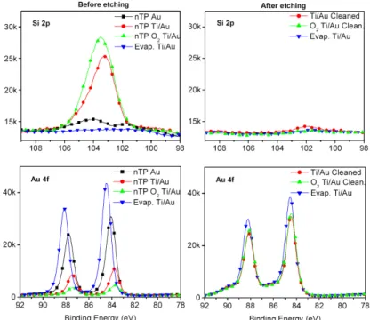
between the stamp and substrate for a few seconds is sufficient to induce bonding. The coating and deposition conditions are chosen to ensure that the strength of adhesion between the metals and the stamps is small compared to the adhesive bonds that form to the substrate during contact. The stamps use bilayer PDMS designs described elsewhere.72 These stamps are placed on glass slides immediately before depositing the Au; they remain on these slides throughout the course of the printing process. Rigid backings help to eliminate damage to the coatings that can otherwise be introduced during manipulation of the stamps. Electron beam evaporation of thin Au (20 nm) onto the stamps at relatively high rates (1 nm/s) yields smooth, electrically continuous coatings that are free of the rippling observed in other work.47 Figures 3.2a-c show
field emission scanning electron micrographs (SEMs) and atomic force micrographs (AFMs) of typical patterns that result from nTP by cold welding onto a silicon substrate (similar results are obtained with the GaAs system). Although printing in this manner successfully forms high resolution patterns over large areas, figure 3.2a-c show that nanoscale cracking in the Au can occur. Imaging of coated stamps before printing (Figure 3.2d) indicates that the nanocracking is already present at that stage of the process.
Contacting and removing the stamp from the substrate, when carried out carefully with stamps mounted on glass slides for support, does not seem to alter significantly the density or length scale of these cracks. This type of defect is often present when only Au is used; it is somewhat less frequently observed when Ti (1-2 nm) is used as an interfacial wetting layer between the Au and PDMS. The morphology and density of these nanocracks seem to be only weakly related to the physical properties (modulus, thermal expansion coefficient, etc.) of the PDMS stamps. (We noticed that evaporated Au films on in situ heated PDMS stamps present identical film structure with a similar density of nano-cracks.) In fact, similar nanocracking is present in 20 nm Au coatings deposited in the same manner onto bare silicon wafers with their