HAL Id: hal-01388035
https://hal.archives-ouvertes.fr/hal-01388035
Submitted on 6 May 2019HAL is a multi-disciplinary open access
archive for the deposit and dissemination of sci-entific research documents, whether they are pub-lished or not. The documents may come from teaching and research institutions in France or abroad, or from public or private research centers.
L’archive ouverte pluridisciplinaire HAL, est destinée au dépôt et à la diffusion de documents scientifiques de niveau recherche, publiés ou non, émanant des établissements d’enseignement et de recherche français ou étrangers, des laboratoires publics ou privés.
Determination of 4H-SiC Ionization Rates Using OBIC
Based on Two-Photon Absorption
Hassan Hamad, Christophe Raynaud, Pascal Bevilacqua, Sigo Scharnholz,
Bertrand Vergne, Dominique Planson
To cite this version:
Hassan Hamad, Christophe Raynaud, Pascal Bevilacqua, Sigo Scharnholz, Bertrand Vergne, et al.. Determination of 4H-SiC Ionization Rates Using OBIC Based on Two-Photon Ab-sorption. Materials Science Forum, Trans Tech Publications Inc., 2016, 858, pp.245 - 248. �10.4028/www.scientific.net/MSF.858.245�. �hal-01388035�
Determination of 4H-SiC ionization rates using OBIC based on two-photon
absorption
Hassan Hamad
1,a*, Christophe Raynaud
1,b, Pascal Bevilacqua
1,c, Sigo Scharnholz
2,d,
Bertrand Vergne
2,e, Dominique Planson
1,f1 INSA de Lyon, Laboratoire Ampère, 21 Avenue Jean Capelle, 69621 Villeurbanne Cedex, France. 2 French-German Research Institute of Saint Louis (ISL), 5 Rue du Général Cassagnou, 68301 Saint-Louis
Cedex, France.
a[email protected], b[email protected], c[email protected], d[email protected], e[email protected], f[email protected]
Keywords: OBIC, two-photon absorption, Ionization rates, 4H-SiC, avalanche diodes, high electric field.
Abstract: Optical Beam Induced Current (OBIC) measurements are performed on 4H-SiC avalanche diodes with a very thin and a highly doped active region. A pulsed green laser, with a wavelength of 532 nm, illuminates a reverse biased diode leading to generate electron-hole pairs in the space charge region. Comparison between the 4H-SiC bandgap and the incident photon energy shows that single photon absorption process can be neglected and two-photon absorption process dominates in this case. Ionization rates are then extracted from multiplication curve in a high electric field range (3 to 5 MV.cm–1). Results are in good agreement with previous ones obtained on the same diodes using single photon absorption process.
Introduction
4H-SiC becomes widely used for power device application due to its high critical electric field, high thermal conductivity and technology maturity. However, further reaching studies of breakdown limiting factors are needed to improve the understanding of device breakdown. In this stage, ionization rates are required to predict the breakdown voltage of electronic devices. They are defined as the number of generated charge carriers by collisions per length unit from one charge carrier. Ionization rates are used in numerical simulators like SENTAURUS TCAD [1] in order to predict the leakage current and the breakdown of the devices. They are rarely studied and results already published are, more or less, scattered [2-6]. Many methods like OBIC or EBIC (Optical/Electron Beam Induced Current) are used to determine the ionization rates. In this paper, OBIC method based on two-photon absorption process is used in 4H-SiC in order to extract ionization rates from the multiplication curve.
OBIC principle
When an optical beam illuminates perpendicularly a reverse biased PN junction, photon absorption leads to generate electron-hole pairs (EHPs). According to the wave length (respectively the photon energy EΦ), the absorption of one photon can lead to generate an EHP if EΦ is high enough compared to the semi-conductor bandgap EG (EΦ > EG). If EΦ is smaller than EG (EΦ < EG), one-photon absorption process becomes impossible and then two or more photons must interact at the same time with an atom to be absorbed and to generate an EHP. This is the multi-photon absorption process that has been theoretically predicted in 1931 [7]. Since the two-photon absorption probability is weak compared to single photon absorption process, high beam power densities are necessary to generate EHPs. Moreover, two-photon absorption process takes place in a more confined region, allowing a better spatial resolution (compared to single photon absorption). Two-photon absorption process was recently demonstrated on 4H-SiC by using a green laser beam (532 nm) [8]. In this work, two-photon absorption is investigated using the same green laser on 4H-SiC devices.
EHPs generated outside the space charge region (SCR) are not submitted under electric field, they will recombine and no effect is measured. EHPs created in the SCR will be accelerated by the electric field and thus an induced current is measured, hence the naming of the method: Optical Beam Induced Current OBIC (Fig. 1). For voltages close to the breakdown voltage VBR, the electric field becomes high; the EHPs gain a kinetic energy and collide with the atoms in the crystalline
structure leading to the generation of a new EHPs, which in turns may lead to the creation of new EHPs; this is manifested by an increase of the OBIC signal. The multiplication coefficient M is defined as the ratio between the induced current Jph at a given voltage V and at V0 (for which there is no multiplication) as shown in eq. 1.
𝑀(𝑉) = 𝐽'((𝑉) 𝐽'((𝑉))=
𝑀*𝐽*+𝑧'- + 𝑀'𝐽'(𝑧*) + 𝑀/01𝐽/01
𝐽'((𝑉)) . (1)
where Mn (Mp, MSCR) is electron (resp. hole, SCR) multiplication coefficient, Jn and Jp are the minority carrier currents at the edges of SCR, JSCR is the photo-generated current inside the SCR. Minority currents can be found by solving the continuity equations of charge carriers and taking into account the limit conditions [6].
To determine ionization rates, different authors have proposed models for ionization rates [9-11] by taking into account some physical approximations or by giving empirical equations. During a free mean path, the energy acquired by a charge carrier depends on the electric field. This means that ionization rates of a material depend only on material characteristics and the electric field. In this work, Chynoweth model is used to calculate ionization rates of electrons an and holes ap (eq. 2). This is an empirical model that assumes that only charge carriers that reach ionization energy during a free path contribute to impact ionization [11].
𝛼*,'(𝐸) = 𝐴*,'exp 9−𝐵*,'< = . 𝐸 (2)
where E is the electric field, An,p and Bn,p are two constants depending on the semiconductor. Experimental setup
In this paper, OBIC measurements are realized using a pulsed green laser at 532 nm (Erreur ! Source du renvoi introuvable.). The repetition frequency is 20 kHz and the pulse duration is ~1 ns. Mean optical power can be modified up to 100 mW. The pulse energy can reach up to 5µJ (or an instantaneous power of 5 kW). Optical beam is guided through two semi-reflecting mirrors and it is focused through a focusing lens. The mirrors and the lens are piloted to control the focus spot position which is of 10 µm diameter.
Instantaneous optical power density can reach up to 6.4 GW.cm–2.
For this wavelength (532 nm), a focused beam leads systematically to scratch the device surface and then its destruction. The solution is to defocus the beam so that the focus will be above the device under test (DUT) and the beam reaches the DUT with a diameter of 15 µm. This solution works well, optical power remains high at this point and no scratches are observed on the DUT
Fig. 1: Cross-sectional view of a reverse biased PN junction to illustrate the OBIC principle.
The DUT is the same circular avalanche diode, with a breakdown voltage of 59 V, as already used in previous studies [5, 6, 8, 12]. It presents a thin and highly doped active layer, which means high electric field devices (> 3 MV.cm–1). A 100×100 µm2 optical window was performed using SIMS technique on some diodes (fig. 3) allowing the optical beam to penetrate towards the drift region of the diode [12]. Results and discussion
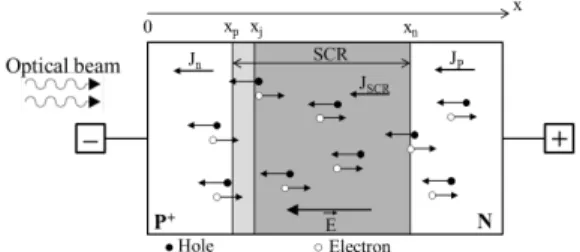
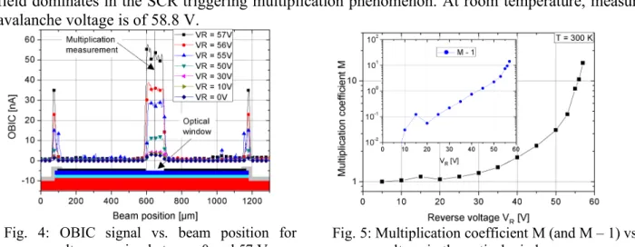
Figure 4 shows the OBIC signal vs. beam position for different reverse voltages. An important OBIC signal is measured when the beam illuminates the optical window. OBIC signal is null when illuminating the metallization. To deduce the multiplication curve, OBIC signal obtained in the optical window is only studied; figure 5 shows then multiplication curve vs. reverse voltage (the reference voltage V0 taken in this stage is 5 V). For low voltages (< 40 V), electric field is low even in the SCR so that multiplication can be neglected. When VR increases near VBR, a strong electric field dominates in the SCR triggering multiplication phenomenon. At room temperature, measured avalanche voltage is of 58.8 V.
Fig. 4: OBIC signal vs. beam position for reverse voltage varying between 0 and 57 V.
Fig. 5: Multiplication coefficient M (and M – 1) vs. reverse voltage in the optical window.
A 1D numerical model of the diode is simulated in order to determine ionization rates. Its input parameters are given by the semiconductor material, the regions depth and doping levels of the diode, as well as the optical beam characteristics. It computes for each voltage: the electric field at each depth in the diode, the absorption rate, the photo-generated current and then the multiplication coefficient. Measured multiplication curve is fitted with simulated one by changing the ionization rates. An error function ΔM is then defined as shown in eq. 3, and the aim is to minimize ΔM when changing ionization rates. The parameters An, Bn, Ap, and Bp leading to the minimum of ΔM are supposed to be the true ones. Table 1 shows the parameters of αp and αn and figure 6 shows the experimental M curve and simulated one.
∆𝑀 = ? +𝑀@− 𝑀B-A C
DEF
DGHDI
. (3)
where Mi and 𝑀B are respectively measured and computed multiplication coefficient at the reverse A voltage Vi.
Table 1: Parameters of ionization rates for 4H-SiC for high electric field range (3 to 5 MV.cm–1).
Ap [106 cm–1] Bp[107 V.cm–1] An [106 cm–1] Bn [107 V.cm–1] ΔM VBR [V]
1.71 1.18 1.11 1.22 0.724 59.2
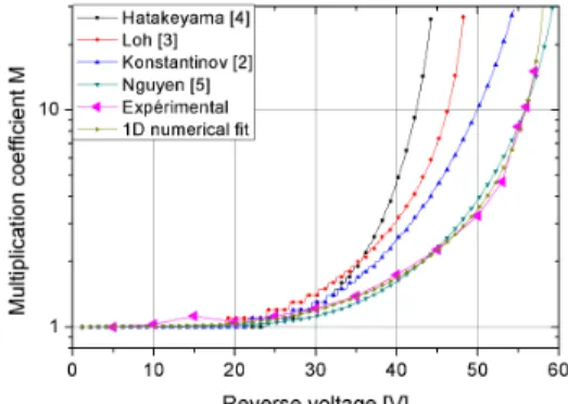
The scattered ionization rates found in literature are in the origin of the gap found for the multiplication curve and then the breakdown voltage. This difference is due to the doping level of the DUTs and the method used to extract ionization rates. To validate our results, a comparison of ionization rates is realized between this case and the case of single photon absorption (OBIC measurements with an incident beam of 349 nm of wavelength) realized with the same DUT. Results show that the found ionization rates are almost the same using OBIC method but with different wavelength and absorption process (fig. 7). In addition, these results are compared to other published ones (fig. 8); comparison shows that the hole’s ionization rates αp are greater than electron’s ionization rates αn (as the other authors) but the ratio αp/αn is about twice (much smaller than the published results). Note that the found results are applicable only for high electric field range (3-5 MV.cm–1). Conclusion
In this paper, ionization rates in 4H-SiC are extracted for high electric field range (3 to 5 MV.cm–1) using OBIC method. Optical beam is performed using a green laser (532 nm). Photon energy is much smaller than semiconductor bandgap, thus, two-photon absorption process takes place allowing a better spatial resolution (compared to single photon absorption). Results of ionization rates are in good agreement with other ones obtained on the same DUTs using single photon absorption OBIC. Results show also that hole’s ionization rate is greater than electron’s ionization rate (as other authors), however the ratio αp/αn is about twice (much smaller than the published results). References
[1] “Sentaurus Device User Guide Version F-2011, http://www.synopsys.com/home.aspx.
[2] A-O. Konstantinov, Q. Wahab, et al., Materials Science Forum, vols. 264-268, 513 (1998).
[3] W. S. Loh, B. K. Ng, et al., Electron Devices, IEEE Transactions on, vol. 55, n°. 8, p. 1984 (2008). [4] T. Hatakeyama, T. Watanabe, et al., Applied Physics Letters, vol. 85, n°. 8, p. 1380 (2004).
[5] D-M. Nguyen, C. Raynaud, et al., Materials Science Forum, vols. 717-720, 545 (2012). [6] H. Hamad, C. Raynaud, et al., Materials Science Forum, vols. 821-823, 223 (2015). [7] M. Goeppert-Mayer, Ann. Phys, vol. 9 p.273 (1931).
[8] H. Hamad, C. Raynaud, et al., Applied Physics Letter, vol. 104, p. 082102, 2014. [9] P. A. Wolff, Physical Review, vol. 95, n°. 6, p. 1415 (1954).
[10] G. A. Baraff, Physical Review, vol. 128, n°. 6, p. 2507 (1962).
[11] A-G. Chynoweth, Journal of Applied Physics, vol. 31, n°. 7, p. 1161 (1960). [12] M. Lazar, F. Jomard, et al., Materials Science Forum, vols. 717-720, 885 (2012).
Fig. 6: Comparison of measured and simulated multiplication curve.
Fig. 7: Ionization rates vs. electric field with green and UV lasers.
Fig. 8: Ionization rates vs. electric field compared with other authors.