HAL Id: hal-01387924
https://hal.archives-ouvertes.fr/hal-01387924
Submitted on 2 May 2019
HAL is a multi-disciplinary open access
archive for the deposit and dissemination of sci-entific research documents, whether they are pub-lished or not. The documents may come from teaching and research institutions in France or abroad, or from public or private research centers.
L’archive ouverte pluridisciplinaire HAL, est destinée au dépôt et à la diffusion de documents scientifiques de niveau recherche, publiés ou non, émanant des établissements d’enseignement et de recherche français ou étrangers, des laboratoires publics ou privés.
Optical beam induced current measurements based on
two-photon absorption process in 4H-SiC bipolar diodes
Hassan Hamad, Christophe Raynaud, Pascal Bevilacqua, Dominique Tournier,
Bertrand Vergne, Dominique Planson
To cite this version:
Hassan Hamad, Christophe Raynaud, Pascal Bevilacqua, Dominique Tournier, Bertrand Vergne, et al.. Optical beam induced current measurements based on two-photon absorption process in 4H-SiC bipo-lar diodes. Applied Physics Letters, American Institute of Physics, 2014, 104 (8), �10.1063/1.4866581�. �hal-01387924�
1
Optical Beam Induced Current Measurements Based on
Two-Photon Absorption Process in 4H-SiC Bipolar Diodes
H. HAMADa, C. RAYNAUDa, P. BEVILACQUAa, D. TOURNIERa, B. VERGNEb and D. PLANSONa a Ampère Laboratory - UMR 5005, 21, Avenue Jean Capelle, 69621 VILLEURBANNE CEDEX, FRANCE b Franco-Allemand Institute of Saint-Louis ISL
5, Rue du Général Cassagnou, 68300 SAINT-LOUIS, FRANCE
Abstract: Using a pulsed green laser with a wavelength of 532 nm, a duration pulse of ~1ns, and a mean power varying between 1 and 100 mW, induced photocurrents have been measured in 4H-SiC bipolar diodes. Considering the photon energy (2.33 eV) and the bandgap of 4H-SiC (3.2eV), the generation of electron-hole pair by the conventional single photon absorption process should be negligible. The intensity of the measured photocurrents depends quadratically on the power beam intensity. This clearly shows that they are generated using two-photon absorption process. With the two-photon absorption process, laser beam can reach deeper parts in the semiconductor before it is absorbed. As in conventional OBIC, the measurements give an image of the electric field distribution in the structure under test, and the minority carrier lifetime can be extracted from the decrease of the photocurrent at the edge of the structure. The extracted minority carrier lifetime of 210 ns is consistent with results obtained in case of single photon absorption.
Key-words: 4H-SiC, two-photon absorption, OBIC, bipolar diodes
I. INTRODUCTION
Electron and Optical Beam Induced Current (EBIC and OBIC) techniques have been widely used to determine carrier lifetimes [1], but also impact ionization coefficients in silicon and silicon carbide devices [2]. The principle of these techniques consists in creating a free carrier pair by ionization of a lattice atom due to the absorption of a photon in case of OBIC [3], or due to the kinetic energy transfer of an electron in case of EBIC [4].
With the emergence of wide band gap semiconductor (WBG), power semiconductor devices are expected to know an important breakthrough. Silicon carbide is the most promising WBG in replacing silicon power devices, but other WBG such as diamond could also be excellent candidates provided that their technology is more mature. The main interesting properties of the WBG for power electronics are their high critical electric field, very low leakage currents in blocking states and a 3 times higher thermal conductivity than silicon. These properties permit to realize high voltage system exhibiting same performances but downsized or very high voltage devices that are not possible with silicon. Designing such power devices needs to optimize the periphery of the active region, to limit the strengthening of field lines. As a consequence, OBIC has been used to experimentally verify the distribution of the electric field in the periphery of the devices [5]. Up to now, majority of OBIC published results are based on the absorption of a single photon, whose energy EΦ must be necessarily larger than the semiconductor bandgap EG.
Therefore in silicon carbide and diamond, it is necessary to use UV-beam (wavelength of 380 nm in SiC and 225nm in C). In failure analysis of silicon integrated circuits, a two-photon OBIC (TOBIC) technique have been successfully demonstrated [6] and advantageously compared to the single photon OBIC [7]. Two-photon absorption has been predicted in 1931 by M.
Goeppert-2
Mayer [8]. This effect is a third order optical effect, and therefore is detectable only under high intensities of light. Thirty years later, the invention of laser allowed to experimentally verify this phenomenon in a large number of crystals and liquids and for the first time in a semiconductor in 1964 [9]. In 1999, TOBIC have been used to study InGaN blue light emitting diodes Erreur ! Source du renvoi introuvable. The main advantage is that TOBIC requires two seemingly contradictory conditions: the incident beam must efficiently generate carriers in the active layer but must not be absorbed or scattered by the overlayers or by the substrate. Hence free carrier generation is confined in the vicinity of the focal point. We demonstrate here the first TOBIC measurements in silicon carbide diodes.
II. SINGLE AND TWO PHOTON OBIC PRINCIPLE
Illuminating a pure semiconductor with a focused light beam will generate electron-hole pairs (EHPs) by absorption of photons. Selecting an appropriate wavelength induces the predominance of single photon or two photon absorption. If the wavelength is chosen so that the photon energy EΦ is less than the bandgap EG, single photon absorption cannot produce an EHP and the generation
of free carriers is mainly due to two-photon absorption. If EG < EΦ < 2EG, both mechanisms coexist
[10]. In reality for EΦ ≲ EG, creation of excitons can be possible, but if (2EΦ-EG) ≥ exciton binding
energy (20meV in 4H-SiC), it has been shown that two-photon transition based on excitonic states can be ignored [9]. It is also interesting to note that SiC is an indirect bandgap semiconductor so that phonons are involved in the absorption process and in the subsequent generation of electron-hole pairs.
It is well known that single photon absorption coefficient a is related to the incident light intensity transmitted through a layer of material by the empirical Beer Lambert law:
𝑑𝐼
𝑧 = −𝛼𝐼 (1)
where I is the incident light intensity, and z the thickness of the layer.
Considering nonlinear effects, the theory demonstrates that the two photon absorption b is defined as:
𝑑𝐼
𝑧 = −𝛽𝐼² (2)
In order to illustrate the OBIC technique, we can consider the P+/N junction shown in Figure
1. Once, it is reverse biased, the space charge region (SCR) will extend mainly in the low-doped zone which is n-type. Increasing the reverse voltage will induce a high electric field in the SCR. When the laser beam is applied perpendicularly to the PN junction, the EHPs created inside the SCR are separated due to the electric field and accelerated up to its limits. The resulting current is then measured. Outside the SCR, the generated EHPs will diffuse and recombine and no current will be measured. If the distance between generated EHPs and the SCR is smaller than their diffusion length, they may reach its edge and an OBIC is also measured. This OBIC current is proportional to the incident power Pbeam in case of single photon absorption, and varies as the
square of Pbeam for two-photon absorption.
III. EXPERIMENTAL SETUP
In this work, a green laser is applied on 4H-SiC diodes. Since Eφ is 2.33eV, and Eg is 3.26eV,
3
(532 nm) with pulse duration of about 1ns and repetition frequency of 20 kHz. The beam is then directed by mirrors and focused on the samples by a lens with a focal length of 10 cm. Mirrors and the lens are moved by piezoelectric motors with a minimum step of 1µm, so that it is possible to displace the beam on the whole surface of the sample, and to vary the depth of the focal point with respect to the sample surface (Figure 2). When focusing, the spot diameter is about 10µm and beam power density can reach 6.6 GW.cm-2, so that two-photon absorption can possibly occur.
This power density can be reduced by rotating a polarizer, and the transmitted power has been calibrated as a function of the angle.
Electrical contact on the front side (anode) is made with a thin tip. On the backside, the sample is glue on a conductive support. The mean current is measured using a Keithley Source Measurement Unit K237, with sensitivity less than 1pA.
First sample studied is a MESA protected circular Zener diode produced by the research Institute of Saint-Louis (ISL). It is composed by a 2.2µm thick P+ layer and a thin epitaxial
transition layer P deposited on an N+ substrate. An optical window is performed through the
metallization (Figure 3a) [11]. These Zener diodes show breakdown voltage of ~60V and have been ever studied by single photon OBIC [12]. Second sample is a square P+N–N+ diode protected
by a junction termination extension (JTE) layer to avoid local breakdown at peripheries. Surface passivation and field plate are added to provide a higher breakdown voltage of ~800V (Figure 3b). A preliminary work is to select the appropriate diodes to be studied. The photocurrents measured by OBIC setup are strongly dependent of reverse voltage, beam position and beam power, but they must remain weak to avoid the breakdown of the sample. Moreover, as the K237 unit measured a mean current over a duration of several ms, the studied diodes must have low leakage current IL to not mask the photocurrent. A dark leakage current of 10 nA has been chosen
as maximum acceptable value: only 10% of diodes are suitable for OBIC tests. IV. RESULTS AND DISCUSSION
It is important to note that focusing the beam lead to systematically destroy the diodes if the beam illuminates the metal. This destruction means that the diode does not block any current in reverse state. Physically, micromachining initiates on metal parts and then it keeps carving on SiC. So measurements have been performed with a defocused beam to avoid destruction of the test diodes. We used a divergent beam with a diameter of about 20 µm on the substrate.
Figure 4 shows the variation of the photocurrent intensity measured on both samples for low reverse voltage as a function of the beam power density. The laser beam illuminates in the optical window for ZENER sample and in the JTE for PN one. It is clear that OBIC is a parabolic function of beam power. For comparison, similar curves reported in [7] are plotted on only one decade of power (from 0.5 to 10 mW). As a consequence, it proves that two-photon absorption occurs in 4H-SiC and generates electron-hole pairs.
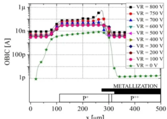
OBIC is measured as function of beam position for several reverse voltage values along a part of a diameter (Figure 5). An OBIC is measured when laser beam is on the optical window and on the MESA etching and it is null elsewhere.Figure 6shows OBIC vs. beam position along the half-length of a PN diode (sample 2) for different voltage values. As expected, an OBIC signal is measured when the beam is sweeping the high electric field zone. It is null elsewhere and when
4
the beam is above metallization, it is assumed to be a reflecting surface. As we noticed before, OBIC gives an image of the electric field distribution: curves shown in Figure 6 do nothave peaks for VR ≤ 700V; this means that electric field is almost constant along the JTE. Carrier lifetime τ
can also be deduced from the edge of OBIC signal [7] at this zone, OBIC decreases exponentially as a function of distance z with SCR as given by:
𝐽(𝑧) = 𝑢 exp 1−𝑧
𝐿34 (3)
where Ld is the diffusion length, u the optical generation rate. Experimental values of Ld is
determined to be 14.75µm and then, the minority carrier lifetime is 210 ns using 𝜏 = 𝐿3
7𝑞
𝑘𝑇𝜇
(4) where q, k, T and µ = 400 cm²V-1s-1 are electron charge, Boltzmann constant, temperature and
carrier mobility respectively. These results are in a good agreement with values obtained with single-photon OBIC measurements in SiC [5].
V. CONCLUSION
We have performed OBIC measurements on 4H-SiC bipolar diodes using a green laser with an energy widely less than the bandgap of the semiconductor. The measured induced photocurrent depends quadratically with the incident beam power. This clearly demonstrates that the photocurrent is generated by a two photon absorption process. To our best knowledge, it is the first time that this process is experimentally used in silicon carbide device characterization. Lifetime values deduced from these measurements are in agreement with values obtained in conventional OBIC (using single photon absorption). Further improvements of the setup allow placing the sample in vacuum in order to perform OBIC measurements up under reverse bias up to several kV.
VI. ACKNOWLEDGEMENTS
The authors thank Dr. SCHARNHOLZ Sigo from ISL to permit us to realize many measurements at ISL and to provide a lot of test diodes to realize this work. Acknowledgements are also due to Dr. BROSSELARD Pierre for helpful discussions and TRACE program for financial support.
VII. REFERENCES
[1] T. Flohr and R. Helbig, Journal of Applied physics, vol. 66, no. 7, p. 3060, 1989. [2] R. Raghunathan and B.J. Baliga. Solid-State Electronics 43, pp.199-211, 1999.
[3] C. Raynaud, S. R. Wang, D. Planson, M. Lazar and J. P. Chante, Diamond & Related Materials, vol. 13, p. 1697, 2004.
[4] O. Lopatiuk-Tirpak and L. Chernyak, Applied Physics Letters, vol. 89, 142114, 2006.
[5] C. Raynaud, D. M. Nguyen, N Dheilly, D. Tournier, P Brosselard, M. Lazar and D. Planson, Physica Status Solidi A, no. 10, p. 2273, 2009.
[6] C. Xu and W. Denk, Applied Physics Letters, vol. 71, number 18, p. 2578, 1997. [7] C. Xu and W. Denk, Journal of Applied Physics, vol. 86, number 4, p. 2226, 1999. [8] M. Goeppert-Mayer, Ann. Phys. Vol.9 p.273, 1931.
[9] R. Braunstein and N. Ockman. Physical Review, vol.134,n°2A, p.499, 1964.
[10] F. Adduci, I. M. Catalano, A. Cingolani and A. Minafra. Physical Review B, vol.15, n°2, p. 926, (1977). [11] M. Lazar, F. Jomard, D.M. Nguyen, C. Raynaud, G. Pâques, S. Scharnholz, D. Tournier and D. Planson.
Materials Science Forum, vol. 717-720, p. 885, 2012.
[12] D.M.Nguyen, C.Raynaud, M.Lazar, G.Pâques, S.Scharnholz, N.Dheilly, D.Tournier and D.Planson. Materials Science Forum, vol. 717-720, p.545, 2012.
5
Figure 1: Reverse biased PN junction illuminated with a laser beam.
Figure 2: Schematic view of experimental OBIC bench.
Figure 3: Cross section view of a part of test diodes: (a) ZENER Diode and (b) PN diode.
Figure 4: OBIC vs. Beam power density (-●- for ZENER diode and -■- for PN diode).
Figure 5: OBIC vs. beam position for ZENER diode with optical window for several reverse voltages.
Figure 6: OBIC vs. beam position for different reverse voltage values for PN diode.