HAL Id: hal-02975956
https://hal.archives-ouvertes.fr/hal-02975956
Submitted on 23 Oct 2020HAL is a multi-disciplinary open access
archive for the deposit and dissemination of sci-entific research documents, whether they are pub-lished or not. The documents may come from teaching and research institutions in France or abroad, or from public or private research centers.
L’archive ouverte pluridisciplinaire HAL, est destinée au dépôt et à la diffusion de documents scientifiques de niveau recherche, publiés ou non, émanant des établissements d’enseignement et de recherche français ou étrangers, des laboratoires publics ou privés.
Study of 4H-SiC high voltage bipolar diodes under
reverse biases using electrical and Obic characterization
K Isoird, M Lazar, Marie-Laure Locatelli, Christophe Raynaud, Dominique
Planson, Jean-Pierre Chante
To cite this version:
K Isoird, M Lazar, Marie-Laure Locatelli, Christophe Raynaud, Dominique Planson, et al.. Study of 4H-SiC high voltage bipolar diodes under reverse biases using electrical and Obic characterization. ICSCRM, Oct 2001, Tsukuba, Japan. �hal-02975956�
Study of 4H-SiC High Voltage Bipolar Diodes Under Reverse Biases
Using Electrical and OBIC Characterizations
K. Isoird
1, M. Lazar
1, M.L. Locatelli
2, C. Raynaud
1, D. Planson
1, J.P. Chante
11CEGELY (UMR CRNS 5005), INSA de Lyon, bât. Léonard de Vinci, 20 Av. A. Einstein, F-69621
Villeurbanne cedex, France.
2LGET (UMR CNRS 5003), Université Paul Sabatier, 118 route de Narbonne, F-31062 Toulouse
cedex 4, France
Keywords: OBIC, JTE, Bipolar diode, Breakdown Voltage, Surface charge.
Abstract. 4H-SiC P+NN+ structures have been fabricated following MediciTM software simulation in
order to block voltages as high as 6 kV. In particular, these diodes are realized by surrounding the emitter by a Aluminum-implanted ring called Junction Termination Extension (JTE). Electrical
characterizations under reverse bias at room temperature and in various environments (air, SF6) show
a premature breakdown of the diodes. This breakdown is localized at the emitter periphery. OBIC (Optical Beam Induced Current) measurements show a peak of photocurrent at the emitter junction edge, indicating the presence of a high electric field. These results involve an effectiveness of 60 % of the JTE. This is probably related to a low electrical activation of the implanted aluminum during the post-implantation annealing and to the presence of positive charges at the surface of the devices.
Introduction.
Silicon carbide presents interesting electrical properties for many applications and especially for the high voltage devices. To fully benefit the advantages of SiC and avoid any premature breakdown of the high voltage diodes, it is necessary to realize efficient junction terminations. The purpose of this work is to estimate the Junction Termination Extension (JTE) influence on the electrical behavior of
4H-SiC P+NN+ diodes under reverse biases. In this paper we present current-voltage (I-V)
characteristics measured in two different gaseous ambients (air, SF6). Analyses of these results are
completed by OBIC (Optical Beam Induced Current) measurements. This technique allows to investigate the electric field distribution in the structure and especially at the junction periphery.
Experiments Device structure
P+NN+ diodes are formed by multiple aluminum implantations at room temperature in n-type 4H-SiC
epilayer (thickness = 40 µm, doping level = 1.1´1015 cm-3 confirmed by C(V) measurement over a
few µm depth from the surface). The JTE is created by five successive aluminum implantations at room temperature. Main parameters of the junction termination (depth = 0.5 µm, doping level =
2´1017 cm-3, length = 250 µm) are optimized with MediciTM software simulations (the ionization
coefficients used are those given by Konstantinov et al. [1]) in order to obtain blocking voltages as high as 6 kV. Then the samples are annealed at 1700 °C during 30 minutes [2], and finally metallized for both anode and cathode ohmic contacts. No passivation layer covers the semiconductor surface. Two types of diodes are tested : diodes without JTE (D1), and diodes with JTE region (D2).
OBIC setup and method
The OBIC method has been previously used to investigate the influence of JTE on the electric field distribution in bipolar diodes. For photo-excitation a UV light is used at different wavelengths (ranging from 363.8 nm down to 300 nm) which is focused at the surface of the sample and modulated at 70 Hz by a chopper. The curves are obtained by scanning a diameter of the diode (400 µm diameter)
with the laser beam (3.3 µm diameter). The detailed descriptions of the OBIC method and setup are given in Reference [3].
Results.
Electrical characterizations.
The I-V characteristics and tests of breakdown voltages were realized under DC conditions at room
temperature in two different ambients (air and SF6 gas). The demonstrations of the breakdown were
observed by means of a CCD camera and a video monitor. The forward I-V characteristics present
good rectifying behaviors: the typical forward drop voltage at 300 K is 3 V at 10 A cm-². Under
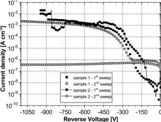
reverse bias in air ambient at 300 K, the curve presents two distinct zones (Fig. 1). In the first part of
the initial characteristic, the current remains weak up to a reverse bias VR of -200 V. Beyond this
voltage, the current rises quickly until VR = -400 V and tends to saturate in the range [10-4- 10-3]
A/cm². When VR < -500 V, electric arcs begin to appear between the anode contact and some close
etched or metallized devices. This I-V curve is not reproducible. During the second measurement in the first part, we observe an increase of the current. For the second part of the characteristic, we note that for a same voltage the measured current is generally weaker. Those results are completed by I-V
measurements performed in SF6 ambient under small overpressure (Fig. 2). In these conditions we
observe the same behavior than in the air ambient. However, luminous white points at the emitter periphery accompany the electric arcs. Towards 2000 V the arcs lead to the diode breakdown. This
illustrates a localized breakdown of the diode induced by a high electric field at the P+N junction
edge. For the diodes without junction termination, the maximum breakdown value reached is in the range [700-1000] V, these results are in good agreement with those obtained by MEDICI simulations.
Fig. 1: Reverse electrical characteristics of diodes with JTE (D2), measured at 300 K in the air. Two bias sweeps are presented for each diode. The order of appearance in the legend corresponds to the chronological order of I-V measurement performed on each diode.
Fig. 2: Reverse electrical characteristics of
diodes with JTE, measured at 300 K in the SF6
ambient using a Tektronix 370A curve tracer. Three bias sweeps are presented for this diode and are numbered in the order of measurement.
OBIC measurements
Fig. 3 shows OBIC measurements performed on a D1 diode along a diameter line using 363.8 nm wavelength corresponding to a penetration length in 4H-SiC higher than 40 µm [4]. We observe an OBIC signal when the spot light illuminates the emitter non-covered by the metal. The photocurrent increases with the reverse voltage due to the space charge region (SCR) spreading inside the epilayer.
At VR = -300 V, a peak of photocurrent emerges at the emitter edge, which indicates carriers
multiplication due to a localized high electric field. -1050 -900 -750 -600 -450 -300 -150 0 10-10 10-9 10-8 10-7 10-6 1x10⁻⁵ 1x10⁻⁴ 10-3 10-2 10-1 sample 1 - 1st sweep sample 1 - 2nd sweep sample 2 - 1st sweep sample 2 - 2nd sweep Reverse Voltage [V] Cu rr en t d en si ty [ A cm -2 ] 0 400 800 1200 1600 2000 0 1x10⁻² 2x10⁻² 3x10⁻² 4x10⁻² 5x10⁻² 6x10⁻² 7x10⁻² 3 2 1 Reverse Voltage [V] Cu rr en t d en si ty [ A cm -2 ]
Fig. 3: OBIC measurements performed on a D1
diode without JTE at l = 363.8 nm with Popt =
2 for different reverse voltages.
Fig. 4: OBIC measurements performed on a D2
diode with JTE at l = 363.8 nm with
Popt = 2 for different reverse voltages.
The OBIC signal measured on a D2 diode with JTE (Fig. 4) presents the same behavior. No
photocurrent is detected over JTE position but we recognize the signal due to the P+N junction which
increases with the reverse voltage. However at VR = -300 V we detected a weak signal on the part of
JTE close to the emitter. In order to observe the effect of JTE on electric field distribution it is necessary to investigate a lower depth of the epilayer by measuring OBIC signal using a shorter wavelength.
Fig. 5: OBIC measurements performed on a D2 diode with JTE at l = 300 nm with Popt = 2
for different reverse voltages.
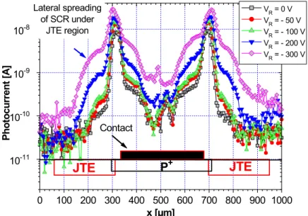
Fig. 5 shows OBIC measurements on a D2 diode illuminated at a wavelength of 300 nm. Contrary to
the curves obtained at l = 363.8 nm, at VR = 0 V we detected an OBIC signal on part of JTE. This
photocurrent increases with the voltage and we also note that when the bias increases, the area where the signal is detected extends laterally. Those results illustrate the lateral spreading of the SCR under JTE region [5] that indicates a total depletion of JTE.
Discussion.
The electrical results have shown a premature breakdown of diodes with junction termination. SIMS analyses at different places on a wafer reveal an aluminum implanted dose of JTE lower than the
0 100 200 300 400 500 600 700 0 1x10⁻⁹ 2x10⁻⁹ 3x10⁻⁹ 4x10⁻⁹ N P+ x [µm] Ph o to cu rr en t [A ] VR = - 300 V VR = - 200 V VR = - 100 V VR = 0 V -2 W cm 0 100 200 300 400 500 600 700 800 900 0,0 5,0x10⁻¹⁰ 1,0x10⁻⁹ 1,5x10⁻⁹ 2,0x10⁻⁹ 2,5x10⁻⁹ JTE P+ JTE x [µm] Phot oc ur re nt [ A ] VR = - 300 V VR = - 200 V VR = - 100 V VR = - 50 V VR = 0 V -2 W cm 0 100 200 300 400 500 600 700 800 900 1000 10-11 1x10⁻¹⁰ 1x10⁻⁹ 1x10⁻⁸ Lateral spreading of SCR under JTE region JTE P+ JTE Contact x [µm] Ph o to cu rr en t [A ] VR = 0 V VR = - 50 V VR = - 100 V VR = - 200 V VR = - 300 V -2 W cm
desired one (1´1013 cm-2). The simulations carried out with these effective JTE doping values give a
theoretical breakdown voltage (3 kV) higher than experimental value. Measurements obtained with OBIC method show an premature depletion of the JTE area and a localized breakdown at the emitter edge. Those results tend to confirm a certain protection inefficiency probably due to an aluminum
electrical activation1 lower than 100 % [3]. However the low aluminum electrical activation does not
seem to be the only explanation of the poor JTE efficiency. Indeed OBIC measurements performed on several diodes have revealed the presence of a high electric field at the emitter edge under weak voltages. Those results and the instability of current during I-V measurements can be due to the presence of a surface charge. The different steps of the process flow are certainly at the origin of this surface charge. Indeed the presence of a positive charge on the SiC surface tends to tighten the equipotential lines at the junction periphery which induces a degradation of the JTE performance [6] and causes the appearance of high electric field at the emitter edge. This last assumption seems to be
confirmed by simulation of D1 and D2 diodes with a positive charge density of 7´1011 cm-2. We note
that the positive charge has no influence on the breakdown value of D1 diodes. On the contrary, by comparing the results of D1 diode simulation with or without surface charge, we observe for a same voltage an increase of the electric field at the emitter periphery. For the D2 diode we clearly observe an effect of surface charge on the JTE performance. By taking account of the positive surface charges, the efficiency of junction termination is reduced by about 12 %. The premature breakdown of the components can be induced by a combined action of these two phenomena (presence of a positive charge on the SiC surface and low electrical activation of aluminum dopant).
Conclusion.
The OBIC measurements performed on planar 4H-SiC bipolar diodes have allowed to investigate the JTE influence on the electric field distribution at the device periphery and the place of the breakdown. These results correlated with the electrical characterizations in different ambients tend to prove that the premature breakdown of our structures is due to partial electrical activation of the implanted aluminum dose in the JTE guard and to the presence of positive charge on SiC surface.
Acknowledgements.
This work was supported by GIRCEP French group, among which DGA and Schneider Electric Research Center. We are also grateful to R. Nipoti from LAMEL-Bologne and her colleagues for the realization of the ohmic contacts.
References.
[1] A. O. Konstantinov, Q. Wahab, N. Nordell, U. Lindfelt: J. Electron. Mat. Vol. 27 (1998), p. 335
[2] M. Lazar, L. Ottaviani, M.L. Locatelli, C. Raynaud, D. Planson, E. Morvan, P. Godignon, W. Skorupa, J.P. Chante: Mater. Sci. Forum Vols. 353-356 (2001), p. 571
[3] K. Isoird, M. Lazar, L. Ottaviani, M.L. Locatelli, C. Raynaud, D. Planson, J.P. Chante: Applied Surface Science Vol. 184 (2001), p. 479
[4] S. G. Sridhara, T.J. Eperjesi, R.P. Devaty, W.J. Choyke: Mater. Sci. and Eng. Vols. B61-62 (1999), p. 229
[5] K. Isoird, L. Ottaviani, M.L. Locatelli, D. Planson, C. Raynaud, P. Bevilacqua, J.P. Chante: Mater. Sci. Forum Vols. 338-342 (2000), p. 1363
[6] R. Stengl: IEEE Trans. on Electron Devices Vol. ED-34 (1987), p. 911
1 The aluminum electrical activation is the ratio of Al concentration incorporated in SiC lattice sites on the implanted Al