HAL Id: hal-02138767
https://hal.archives-ouvertes.fr/hal-02138767
Submitted on 24 May 2019HAL is a multi-disciplinary open access
archive for the deposit and dissemination of sci-entific research documents, whether they are pub-lished or not. The documents may come from teaching and research institutions in France or abroad, or from public or private research centers.
L’archive ouverte pluridisciplinaire HAL, est destinée au dépôt et à la diffusion de documents scientifiques de niveau recherche, publiés ou non, émanant des établissements d’enseignement et de recherche français ou étrangers, des laboratoires publics ou privés.
Near breakdown voltage optical beam induced current
(OBIC) on 4H-SiC bipolar diode
Dominique Planson, Besar Asllani, Hassan Hamad, Marie-Laure Locatelli,
Lumei Wei, Christophe Raynaud, Pascal Bevilacqua, L Phung
To cite this version:
Dominique Planson, Besar Asllani, Hassan Hamad, Marie-Laure Locatelli, Lumei Wei, et al.. Near breakdown voltage optical beam induced current (OBIC) on 4H-SiC bipolar diode. International Conference on Silicon Carbide and Related Materials 2017 (ICSCRM 2017), Sep 2017, Washington, United States. pp.TH.DP.4. �hal-02138767�
ID: 2757801
Near breakdown voltage optical beam induced current (OBIC) on 4H-SiC
bipolar diode
D. Planson
1), B. Asllani
1), H. Hamad
1), M.-L. Locatelli
2) 3), L. Wei
2) 3), C. Raynaud
1),
P. Bevilacqua
1), L.V. Phung
1)1)
Université de Lyon, INSA Lyon, CNRS UMR 5005, Ampère, Lyon, France
2)Université de Toulouse; UPS, INPT; LAPLACE (Laboratoire Plasma et Conversion
d'Energie); 118 route de Narbonne, F-31062 Toulouse cedex 9, France
3)
CNRS; LAPLACE; F-31062 Toulouse, France
[email protected]
Silicon Carbide (SiC) is an attractive semiconductor material for high power and high temperature applications. In order to reach the expected breakdown voltage, an effective junction termination is required to spread the peripheral electrical field lines. Among different techniques used for periphery protection, Junction Termination Extension (JTE) is often chosen. The key parameters are the accurate dose of the electrically activated implanted dopants and the control of the semiconductor surface charge passivation. SIMS is a destructive way to measure the concentration profile of implanted species in the JTE but it does not allow to distinguish between electrically active dopants and inactive ones. In this paper, OBIC technique is applied to high voltage bipolar diodes to observe the behavior of the periphery protection with respect to the applied reverse voltage. The measured OBIC signal (i.e the current flowing towards the reverse biased junction) is related to the electric field in the bipolar junction space charge.
For voltages near the breakdown voltage, the electric field becomes high; the electron-hole paires (EHPs) which are generated by the UV beam into the space charge region are accelerated by this high electric field, gained enough kinetic energy to generate new EHPS during a collision with the atoms of the crystalline structure. This is the pre-avalanche regim, which lead to an increase in the OBIC signal [1].
The measurements are realized on a square bipolar diode protected with a single JTE. The anode contact area radius curvature is set at 200 µm, and its total side length is 700 µm. The distance between the metal periphery and the JTE extremity is 250 µm. A cross section of the device is shown in Fig. 1.
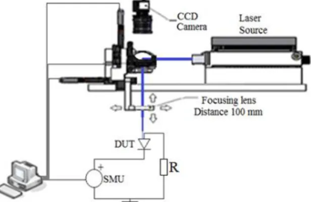
The surface of the diode is scanned by the laser beam focused by several lens in a spot of ~10µm diameter. A schematic description of the experimental bench is shown in Fig. 2. The measurement is performed in a vacuum chamber able to sustain high voltages up to 3500V. Tests have been carried out at 0 V, but also at higher voltages: 1000 V in Fig. 3 and 2350 V in Fig. 4. Near the breakdown voltage, an increase in the OBIC signal could be observed at the edge of the JTE by the side of the tip. This phenomenon is correlated with the observed luminescence due to the radiative recombination of EHPs generated by avalanche multiplication [2-3], as shown in Fig. 5.
More experimental results (including TCAD simulations) showing the variation of the OBIC signals with the applied reverse voltages will be published in the final paper. Also theoretical simulations will be used to try to estimate the concentration of active dopants.
Acknowledgments: the authors would like to thank FilSiC research program for financial support and also gratefully acknowledge Dr. Gregory GROSSET and Lionel DUPUY for the realization of test structures.
1. H. Hamad, C. Raynaud, P. Bevilacqua, S. Scharnholz, D. Planson, Materials Science Forum Vols. 821-823, pp 223-228, (2015). 2. S. Ono, M. Arai, C. Kimura, Jpn. J. Appl. Phys., vol. 43, n°. 10, pp. 7107,-7108 (2004). 3. K. Mochizuki, H. Okino, H. Matsushima, Y. Toyota, Mater. Sci. Forum, vols. 821-823, pp. 640-643 (2015). Fig. 1. Cross section of the protected bipolar PiN diode. Fig. 2. Schematic of OBIC experimental bench. Fig. 3. Top view of OBIC measurement at 1000 V. Position of the tip is deduced from the lower signal level. Fig. 4. 2D-cartography of OBIC signal vs. beam position at 2350 V (current is expressed in nA).