HAL Id: hal-01387987
https://hal.archives-ouvertes.fr/hal-01387987
Submitted on 27 Jan 2019HAL is a multi-disciplinary open access archive for the deposit and dissemination of sci-entific research documents, whether they are pub-lished or not. The documents may come from teaching and research institutions in France or abroad, or from public or private research centers.
L’archive ouverte pluridisciplinaire HAL, est destinée au dépôt et à la diffusion de documents scientifiques de niveau recherche, publiés ou non, émanant des établissements d’enseignement et de recherche français ou étrangers, des laboratoires publics ou privés.
Temperature Dependence of 4H-SiC Ionization Rates
Using Optical Beam Induced Current
Hassan Hamad, Christophe Raynaud, Pascal Bevilacqua, Sigo Scharnholz,
Dominique Planson
To cite this version:
Hassan Hamad, Christophe Raynaud, Pascal Bevilacqua, Sigo Scharnholz, Dominique Plan-son. Temperature Dependence of 4H-SiC Ionization Rates Using Optical Beam Induced Cur-rent. Materials Science Forum, Trans Tech Publications Inc., 2015, 821-823, pp.223 - 228. �10.4028/www.scientific.net/MSF.821-823.223�. �hal-01387987�
Temperature dependence of 4H-SiC ionization rates using Optical Beam
Induced Current
Hassan Hamad
1,a, Christophe Raynaud
1,b, Pascal Bevilacqua
1,c, Sigo
Scharnholz
2,d, Dominique Planson
1,e.
1Universitéde Lyon, INSA de Lyon, Laboratoire Ampère, 21 Avenue Jean Capelle, 69621 Villeurbanne
Cedex, France
2French-German Research Institute of Louis (ISL), 5 Rue du Général Cassagnou, 68301
Saint-Louis Cedex, France
a[email protected], b[email protected], c[email protected], d[email protected], e[email protected].
Keywords: 4H-SiC; bipolar diode; OBIC; multiplication coefficient; ionization rate.
Abstract. The behavior of 4H-SiC power devices in severe environment with varying temperature is a
key characteristic indicating their reliability. This paper shows the dependence of the ionization rates of 4H-SiC with respect to temperature. Optical Beam Induced Current (OBIC) measurements have been performed on PN junctions to determine the multiplication coefficient for temperature varying between 100 and 450K. That allows extracting the ionization rates by fitting the curves of multiplication coefficient.
Introduction
Silicon carbide devices become more and more used in the power electronics. Advanced studies and characterizations are needed to improve the breakdown voltage of these devices. Many optical methods are often employed to study the physical characteristics of the silicon carbide. In this paper, Optical Beam Induced Current (OBIC) method is employed to determine ionization rates for a wide temperature range going from 100 up to 450K. Ionization rates are rarely studied and the results already found are, more or less, scattered [1-5]. Their determination helps to predict more accurately the critical electric field and hence the breakdown voltage of electronic devices. OBIC method can be also used to determine carrier lifetime [6] and finally it gives an image of the electric field in the device [7].
Ionization rates
Ionization rate is defined as the number of generated charge carriers by collision per length unit from one charge carrier. The energy acquired by a charge carrier depends on the electric field. This means that ionization rates of a material depends only on material characteristics and electric field. The models that describe ionization rates are functions of electric field, they are derived by taking into account some physical approximations or empirical equations. For example, Wolff considered that the acquired energy by a charge carrier between two collisions is too much higher than the lost energy due to a collision. The distance between the two collisions is the carrier mean free path. In these conditions, he solved transport equations of Boltzmann and he obtained the expression of the ionization rates as seen in equation 1 [8]. Wolff hypothesis is applicable only for high electric field.
(
) F: electric field
The model used in this paper is the Shockley model. Shockley supposed that carriers bringing about ionization are only ones that do not undergo shocks with phonons [9]. His definition is in good agreement with the empiric formula given by Chynoweth [10] for low electric field:
(
) F: electric field
(2)
Experimental extraction of ionization rates using OBIC
Consider the reverse biased P+N junction shown in figure 1. Once it is perpendicularly illuminated with an optical beam, photon absorption and electron-hole pairs (EHPs) generation occur. An induced current can be measured. Jp is the hole current in the
N-region, Jn is the electron current in the P+
-region, JSCR is the generated current in the
space charge region (SCR), xj is the
metallurgical junction depth, xj-xp is the
SCR extension in the P+ emitter, and xn-xj is
the SCR extension in the N region. Currents obey the following equations:
( ) (3) in which Jn and Jp are algebraic quantities, q is the elementary charge and u(x) is the generation rate
by light in the SCR. The total current J = Jn + Jp is constant whatever x.
( ) (4)
( ) (5) Solutions of equations (5) and (6), with u = 0, give respectively the multiplication coefficient of electrons (Mn) and holes (Mp). Assuming that Jn(xn) >> Jp(xn) and Jp(xp) >> Jn(xp), that means it is
possible to write: Jn(xn) = Jp(xp) = J.
( ∫( ) ) ∫ ( ∫( ) ) ( ) (6)
( ) ( ∫ ( ) ) ∫ ( ∫( ) ) ( ) (7)
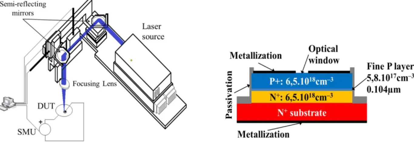
Figure 1: Schematic view of P+N junction with different regions and currents.
( )
( ) ( ∫ ( ) ) [ ∫ ( ∫( ) ) ] (8)
[ ( ∫ ( ) ) ∫ ( ∫( ) ) ] ( ∫ ( ) ) (9)
A few further steps give:
∫ ( ∫ ( ) ) (10) In the same way, we obtain:
∫ (∫ ( ) ) (11) Taking into account the generation rate u ≠ 0, solution of equations gives the total multiplication coefficient which is the ratio between the current for a given voltage V and the current for the voltage V0 for which there is no multiplication.
( ) ( ) ( ) ( ) ( ) (12) With ∫ ( ∫ ( ) ) ∫ (13) ∫ (14)
Φ and α are respectively the absorbed optical flux and the absorption coefficient of the semi-conductor. In this work, the wavelength used is 349nm, its absorption rate in the 4H-SiC is 340cm–1. So, the expression of u(x) is given by:
( ) ( ) (15) Then the photon generated current in the SCR is:
[ ( ) ( )] (16)
The minority carriers currents Jn(xp) and Jp(xn)are determined by solving the continuity equations by
taking into account the conditions on the limit [11]. From equations (2) and (12), it is possible to determine the ionization rates by fitting the experimental multiplication curve M(V) using numerical solver. In this case, the electric field distribution must be calculated in terms of the reverse voltage V.
Experimental setup
A UV pulsed laser is used to generate electron hole pairs, the wavelength of incident light is 349nm, the repetition rate can be modified between 100Hz and 5kHz (figure 2a). The pulse energy can be adjusted up to 120µJ. The pulse duration varies between 3 and 7ns according to frequency and pulse energy. An optical bench consisting of two semi-reflecting mirrors and a focusing lens is controlled with LabView to move the position (x, y and z) of the focal point. At the focal point the spot diameter is about 20µm and the beam power density is up to 100GW.cm–2. In this work, the repetition frequency is set to 1 kHz and all measurements are realized under very low pulse energy (smaller than 1 µJ/pulse). This energy is high enough to generate EHPs so an OBIC current could be measured. The studied device is placed in a vacuum chamber and its temperature is controlled. The minimum temperature is 77K due to liquid nitrogen. The laser beam passes through the window of vacuum chamber to reach the device under test. The diameter of the diode is scanned with a step of 10µm for several voltages.
Figure 2: (a) Schematic of experimental bench, (b) Cross section view of the studied diode.
To realize OBIC measurements, a circular avalanche diode similar to those described in previous studies [3] (figure 2b). The diode is realized on an N+ 4H-SiC substrate. An epitaxial P+ layer of 2.2µm thickness was grown on a fine epitaxial transition P layer of 0.104µm overlying an N+ epitaxial layer. Since the diode presents a high doping level, its breakdown voltage is very low (59V), and the peripheral protection is realized with a MESA etching. In order to allow optical beam to penetrate towards the active part of the diode, an optical window of 100×100µm2 has been performed on the metallization using SIMS technique [12].
Results and discussion
Figure 3 shows the reverse I-V characteristics of the diode for a temperature ranging from 100K up to 450K. For low voltage level, the leakage current becomes higher when the temperature increases, however the breakdown voltage increases as well.
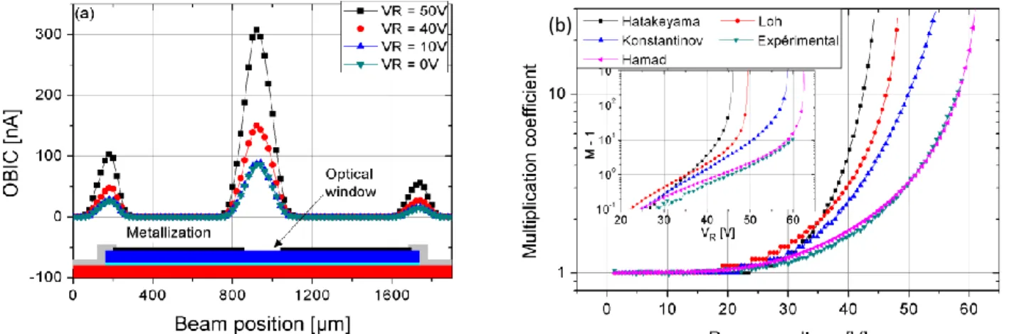
Figure 4a shows the OBIC current measured at 300K with reference to the cross section of the diode for multiple voltage levels. The current is high when laser beam illuminates the optical window. There is a weak signal when laser beam illuminates the extremity of the metallization, and it is zero everywhere else. OBIC does not change significantly for low voltages at the optical window but once approaching the breakdown voltage, it increases significantly.
For a given voltage V, the multiplication coefficient is the ratio between the current induced in the optical window and its value at 1V. Figure 4b shows experimental multiplication coefficient for this work at 300K fitted with numerical solver and compared to Konstantinov [1], Loh [4] and Hatakeyama [5] results in the same conditions. This figure reveals a significant dispersion of published multiplication coefficients between different authors.
Figure 4: (a) OBIC vs. beam position for several reverse voltages, (b) multiplication coefficient for this
work compared to others. To fit the multiplication curve, four parameters
are modified. an, bn, ap and bp give the shapes of
the ionization rates of electrons (αn) and holes
(αp). Table 1 displays the values of the values of
these parameters for temperature going from 100 to 450K. Figure 5 shows the variation of ionization rates vs. the inverse of the electric field for the same temperature range. For very low temperature (≤ 150K), αn is higher than αp.
When temperature becomes higher than about 150K, the avalanche is dominated by αp. It is
shown that αn decreases slightly when the
temperature increases. Such results have been obtained for electrons in silicon at 100, 213 and 300K [13] for lower electric field. αp increases
with the temperature up to 300K, and seems constant above 300K. At high electric field, the temperature dependence is less pronounced than
at lower electric field, as predicted by the theory [14]. Recent results by Niwa et al. [15] in SiC at T > 300K show a decrease of αp at T > 300K but for lower electric field. Therefore there is no contradiction
between our results and those of Niwa.
Figure 3: Reverse I-V characteristics for
different temperatures.
Figure 5: Ionization rates of electrons αn (empty
symbols) and of holes αp (full symbols) vs. inverse of
electric field.
Table 1: Temperature dependence of ionization rates Temperature [K] 100 150 200 250 300 350 400 450 an [106 cm-1] 0.57 0.81 1.15 1.04 0.99 0.87 0.81 1.07 bn [107 V.cm-1] 0.87 1.07 1.21 1.36 1.29 1.11 1.22 1.36 ap [106 cm-1] 1.35 1.59 1.23 1.76 1.61 1.72 1.95 1.6 bp [107 V.cm-1] 1.3 1.27 1.14 1.14 1.15 1.26 1.2 1.11 Summary
In this paper, a UV laser with appropriate power is used to generate electron hair pairs in 4H-SiC. Optical beam induced current (OBIC) is measured on an avalanche diode enabling the determination of the multiplication coefficient. The ionization rates are extracted by fitting the multiplication curves using the Shockley model. Results show that ionization rates do not vary significantly when temperature changes. A slight decrease of αn was observed when the temperature goes from 100K to
450K and a light increase of αp up to 300K. At higher temperature, αp is rather constant. These results
are obtained for high electric fields (> 3×10⁶ V.cm-1).
Acknowledgement
The authors thank the TRACE program for his financial support of this work.
References
[1] A-O. Konstantinov, Q. Wahab, N. Nordell and U. Lindefelt, Materials Science Forum, vols. 264-268, 513 (1998).
[2] R. Raghunathan and B-J. Baliga, Solid State Electronics, vol. 43, 199 (1999).
[3] D-M. Nguyen, C. Raynaud, M. Lazar, G. Pâques, S. Scharnholz, N. Dheilly, D. Tournier and D. Planson, Materials Science Forum, vols. 717-720, 545 (2012).
[4] W. Loh, B. K. Ng, J. S. Ng, S. I. Soloviev, H. Y. Cha, P. M. Sandvik, C. M. Johnson and J. P. R David, IEEE Transactions on electron devices, vol. 55, no. 8 (2008).
[5] T. Hatakeyama, T. Watanabe, T. Shinohe, K. Kojima, K. Arai, and N. Sano, Applied Physics
Letters, vol. 85, n°. 8, p. 1380-1382, 2004.
[6] T. Flohr and R. Helbig, Journal of Applied physics, vol. 66, no. 7, p. 3060 (1989).
[7] H. Hamad, P. Bevilacqua, C. Raynaud and D. Planson, 10th Conference on Ph. D. Research In Microelectronics and Electronics PRIME, (2014).
[8] P. A. Wolff, Physical Review, vol. 95, no. 6, p. 1415 (1954). [9] W. Shockley, Solid State Electronics, vol. 2, no. 1, p. 35 (1961).
[10] A. G. Chynoweth, Journal of Applied Physics, vol. 31, no. 7, p. 1161 (1960).
[11] C. Raynaud, D-M. Nguyen, N. Dheilly, D. Tournier, P. Brosselard, M. Lazar and D. Planson.
Physica status solidi A, vol. 206, n°10 (2009) p.2273-2283.
[12] M. Lazar, F. Jomard, D-M. Nguyen, C. Raynaud, G. Pâques, S. Scharnholz, D. Tournier, D. Planson, Materials Science Forum, vols. 717-720, 885 (2012).
[13] C. A. Lee R. A. Logan, R. L. Batdorf, J. J. Kleimack and W. Wiegmann, Physical Review, vol. 134, p. A761 (1964).
[14] C. R. Crowell and S. M. Sze, Applied physics letter, vol. 9, p. 242 (1966).
![Table 1: Temperature dependence of ionization rates Temperature [K] 100 150 200 250 300 350 400 450 a n [10 6 cm -1 ] 0.57 0.81 1.15 1.04 0.99 0.87 0.81 1.07 b n [10 7 V.cm -1 ] 0.87 1.07 1.21 1.36 1.29 1.11 1.22 1.36 a p [](https://thumb-eu.123doks.com/thumbv2/123doknet/14657574.553206/7.918.139.787.140.252/table-temperature-dependence-of-ionization-rates-temperature-k.webp)
