HAL Id: tel-01970171
https://tel.archives-ouvertes.fr/tel-01970171
Submitted on 31 Jan 2019
HAL is a multi-disciplinary open access
archive for the deposit and dissemination of sci-entific research documents, whether they are pub-lished or not. The documents may come from teaching and research institutions in France or abroad, or from public or private research centers.
L’archive ouverte pluridisciplinaire HAL, est destinée au dépôt et à la diffusion de documents scientifiques de niveau recherche, publiés ou non, émanant des établissements d’enseignement et de recherche français ou étrangers, des laboratoires publics ou privés.
photovoltaic systems
Pablo Arturo Fernandez Garrillo
To cite this version:
Pablo Arturo Fernandez Garrillo. Development of highly resolved and photo-modulated Kelvin probe microscopy techniques for the study of photovoltaic systems. Materials Science [cond-mat.mtrl-sci]. Université Grenoble Alpes, 2018. English. �NNT : 2018GREAY031�. �tel-01970171�
THÈSE
Pour obtenir le grade de
DOCTEUR DE LA COMMUNAUTE UNIVERSITE
GRENOBLE ALPES
Spécialité : Nanophysique
Arrêté ministériel : 25 mai 2016
Présentée par
Pablo Arturo FERNÁNDEZ GARRILLO
Thèse dirigée par Dr. Benjamin GRÉVIN,et encadrée par Dr. Łukasz BOROWIK
Préparée au sein du Laboratoire d'Électronique et de
Technologie de l'Information et de l’Institut Nanosciences et Cryogénie – CEA Grenoble
dans l'École Doctorale de Physique
Développement de techniques
de microscopie Kelvin
hautement résolues et
photo-modulées pour l'étude de
systèmes photovoltaïques
Thèse soutenue publiquement le 25 Septembre 2018, devant le jury composé de :
Dr. Sascha SADEWASSER
INL (Praga, Portugal), Examinateur
Pr. Pere ROCA i CABARROCAS
LPICM, CNRS, Ecole Polytechnique, (Paris, France), Président
Dr. Guillaume SCHULL
IPCMS DSI (Strasbourg, France), Rapporteur
Pr. Christian LOPPACHER VOIROL
IM2NP, Faculté des Sciences et Techniques, (Marseille, France) Rapporteur
Dr. Benjamin GRÉVIN
UGA, CNRS, CEA, INAC, UMR-5819 (Grenoble, France), Directeur de thèse
Dr. Łukasz BOROWIK
THESIS
To obtain the degree of
DOCTOR OF THE UNIVERSITY OF GRENOBLE
Speciality: Nanophysics
Ministerial decree: May 25, 2016
Presented by
Pablo Arturo FERNÁNDEZ GARRILLO
Thesis directed by Dr. Benjamin GRÉVIN,and supervised by Dr. Łukasz BOROWIK
Prepared at the Laboratory of Electronics and Information
Technology and the Nanoscience and Cryogenics Institute – CEA Grenoble
at the Doctoral School of Physics
Development of highly
resolved and photo-modulated
Kelvin probe microscopy
techniques for the study of
photovoltaic systems
Thesis defended publicly on September 25, 2018, in front of the Ph.D. thesis committee composed by: Dr. Sascha SADEWASSER
INL (Praga, Portugal), Member
Pr. Pere ROCA i CABARROCAS
LPICM, CNRS, Ecole Polytechnique, (Paris, France), President
Dr. Guillaume SCHULL
IPCMS DSI (Strasbourg, France), Referee
Pr. Christian LOPPACHER VOIROL
IM2NP, Faculté des Sciences et Techniques, (Marseille, France) Referee
Dr. Benjamin GRÉVIN
UGA, CNRS, CEA, INAC, UMR-5819 (Grenoble, France), Ph.D. Director
Dr. Łukasz BOROWIK
“Look deep into nature, and then you will understand everything better.” Albert Einstein
ix
This thesis is directed towards the proposition and demonstration of a set of novel advanced atomic force microscopy based techniques under ultra-high vacuum conditions, enabling to map simultaneously the surface topography and the photo-carrier dynamics at the nanometre scale. In fact, by monitoring the dependence of the average surface photo-voltage measured with Kelvin probe force microscopy, as a function of the repetition frequency of a modulated excitation source, we will access the built-up and decay dynamics of the surface photo-voltage response which in turn will allows us to study the photo-carrier dynamics over a wide range of samples. In order to enable the 2-dimensional nano-imaging process, Kelvin probe force microscopy under modulated illumination measurements are acquired repeatedly over each point of a predefined grid area over the sample acquiring a set of spectroscopy curves. Then, using an automatic mathematical fit procedure, spectroscopy curves are translated into pixels of the photo-carrier dynamic time-constant images.
Moreover, these set of novel techniques will be used to investigate the surface photo-voltage dynamics in several kinds of photovoltaic samples from different technological branches such as small grain polycrystalline silicon thin films, silicon nanocrystal-based third generation cells, bulk heterojunction donor-acceptor organic photovoltaics and organic-inorganic hybrid perovskite single crystal cells, discussing in each case the photo-carrier recombination process and its relation with the material’s structuration/morphology. Finally, technical aspects of these novel techniques will be discussed as well as their limitations and remaining open questions regarding results interpretation.
xi
Cette thèse propose, décrit et utilise un ensemble de techniques basées sur la microscopie à force atomique sous ultravide pour la cartographie simultanée, à l'échelle nanométrique, de la topographie de surface et des dynamiques temporelles des photo-porteurs. Ainsi, en contrôlant la dépendance du photo-potentiel de surface moyen mesuré par microscopie à force de sonde Kelvin en fonction de la fréquence de répétition d'une source lumineuse externe d'excitation, le dispositif expérimental permet d’accéder aux dynamiques temporelles du photo-potentiel de surface qui, à leur tour, permettent d'étudier les dynamiques des photo-porteurs sur une large gamme d'échantillons. Afin de permettre le processus de nano-imagerie bidimensionnelle, ces mesures sont acquises de manière répétée en enregistrant des courbes spectroscopiques en chaque point d’une grille prédéfinie. En utilisant une procédure d'ajustement mathématique automatique, les dynamiques temporelles des photo-porteurs sont extraites à partir des données expérimentales.
Cet ensemble de nouvelles méthodes est utilisé pour l’étude de plusieurs types d'échantillons issus de différentes technologies photovoltaïques telles que des couches minces en silicium poly-cristallin à petits grains, des cellules de troisième génération à nano cristaux de silicium, des cellules photovoltaïques organiques et des cellules à base de matériaux de structure pérovskite. Dans chaque cas, on décrit les processus de recombinaison des photo-porteurs ainsi que leur lien avec la morphologie et la structuration du matériau. Enfin, les aspects techniques de ces nouvelles méthodes d’analyse sont présentés, ainsi que leurs limites, notamment celles concernant l'interprétation des résultats.
xiii
Abstract ... ix
Résumé ... xi
Contents ... xiii
List of Figures ... xvii
Notations ... xxi 1 | Introduction ... 1 1.1 Thesis Outline ... 8 References ... 10 2 | Photovoltaics ... 13 2.1 Context ... 13
2.2Physics of classic solar cells: The case of silicon and other inorganic photovoltaics technologies ... 16 2.3Organic photovoltaics ... 26 2.4Perovskite photovoltaics ... 32 2.5Characterization methods ... 35 Conclusion ... 37 References ... 39
3 | Scanning probe microscopy techniques ... 45
3.1 Context ... 46
3.2 Nanotechnology ... 46
3.3 Atomic force microscopy ... 47
3.3.4Tip-sample interaction forces ... 58
3.4Kelvin probe force microscopy ... 64
3.4.1Amplitude modulation Kelvin probe force microscopy ... 68
3.4.2Frequency modulation Kelvin probe force microscopy ... 69
3.4.3Kelvin probe force spectroscopy ... 70
3.5Calibrated work function mapping by Kelvin probe force microscopy... 71
3.5.1Highly oriented pyrolytic graphite: A work function reference sample? ... 73
3.5.2An alternative work function calibration protocol ... 75
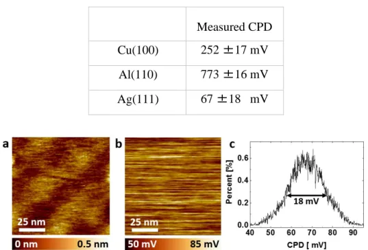
3.5.3Absolute work function measurements: Comparison against theoretical values and achievable lateral resolution ... 81
3.6Employed scanning probe microscopy setups ... 84
Conclusion ... 90
References ... 91
4 | Frequency modulated illumination Kelvin probe force microscopy ... 99
4.1 Context ... 99
4.2 Frequency modulated illumination Kelvin probe force microscopy investigations .... 103
4.2.1 Silicon based photovoltaics ... 107
4.2.2Bulk heterojunction donor-acceptor organic photovoltaics ... 115
4.2.3Spectroscopic and time-resolved measurements over perovskite photovoltaics .. 131
Conclusion ... 142
References ... 143
5 | Plausible sources of artefacts in frequency modulated illumination Kelvin probe force microscopy and how to avoid them ... 147
5.1 Context ... 147
5.2 Capacitance artefacts ... 149
5.3 Comparing amplitude modulation and frequency modulation Kelvin probe force microscopy modes ... 156
5.4 Frequency mixing ... 157
5.5 Other sources of artefacts ... 159
5.6 An improved protocol for photo-carriers dynamics investigation ... 160
xv
6 | Towards the numerical analysis of spectroscopy curves ... 181
6.1 Context ... 181
6.2 The need for numerical simulations ... 183
6.2.1 SPECTY ... 184
6.3 Numerical simulations on a silicon nanocrystal solar cell ... 187
6.4 Organic photovoltaics: Mathematical fit versus numerical analysis. ... 192
Conclusion ... 196
References ... 197
7 | Conclusion ... 199
8 | Appendix ... 203
8.1 Additional photo-carrier dynamic results over the cross section of epitaxial silicon solar cell ... 203
8.2 Correcting the fitting functions from the capacitance effects ... 207
References ... 213
Publications ... 215
Patent Application ... 217
Conferences & Seminars... 219
xvii
Figure 1.1– Yearly temperature anomalies from 1880 to 2014 ... 2
Figure 1.2– Global PV modules price trend 2009-2016 ... 3
Figure 1.3– Research solar cell efficiency records ... 4
Figure 1.4– Textile-based organic photovoltaic integrated with clothing ... 5
Figure 2.1– Band gap schematic ... 18
Figure 2.2– Recombination mechanisms in inorganic semiconductors... 19
Figure 2.3– Photon absorption in direct and indirect bandgap semiconductors ... 20
Figure 2.4– p-n junction schematic ... 22
Figure 2.5– Hybridization for the case of ethene (C2H4) ... 27
Figure 2.6– Structure of organic photovoltaic devices ... 29
Figure 2.7– Major steps of charge generation and recombination... 30
Figure 2.8– Structure of perovskites photovoltaic devices ... 33
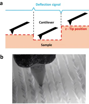
Figure 3.1– AFM cantilever ... 49
Figure 3.2– Schematics of an optical-beam AFM cantilever deflection system ... 49
Figure 3.3– Contact AFM operation mode depiction ... 50
Figure 3.4– Approach-retract curve (force curve) ... 51
Figure 3.5– AFM amplitude modulation operation mode depiction ... 53
Figure 3.6– AFM frequency modulation operation mode depiction ... 54
Figure 3.7– FM-AFM simplified functioning system scheme... 58
Figure 3.8– Total tip-sample interaction force over tip-sample distance z ... 59
Figure 3.9– CPD measuring principle with KPFM ... 67
Figure 3.10– Schematic of KPFM and its feedback system ... 70
Figure 3.11– Kelvin parabola of the frequency-shift as a function of a static bias ... 71
Figure 3.12– Topography and CPD images on HOPG by FM-KPFM. ... 74
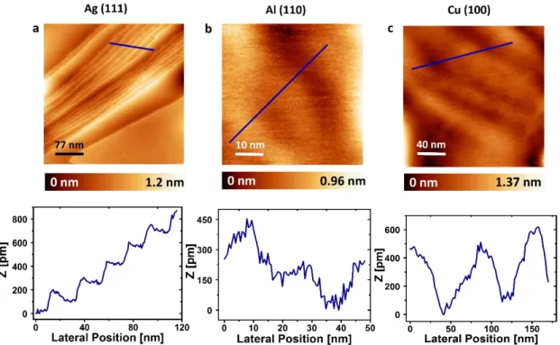
Figure 3.13– Topography images and corresponding cross section profiles of samples... 78
xviii
sample ... 83
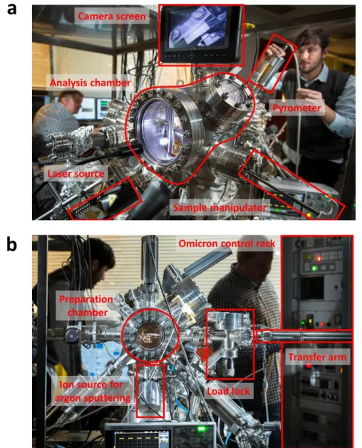
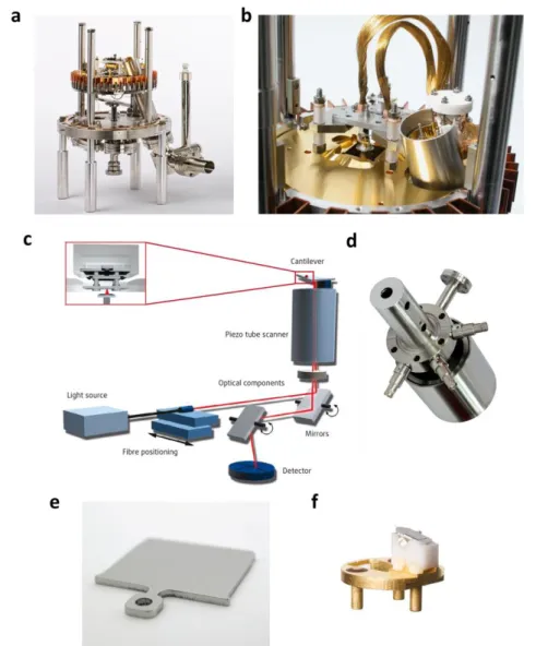
Figure 3.17– LETI’s Omicron UHV VT AFM system... 85
Figure 3.18– VT-AFM system from Scienta Omicron ... 86
Figure 3.19– INAC’s Omicron UHV VT AFM system ... 87
Figure 3.20– Multiple wavelengths laser source ... 88
Figure 3.21– Backside illumination sample holder ... 89
Figure 3.22– Arbitrary waveform generator Keysight 33622A ... 89
Figure 4.1– Illustration of the evolution of the surface photovoltage under modulated illumination as a function of time ... 102
Figure 4.2– Schematic illustration of FMI-KPFM. ... 104
Figure 4.3– 2-dimensional spectroscopy data acquisition. ... 106
Figure 4.4– Spectroscopic approach depiction ... 108
Figure 4.5– Schematic illustrations of the energy band diagrams for the n-doped silicon substrate (n-Si) and the poly-crystalline silicon thin film (poly-Si) ... 110
Figure 4.6– Results over the poly-Si film sample... 111
Figure 4.7–Description of the SiNC embedded in 30 nm of SiO2 sample ... 112
Figure 4.8– Results over the SiNC embedded in 30 nm of SiO2 sample ... 114
Figure 4.9– FMI-KPFM investigations on back side geometry configuration over an organic photovoltaic sample ... 117
Figure 4.10– FMI-KPFM investigations on back side geometry configuration over an organic photovoltaic sample (zoomed in) ... 119
Figure 4.11– FMI-KPFM at different illumination intensities. ... 121
Figure 4.12– Average potential as a function of the modulation illumination frequency acquired over the nanophase segregated PDBS-TQx/PC71BM blend ... 123
Figure 4.13– Case of a single SPV component characterized by a built up and a decay time ... 125
Figure 4.14– Case of two different SPV component characterized by different built up and a decay times... 126
Figure 4.15– Average potential as a function of the modulation illumination frequency acquired over the nanophase segregated PDBS-TQx/PC71BM blend (fitted) ... 127
Figure 4.16– Results over the nanophase segregated PDBS-TQx/PC71BM blend ... 129
Figure 4.17– Spectroscopic curves acquired for different illumination conditions on the nanophase segregated PDBS-TQx/PC71BM blend ... 131
xix
Figure 4.19– Description of the p-type MAPbBr3 sample ... 137
Figure 4.20– Resutls over the MAPbBr3 sample ... 138
Figure 4.21– MAPbBr3 sample evolution ... 139
Figure 4.22– Topography and surface potential images of the UHV cleaved sample after several hours under illumination at 2.8 mW/cm2 ... 140
Figure 4.23– Topography, SPV decay time, dynamic SPV and SP at 990 Hz images of the UHV cleaved sample respectively. ... 141
Figure 5.1– Scheme showing how photo-excited charges modify the effective distance between capacitor plates... 149
Figure 5.2– Schematic illustration of Kelvin probe force spectroscopy under modulated illumination ... 151
Figure 5.3– Results of Kelvin probe force spectroscopy under modulated illumination ... 152
Figure 5.4– Graphical comparison of both measured and simulated CPD as a function of the illumination modulation frequency ... 154
Figure 5.5– FMI-KPFM in AM-KPFM mode against FM-KPFM mode ... 156
Figure 5.6– Improve FMI-KPFM protocol depiction. ... 160
Figure 5.7– Results of the implementation of the improved FMI-KPFM protocol in single-point mode ... 161
Figure 5.8– Improved FMI-KPFM protocol results ... 164
Figure 5.9– Corrected SPV decay image ... 166
Figure 5.10– Open loop mode against close loop mode. ... 167
Figure 5.11– Single-points FMI-KPFM measurements taken at different illumination intensities. ... 170
Figure 5.12– SPV under continuous wave illumination as a function of the illumination intensity. ... 170
Figure 5.13– Numerical simulation showing a SPV made up of two different components contributions with inverted polarities and different dynamics ... 171
Figure 5.14– Unveiling the dual polarity SPV behavior. ... 173
Figure 5.15– FMI-KPFM self-consistency check up ... 176
Figure 5.16– Image of 𝑑2𝐶𝑑𝑧2 under continuous wave illumination and in dark conditions obtained via the FMI-KPFM improved protocol. ... 177
Figure 6.1– Physical description of simulation parameters. ... 185
Figure 6.2– SPECTY working principle ... 186
xx
τ𝑏 =10 µs and τ𝑏 =20 µs respectively ... 190
Figure 6.5– Simulated-SPV as a function of time for different excitation modulation frequencies ... 191
Figure 6.6– Simulated-SPVAV as a function of the number of excitation cycles for different excitation modulation frequencies ... 192
Figure 6.7– CPD data obtained from the implementation of the improved FMI-KPFM protocol ... 194
Figure 6.8– Comparison between curves: Mathematical fits and simulated SPVAV curve ... 195
Figure 8.1– Cross section of epitaxial silicon solar cell ... 204
Figure 8.2– Results over the cross section of epitaxial silicon solar cell ... 205
Figure 8.3– Different calculation scenarios ... 208
xxi
Notations
AFM Atomic Force Microscopy
AM Amplitude Modulation
BHJ Bulk Heterojunction
CPD Contact Potential Difference
CT Charge Transfer
CTS Charge Transfer State
DA Donor-Acceptor
FF-trEFM Fast Free Time-Resolved Electrostatic Force Microscopy
FM Frequency Modulation
FMI-KPFM Frequency-Modulated Illumination Kelvin Probe Force Microscopy HOMO Highest Occupied Molecular Orbital
HOPG Highly Oriented Pyrolitic Graphite
ITO Indium Tin Oxide
KPFM Kelvin Probe Force Microscopy
LCAO Linear Combination of Atomic Orbitals (method)
LR Long Range
LUMO Lowest Unoccupied Molecular Orbital
OPV Organic Photovoltaic (cell)
PLL Phase-Locked Loop
PSD Photo Sensitive Diode
PV Photovoltaic (cell)
P3HT Poly(3-Hexylthiophene)
PC71BM [6,6]-Phenyl-C71-Butyric Acid Methyl Ester QSSPC Quasi-Steady-State Photo-Conductance
SEM Scanning Electron Microscopy
xxii
SR Short Range
SSS Silicon Super Sharp (cantilever)
STM Scanning Tunneling Microscopy
TEM Transmission Electron Microscopy
TiOx Titanium Oxide
trEFM Time-Resolved Electrostatic Force Microscopy
UHV Ultra High Vacuum
vdW van der Waals
WF Work Function
VT Variable Temperature
Γ 2nd harmonic signal from the lock-in detection.
A Cantilever Amplitude
BEX Exciton Binding Energy
BECTS Charge Transfer State Binding Energy
C Capacitance
CIGS Copper Indium Gallium (Di)Selenide
∆f Frequency Shift
∆f 0 Frequency Shift Setpoint
EF Fermi Energy
Egap Semiconductor Bandgap Energy
Evac Vacuum Energy
f 0 (First) Cantilever Resonance Frequency
f K Kelvin Modulation Frequency
𝑭𝟐𝒘 Second Harmonic Component of the Electrostatic Force
Fel Electrostatic Force
Fint (Total) Tip-Sample Interaction Force
FSR Short-Range Force
xxiii
FF Fill Factor
H Hamaker Constant
k Cantilever Spring Constant
Φ Work Function
Q Quality Factor
R Tip Radius
RMS Root Mean Square (of surface roughness)
τd Surface Photo-Voltage Decay TimeConstant
τb Surface Photo-Voltage Built-Up TimeConstant
T Temperature
µW-PCD Microwave Photo-Conductivity Decay
V Voltage
VAC Alternating Current Modulation Bias
VAV Average Surface Photo-Voltage
VI Surface Photo-Voltage Under Illumination
VD Surface Photo-Voltage in Dark
VDC Kelvin Compensation Bias
VOC Open Circuit Voltage
Content
1.1Thesis Outline ... 8
References ... 10
Most governments around the world, as well as the scientific community have agreed that in order to prevent catastrophic climate change, global warming must remain under 2°C with respect to pre-industrial mean temperatures.[1] However, the mean global temperature has already risen by 0.8°C since 1880, with two-thirds of the warming occurring since 1975, at a rate of roughly 0.15-0.20°C per decade.[2] Figure 1.1 shows yearly temperature anomalies from 1880 to 2014 as recorded by the United States of America (USA) national aeronautics and space administration (NASA), the USA national oceanic and atmospheric administration (NOAA), the Japan meteorological agency, and the British met office Hadley centre.[3] All data sources show an increasingly fast warming in the past few decades, being the last decade the warmest. In December 2015, at the United Nations climate change conference (COP 21) in Paris, governments acknowledged the increasing threat of climate change and agreed to work together towards keeping global warming to 1.5°C at most. However, society is already facing extreme weather conditions. From dangerous storms and floods, to heatwaves and droughts, extreme weather events are increasing in frequency and intensity.[1]
At the same time, world population increases at a rate of approximately 1.1% per year. Currently there are over 7.4 billion humans living on earth, and world population is expected to reach 10 billion by mid-2050.[4] This growth in population translates into an increasing energy demand that cannot be satisfied with fossil fuels in the long term, not only because of its negative impact on climate change but also for it is a limited resource.
Our dependence on fossil energy is polluting air, increasing the spread of disease and making water supplies scarcer and less safe.[1] Urgent action is needed to reduce carbon
emissions if dangerous climate change is to be avoided. The vast majority of fossil fuels, which are the biggest driver of climate change,[5] have to be left in the ground, to have a chance of preventing dangerous global warming. But at the same time, the energy demand of an increasing population has to be attended.
Figure 1.1– The line plot below shows yearly temperature anomalies from 1880 to 2014 as recorded by NASA, NOAA, the Japan Meteorological Agency, and the Met Office Hadley Centre (United Kingdom).
From Ref. [3]
Fortunately, renewable energy alternatives are growing rapidly and are more competitive than ever. Among the different renewable energy sources, the sun is arguably the most abundant clean source of energy that is capable of enabling sustainable economic growth, with minimum detrimental impact on the environment.[6] To emphasize this, it if often alleged that sunlight received by earth in one hour is enough to meet the annual energy needs of the current worldwide population.[7]
Solar power, once so expensive it only made economic sense in spacecraft, is becoming affordable enough that it is anticipated to drive coal and natural-gas plants out of business earlier than previously forecasted. Indeed, solar modules costs have steadily halved every 10
years since 1976 following Swanson’s law[8] prediction, currently modules prices for several PV technologies are well below 1$ per Watt in most Earth locations as shown in Figure 1.2. Moreover, while prices are dropping, solar energy generation is increasing. In 2016, new solar photovoltaic capacity around the world grew by 50% according to the International Energy Agency.[9]
Figure 1.2– Global PV modules price trend 2009-2016. Data from Ref. [10]
To date, photovoltaic (PV) technology stands out as the only renewable energy option that: i) generates electricity without moving parts, ii) is practical for small and large scale applications, iii) is suitable for the urban environment as well as remote applications, iv) is silent, v) is a very low-maintenance technology and vi) has a low ‘embodied energy’, meaning the amount of energy invested in making PV modules is relatively small, although this can largely vary depending on the technology.
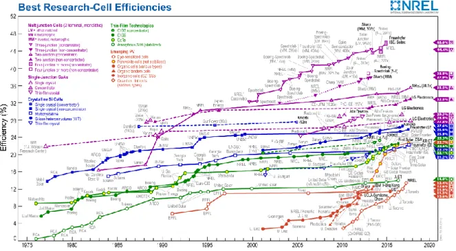
Most of today’s installed photovoltaic panels are single junction cells based on monocrystalline silicon.[11] Monocrystalline silicon solar cells have been continuously progressing in efficiency and decreasing fabrication cost over the last half decade.[12, 13] Monocrystalline silicon cells with efficiencies of up to 26.6%[14] have already been attained, which already accounts for more than 70% of the theoretically achievable performance. As
mentioned before, nowadays, they are capable of generating electricity at a comparable cost to the price of electricity generated from fossil fuels in some parts of the world.[15] However, there are many other newer and promising PV technologies with lower fabrication costs and continuously increasing efficiencies as shown in Figure 1.3. Many of them rely on the use of thin films of poly/multi-crystalline or nano-structured materials, or on materials displaying a heterogeneous morphology at the mesoscopic or nanoscopic scale.
Figure 1.3– Research solar cell efficiency records confirmed and published by the National Renewable Energy Laboratory. From Ref. [14]
Multi-crystalline solar cells, which have the advantage of being fabricated without the high cost generated by the Czochralski crystal growth process,[16] have already achieve efficiencies of up to 22.3%.[14] Thin layer solar cells of copper indium gallium selenide (CIGS) and cadmium telluride (CdTe) have been developed at reduced costs and show efficiencies of up to 22.6%.[14] The highest efficiency so far, with values of 46% has been achieved by multi-junction solar cells based on an indium gallium phosphide/gallium arsenide/indium gallium arsenide structure (InGaP/GaAs/InGaAs).[12] Organic photovoltaic (OPV) systems, based on organic π-conjugated materials create a promising complementary
branch in view of silicon technologies[11] and recently efficiencies of 13.1% have been reached.[17] Besides such relatively high performances, OPV cells also offer numerous advantages compared to inorganic solar cells. In contrast to the latter, they can be produced without any energy-intensive manufacturing process. Furthermore, these OPV cells are lightweight and can potentially be constructed on flexible substrates offering possibilities for new applications like the integration in mobile devices, buildings and even in clothes as shown in Figure 1.4.[11, 18]
Figure 1.4– (a) Concept of a stitchable OPV on textile electrode. (b) Textile-based organic photovoltaic integrated with clothing. From Ref. [18]
In the emerging field of hybrid perovskites solar cells, efficiencies of up to 22.7%[14] have been reached. These cells can be manufactured with simple wet chemistry techniques in a traditional laboratory environment with the potential to be scaled up with relative feasibility.[6, 19] There is a growing interest in this technology as it promises to break the prevailing PV paradigm by combining both ultimately low cost and high efficiency.[6]
For these emerging PV technologies, it is crucial to fully understand the complex interplay between the nanostructure and photo-transport mechanisms. Indeed, the investigation of PV devices under operation conditions at the nanometer scale can give us valuable information about processes that occur at a scale of the order of tens and hundreds of nanometers, such as exciton dissociation, carrier transport across the material and carrier recombination. Undeniably, fundamental understanding of structure property relations in
energy materials and devices on the mesoscopic and nanoscopic levels is prerequisite to knowledge-driven design and optimization as well as to increase the commercial competitiveness of these technologies.
Indeed, the local investigation of certain PV characterization parameters, plays an important role in the ongoing performance improvement process. For instance, the work function (WF), which is the minimum energy needed to remove an electron to a point in the vacuum immediately outside of the surface (see Chapter 3) has a significant importance in the field of photovoltaics as it influence the band line-up at the interface between organic or perovskite materials and the electrodes of the PV device,[20, 21] hence its local study is of upmost importance when it comes to minimize sources of losses and maximize charge collection. [21-23]
Indeed, identifying the mechanisms of loss is at the core of the ongoing quest for increasing PV performances, as well as quantifying the role of heterogeneities on the recombination at the nanoscale. As we well see, photo-carrier lifetime is a parameter of paramount importance in the overall efficiency of a solar cell as it defines the proportion of photo-generated charges collected at the electrodes.
To date, most experimental approaches developed to probe recombination dynamics and hence carrier lifetime, focus on the use of methods such as transient photo-voltage[24], charge extraction[25], microwave photo-conductivity decay (µW-PCD)[26] and quasi-steady-state photo-conductance (QSSPC).[27] Yet, these techniques average out sample properties over macroscopic scales, rendering them unsuitable for directly assessing the influence of the nanostructure and local defects on photo-carrier dynamics.
In order to overcome this, few teams started to develop time-resolved scanning probe microscopies focused in addressing photo-carrier dynamics at the nanoscale.[28] In this context, Kelvin Probe Force Microscopy (KPFM)[29] under frequency modulated illumination arises as an alternative in photo-carrier dynamics measurements, as it has been used to probe the recombination dynamics in organic[28, 30] and the minority carrier lifetime in inorganic
semiconductors.[31, 32] However, for the most part, time-resolved KPFM-based methods have only been applied to obtain information coming from single points of the sample.
In that context, the focus of this thesis is directed towards the proposition and demonstration of a set of novel advanced atomic force microscopy (AFM)[33] based techniques under ultra-high vacuum (UHV) conditions, enabling to map simultaneously the surface topography at the nanometre scale and the photo-carrier dynamics with a temporal resolution covering 9 decades, from the nanosecond to the second scales (see Chapter 4). In particular, the technique covering the nanosecond to the millisecond range consist in monitoring the dependence of the average surface photo-voltage (SPV) measured with KPFM, as a function of the repetition frequency of a modulated excitation source. This process is repeated over each point of a predefined grid area over the sample enabling the 2-dimensional nano-imaging process of the photo-carrier dynamics.
After a brief but concise description of the employed scanning probe microscopy techniques, where special attention is given to describe the basic principle behind KPFM and WF measurements (see Chapter 3), in Chapter 4 KPFM under frequency-modulated illumination (FMI-KPFM) is used to investigate the SPV dynamics in several kinds of PV samples from different technological branches ranging from small grain polycrystalline silicon thin film and silicon nanocrystal-based third generation cells, to bulk heterojunction (BHJ) donor-acceptor (DA) OPV and organic-inorganic hybrid perovskite single crystal cells, giving in each case special attention to the photo-carrier recombination process and its relation with the material’s structuration/morphology.
Chapter 5 will be a FMI-KPFM technical chapter devoted to the introduction of plausible artefacts sources and guidelines to diminish their influence on measurements.
Finally, in Chapter 6 an automatic numerical simulation routine that enables to predict
the behaviour of spectroscopy curves of the average surface photovoltage as a function of a frequency-modulated excitation source in photovoltaic materials, is used to compare simulated and FMI-KPFM experimental results. In this chapter it is also shown how this simulation
routine can complement experimental results as additional information about the sample’s photo-carriers dynamics can be gained via the numerical analysis.
1.1 Thesis Outline
In the following, a short outline of this thesis will be presented:
In Chapter 2 the basics of inorganic organic and hybrid photovoltaics will be introduced including all elements needed for the discussion of the experimental results. In this chapter an insightful overview of several emerging photovoltaic technologies will be given, paying special attention to their possible forthcoming role in the PV market. The importance of nano-characterization for the development of different emerging PV technologies will be also highlighted in this chapter.
As mentioned above, Chapter 3 will give a summarized description of the employed scanning probe microscopy techniques as well as the used UHV AFM systems. Here, special attention is given to describe the basic principle behind KPFM and WF measurements highlighting its importance in the field of photovoltaics. To better illustrate KPFM working principle, in this chapter, an original WF calibration procedure for KPFM probes under UHV using monocrystalline metallic materials with known crystallographic orientation is proposed and demonstrated.
Chapter 4 will introduce the conception and implementation of a novel KPFM-based technique (FMI-KPFM) that allows the acquisition of SPV dynamics images, with a sub-10 nm lateral resolution. Small grain polycrystalline silicon thin films, silicon nanocrystal-based third generation cells, organic donor-acceptor blends and organic-inorganic hybrid perovskite single crystal cells will be used as samples. For each sample, the discussion will be focus on the photo-carrier recombination process and its relation with the material’s structuration/morphology.
Chapter 5 will be focused on the discussion of plausible sources of artefacts in FMI-KPFM measurements, such as capacitance and resonant-induced effects. An improved measurement protocol will be introduced, aiming at avoiding or diminishing these effects.
In Chapter 6 insights on FMI-KPFM data treatment are given. Here, special attention is given to the development of an automatic numerical simulation routine that enables to compare simulated and KPFM experimental results. It is show how experimental FMI-KPFM results are confirmed by the numerical analysis and how additional information about the photo-carriers dynamics can be found via this simulation routine.
The conclusion in Chapter 7 will summarize the thesis, discuss current projects and describe future perspectives.
References
1. Nature, W.W.F.F. Climate & Energy. 2017; Available from: http://wwf.panda.org/what_we_do/footprint/climate_carbon_energy/.
2. Hansen, J., et al., Global Surface Temperature Change. Reviews of Geophysics, 2010.
48(4).
3. Observatory, N.E. Global Temperatures. 2014; Available from: https://earthobservatory.nasa.gov/Features/WorldOfChange/decadaltemp.php.
4. United Nations, D.o.E.a.S.A., Population Division, World Population Prospects: The
2017 Revision, Methodology of the United Nations Population Estimates and Projections. 2017: New York: United Nations.
5. Change, I.P.o.C., IPCC, 2014: Climate Change 2014: Synthesis Report. Contribution
of Working Groups I, II and III to the Fifth Assessment Report of the Intergovernmental Panel on Climate Change 2014, Intergovermental Panel on Climate Change: Geneva,
Switzerland. p. 151.
6. Snaith, H.J., Perovskites: The Emergence of a New Era for Low-Cost, High-Efficiency
Solar Cells. The Journal of Physical Chemistry Letters, 2013. 4(21): p. 3623-3630.
7. Morton, O., A new day dawning?: Silicon Valley sunrise. Nature, 2006. 443: p. 19. 8. Carr, G., Sunny uplands. The Economist, 2012.
9. Agency, I.E., Renewables 2017: Analysis and Forecasts to 2022. Market Report Series. 2017: International Energy Agency.
10. Agency, I.R.E. Solar PV Costs 2010-2015. 2015; Available from: http://resourceirena.irena.org/gateway/dashboard/?topic=3&subTopic=32.
11. Fuchs, F., Model Donor-Acceptor Systems for Organic Photovoltaics Investigated by
Scanning Probe Microscopy, in Physics. 2014, Université Grenoble Alpes: Grenoble.
12. Green, M.A., et al., Solar cell efficiency tables (version 40). Progress in Photovoltaics: Research and Applications, 2012. 20(5): p. 606-614.
13. Green, M.A., Silicon solar cells: evolution, high-efficiency design and efficiency
enhancements. Semiconductor Science and Technology, 1993. 8(1): p. 1.
14. Laboratory, N.R.E. Best Research-Cell Efficiencies. 2017; Available from: https://www.nrel.gov/pv/assets/images/efficiency-chart.png.
15. Branker, K., M.J.M. Pathak, and J.M. Pearce, A review of solar photovoltaic levelized
cost of electricity. Renewable and Sustainable Energy Reviews, 2011. 15(9): p.
4470-4482.
16. Brown, R.A., Theory of transport processes in single crystal growth from the melt. AIChE Journal, 1988. 34(6): p. 881-911.
17. Zhao, W., et al., Molecular Optimization Enables over 13% Efficiency in Organic Solar
Cells. Journal of the American Chemical Society, 2017. 139(21): p. 7148-7151.
18. Lee, S., et al., Stitchable organic photovoltaic cells with textile electrodes. Nano Energy, 2014. 9: p. 88-93.
19. Saidaminov, M.I., et al., High-quality bulk hybrid perovskite single crystals within
minutes by inverse temperature crystallization. Nature Communications, 2015. 6: p.
7586.
20. Brabec, C.J., Organic photovoltaics: technology and market. Solar Energy Materials and Solar Cells, 2004. 83(2): p. 273-292.
21. Stratakis, E., et al., Improving the efficiency of organic photovoltaics by tuning the work
function of graphene oxide hole transporting layers. Nanoscale, 2014. 6(12): p.
6925-6931.
22. Kim, J.S., et al., Control of the electrode work function and active layer morphology
via surface modification of indium tin oxide for high efficiency organic photovoltaics.
Applied Physics Letters, 2007. 91(11): p. 112111.
23. Worfolk, B.J., et al., Work Function Control of Interfacial Buffer Layers for Efficient
and Air-Stable Inverted Low-Bandgap Organic Photovoltaics. Advanced Energy
Materials, 2012. 2(3): p. 361-368.
24. McNeill, C.R., I. Hwang, and N.C. Greenham, Photocurrent transients in all-polymer
solar cells: Trapping and detrapping effects. Journal of Applied Physics, 2009. 106(2):
p. 024507.
25. Hanfland, R., et al., The physical meaning of charge extraction by linearly increasing
voltage transients from organic solar cells. Applied Physics Letters, 2013. 103(6): p.
063904.
26. Ahrenkiel, R.K. and S. Johnston, Contactless measurement of recombination lifetime
in photovoltaic materials. Solar Energy Materials and Solar Cells, 1998. 55(1): p.
59-73.
27. Sinton, R.A. and A. Cuevas, Contactless determination of current–voltage
characteristics and minority‐carrier lifetimes in semiconductors from quasi‐steady‐ state photoconductance data. Applied Physics Letters, 1996. 69(17): p. 2510-2512.
28. Cox, P.A., et al., Imaging Charge Transfer State Excitations in Polymer/Fullerene
Solar Cells with Time-Resolved Electrostatic Force Microscopy. The Journal of
Physical Chemistry Letters, 2015. 6(15): p. 2852-2858.
29. Nonnenmacher, M., M.P. O’Boyle, and H.K. Wickramasinghe, Kelvin probe force
microscopy. Applied Physics Letters, 1991. 58(25): p. 2921-2923.
30. Shao, G., et al., Intensity-Modulated Scanning Kelvin Probe Microscopy for Probing
31. Takihara, M., T. Takahashi, and T. Ujihara, Minority carrier lifetime in polycrystalline
silicon solar cells studied by photoassisted Kelvin probe force microscopy. Applied
Physics Letters, 2008. 93(2): p. 021902.
32. Borowik Ł., L.H., Chevalier N., Mariolle D., Renault O., Measuring the lifetime of
silicon nanocrystal solar cell photo-carriers by using Kelvin probe force microscopy and x-ray photoelectron spectroscopy. Nanotechnology, 2014. 25(26): p. 265703.
33. Binnig, G., C.F. Quate, and C. Gerber, Atomic Force Microscope. Physical Review Letters, 1986. 56(9): p. 930-933.
Content
2.1 Context ... 13
2.2Physics of classic solar cells: The case of silicon and other inorganic photovoltaics technologies ... 16 2.3Organic photovoltaics ... 26 2.4Perovskite photovoltaics ... 32 2.5Characterization methods ... 35 Conclusion ... 37 References ... 39
Ce chapitre a pour objectif d'introduire les bases du composant photovoltaïque en matériau inorganique organique et hybride, tout en incluant tous les éléments nécessaires pour l’analyse des résultats expérimentaux. Notamment, un aperçu approfondi de plusieurs technologies émergentes est présenté, en accordant une attention particulière à leur éventuel rôle dans le développement futur des composants pour le photovoltaïque. L'importance de la nano-caractérisation pour le développement de ces dispositifs est également soulignée dans ce chapitre.
2.1 Context
About 4.5-billion years ago, in the wide vastness of space, gravity, one of the fundamental forces of nature, drew the remnants from the violent death of previous stars along with gas and dust together to create a protostar that would eventually become our Sun.[1] This young protostar was basically a giant ball of hydrogen and helium. Few tens of millions years later, the temperature and pressure inside this protostar increased, jumpstarting the hydrogen’s
nuclear fusion process that drives the Sun nowadays (i.e., turning hydrogen into helium). Fast-forward to the future and we will see that in approximately 5-billion years the sun will run out of hydrogen in its core,[2] from that point on, gravity will compress the start which in turn will increase the temperature and pressure until the point where helium is able to fuse into carbon. The energy produced by the helium fusion will cause the Sun to expand outwards many times its current size and become a red giant.[3] While there is still a scientific debate around whether our planet will be engulfed by the Sun’s expansion or whether it will orbit dangerously close to the dimmer star, either way, life as we know it on Earth will cease to exist. Fast-forward 1-billion years more into the future and we will witness the Sun’s shrinking back down to become a white dwarf, at this point, the life-giving light will slowly dissipate.[2, 4]
However, in the meantime, the Sun has been the source of all of the energy that drives biological and physical processes on Earth. The Sun is responsible for the appearance of life on Earth, as every known life form uses solar energy in some way to sustain itself.
Since the dawn of humankind solar energy has been vital for survival. Aboriginal cultures used the Sun's energy for crucial activities such as heating their dwellings and curing their nourishment.[5] Solar energy played a very important role in these cultures as many of them even worshiped and revered the Sun. As ages passed, more complex ways of capturing the energy irradiated by the sun were developed. Already in 1200 A.D. in the America's, the Anasazi tribe incorporated passive solar design in their cliff dwellings that captured the winter sun to warm their homes.[6] As cultures developed, some even created laws related to accessing solar energy. In the ancient Roman Empire it was forbidden by the law to build a dwelling that blocked the Sun from their neighbour’s home. Indeed, the Roman law enforced solar rights as an important source of light and heat.[7]
However, it was not until 1883, when C. E. Fritts, developed the first device which enabled the direct conversion of light into electricity.[8] It consisted of a thin sheet of selenium melted on a metal substrate and covered with a silver film. A few more decades will pass before modern photovoltaic cells based on p-n junctions were invented in 1954 by American researchers at Bell Labs.[9] It was by chance, that they found that silicon p-n junctions
produced current when the light in the room was lit. From that moment on, the solar cells’ performance grew quickly. The first performances were of the order of 6% with p-n junction types of Cu2S/CdS, GaAs and CdTe.
Few years later to this invention, organic electronics emerged. Although currently their performance is lower compared to silicon-based technologies, the use of inexpensive and abundant polymers is a promising alternative for the semiconductor technology. The first steps of this technological branch are to be found in 1970, when Shirakawa, MacDiarmid and Heeger discovered the possibility of turning a polymer conductive by doping it.[10] In turns out that these polymers owe their conductivity to delocalized electrons jumping from site to site between the atoms that form the molecules. In fact, in their ground state, a polymer can be considered as a semiconductor with a wide gap and low conductivity. After doping, for example with oxygen, the conductivity increases significantly. These polymers paved the way for a large number of applications, including organic photovoltaics (OPV). The first organic photovoltaic heterojunction was manufactured in 1986 by Tang et al.[11] Tang developed a bilayer device based on copper phthalocyanine and a perylene tetracarboxylic derivative and achieved a power conversion efficiency of about 1%. Currently, the power conversion efficiency record in the OPV field is held by Zhao et al., with a 13.1% efficiency.[12]
More recently, we have witnessed the extraordinary fast emergence of a novel class of solar cell technology based on mixed organic–inorganic halide perovskites. Perovskites are a crystallographic family with general ABX3 stoichiometry.[13] Their discovery is credited to Gustav Rose following his report on the oxide perovskite CaTiO3 in 1839.[14] The advantage of the use of these materials for PV applications relies on the fact that they are relatively inexpensive, can be deposited onto flexible substrates, they possess long electron-hole diffusion lengths, and relatively high carrier mobilities[15] and a high light absorption coefficient which enables ultrathin films of around 500 nm to absorb the black body solar radiation.[16, 17] Miyasaka and co-workers were apparently the first to report photovoltaic results for perovskites.[18] In 2006, they reported cells with an efficiency of 2.2%. Nowadays, laboratory devices have shown efficiencies of more than 22%.[19] This rise in efficiency is what sparked the interest in this promising technology.
Whereas the above mentioned technologies rely on different physical mechanisms to convert light into electricity, they all respond to the same need, find a solution to the world's increasing energy demand while limiting the human impact on the Earth's climate.
In the following, a summarized guide including the basics on classic PV silicon and other inorganic photovoltaic technologies, as well as on other emerging technologies such as OPV, perovskites and technologies including the use of micro/nano-structured materials (also called third generation solar cells) are given. It will provide the reader with the essential elements for the comprehension and discussion of the experimental results shown in subsequent chapters.
In this section the reader will find a description of the physics behind the functioning of these PV technologies, highlighting some key characterization parameters as well as the importance of their local study using different near-field microscopy techniques for their further development. Finally, the expected forthcoming role of each of these technologies in the PV market will be addressed.
2.2 Physics of classic solar cells: The case of silicon and other
inorganic photovoltaics technologies
The photoelectric effect is the ability of matter to eject or emit free electrons (also called photo-electrons) when illuminated. It was observed and described for the first time by Heinrich Hertz in 1887.
According to classical Maxwell’s wave theory,[20] as the light flux increases, greater the energy with which the electrons should be ejected or emitted from the material. However, experiments prove this prediction to be wrong, instead it was found that the energies of the emitted electrons were independent of the intensity of the light radiation. It was Albert Einstein in 1905 who propose that actually, light itself consisted of individual energy packages which he called quanta, later called photons.[21] It was quanta that interacted with the electrons of
matter behaving like discrete particles instead of a continuous wave. In his model, the energy of each quanta was proportional to its frequency in the following way:
𝐸 = ℎ𝑣 (2.1) Where ℎ is the Planck’s constant and 𝑣 is the frequency of the incident light.
In short, according to Einstein, the photons of a light beam possess an intrinsic energy which is proportional to the frequency of the light. When electrons within some material interact with a photon, the energy of the photon is absorbed by the electrons. If the energy acquired by an electron is greater than its binding energy, this electron will be ejected, otherwise, the electron will not be able to escape the material. A logical conclusion of Einstein’s theory is that if the intensity (flux) of a light beam source directed to a material is increased, this will not bring more energetic electrons ejected as result. On the other hand, if the frequency of this light beam source is increased, the energy of the emitted electrons will increase proportionally. This model was later confirmed experimentally and Einstein won the Nobel Prize in physics in 1921 for his discovery.
It turns out, that photoemission can occur in any material, but it is most easily observable in metals or other conductors and semi-conductors.
A particular case of the photoelectric effect is the photovoltaic effect which was actually discovered and described several years prior to Hertz’s discovery. Indeed, it was in 1839 when Alexandre Becquerel discovered the photovoltaic effect while studying the effect of light on electrolytic cells.[22] This effect describes the creation of a potential difference in a material upon exposure to light.
While in both the photoelectric and photovoltaic effect, light is absorbed, causing excitation of an electron or other charge carrier to a higher-energy state, the main distinction between them relies in that the photoelectric effect refers to the case when the electron is ejected out of the material. On the other hand the photovoltaic effect, refers to the case when the excited charge carrier is still contained within the material.
Photovoltaic devices, which main function is to directly convert light into electricity are based on the photovoltaic effect. For this energy conversion to take place, a material in which the absorption of light raises an electron to a higher energy state is required.
Like other solids, semiconductor materials have electronic band structure determined by the crystal properties of the material. The actual energy distribution among the electrons is described by the Fermi level[23] and the temperature of the electrons (kinetic energy).[24] In semiconductors without any doping, the Fermi level lies in the middle of a forbidden band or band gap between two allowed bands, called the valence band and the conduction band as shown in Fig. 2.1.
Figure 2.1– Band gap schematic. EF denotes the Fermi level.
In short, the photovoltaic effect describes photons with energies greater than the energy bandgap of the semiconductor being absorbed, and electrons being promoted from the valence band to conduction band, leaving a corresponding number of holes in the valence band.
This electron-hole pair which is called exciton, remains bound by the Coulomb[25] attraction force. In inorganic semiconductors like silicon, this binding energy is about the same as the thermal energy at room temperature (~25 meV)[26], consequently, excitons are naturally dissociated. This process is called photo-generation, as mobile electrons and holes are created due to absorption of electromagnetic radiation. The photo-generation rate is determined by the number of photons, that is, the number of excited electrons, and not the energy of the photons. Though all of the photon energy is absorbed, only a part of it can be used. The energy used is
the one gained over the energy bandgap, the rest of it is lost to phonons, generally called thermalization.[27]
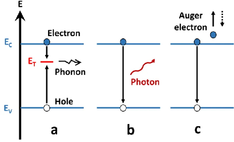
At this point is important to remind the reader that any electron which exists in the conduction band is in a meta-stable state and will eventually stabilize to a lower energy position in the valence band. When this occurs, it will move into an empty valence band state. Consequently, when the electron stabilizes back down into the valence band, it will also effectively remove a hole. The energy difference between the initial and final state of the electron is released in the process. This process is called photo-carrier recombination.[28] In the case of inorganic photovoltaics devices, there are basically three types of photo-carrier recombination: i) radiative, ii) non-radiative, and iii) Auger recombination. As depicted in Figure 2.2a, in the case of non-radiative recombination, this energy is passed on to one or more phonons[29], in the case of radiative recombination, the energy difference between the initial and final state of the electron is emitted in the form of a photon (Figure 2.2b), and in the case of Auger recombination it is given off in the form of kinetic energy to another electron in the conduction band (Figure 2.2c).
Figure 2.2– Recombination mechanisms in inorganic semiconductors: (a) non-radiative, (b) radiative and (c) Auger. In (a) ET denotes de energy level of a defect or impurity in the material also called trap.
Depending on the intrinsic characteristics of the material, photo-carrier recombination trough one of the recombination mechanisms can be more significant than through the others.
For instance, depending on the band gap type, radiative recombination can be more important than non-radiative. We remind the reader that the band gap of a semiconductor material is always either direct or indirect.[26] As depicted in Figure 2.3, this distinction refers to the alignment of the minimal-energy state in the conduction band with respect to the maximal-energy state in the valence band. Indeed, if these two maximal-energy levels are aligned, the band gap is direct, on the contrary, if this energy states are not aligned the band gap is an indirect one. Therefore, radiative photo-carrier recombination is more likely to occur in materials such as gallium arsenide (GaAs) with direct band gaps, while non-radiative Shockley–Read–Hall recombination[30] is usually the predominant recombination type present in Si-based devices favoured by defects and dislocations in the material. Here, is also important to highlight that in highly doped materials, Auger recombination becomes also an important source of energy loss.
Figure 2.3– Photon absorption in direct (left) and indirect (right) bandgap semiconductor. Here the valance band, conduction band, and band gap are denoted as EV, EC and EG respectively.
Actually there are several sources of losses in a solar cell device, some are intrinsic to the material such as the losses due to poor light absorption, and there are other sources of losses that do not depend on the material but rather the device design such as the losses due to the
shadowing effect of the electrodes bus bars over the active material. In fact, to quantify the total solar conversion efficiency η of solar cell devices, the following expression is often used:
𝜂 =𝑉𝑂𝐶𝐼𝑆𝐶𝐹𝐹
𝑃 (2.2) Where 𝑉𝑂𝐶 is the open circuit voltage and can be defined as the electron-hole quasi Fermi level splitting, 𝐼𝑆𝐶 is the short circuit current, this is the current generated when the load resistance is zero, 𝐹𝐹 is the fill-factor which is the ratio of the maximum power generated by the cell divided by 𝑉𝑂𝐶𝐼𝑆𝐶, and 𝑃 is the incident light radiation power. On Earth’s surface, the solar radiation power is approximately 963 Wm−2.[31]
Among different parameters which can be used to describe processes that occur in solar cell devices that impacts their efficiency, carrier lifetime τ is arguably one of the most important ones. This parameter is defined as the time during which an electron excited by light remains in the conduction band before falling back into the valence band. The carrier lifetime must not be confused with the carrier generation lifetime, which is the duration required to convey an electron in the conduction band. Indeed, carrier lifetime plays a central role in the global effectiveness of solar photovoltaic cells since it limits the proportion of photo-generated charges collected on the electrodes.
We have already described the photo-generation process that take place in PV devices, this is, photon absorption and exciton generation. However, photo-generation is only half of the energy conversion process that takes place in PV devices. Actually, in order to take advantage of the energy of the electrons raised to higher energy states, these electrons must be collected. That is actually the main reason why it is desirable to have substantial carrier lifetimes in solar cells, since this allows to maximize the quantity of collected charges.
Nevertheless, for this charge collection to occur, the electrons and holes need to be driven apart to the cathode and the anode respectively which are usually placed at the top and bottom of the solar cell device. For this, a built-in electric field within the cell is usually required. To create this electric field, two semiconductor layers with different doping types are usually “sandwiched” together, creating a p-n junction. A p-n junction consists in one layer of
negatively-doped material, physically connected to another layer of positively-doped material. A p-type semiconductor possesses abundance of positively charged holes while and an n-type semiconductor has an abundance of negatively charged electrons. When n-type and p-type silicon layers contact, excess electrons move from the n-type side to the p-type side. Because of the flow of electrons (and holes), the p-n junction creates the electric field that drive free electrons and holes towards the electrodes as depicted in Figure 2.4.
Connecting conductive leads to both sides of the solar cell will result in the creation of a side-to-side return path within the cell, allowing the process to continue as long as light is provided to the cell. It is this current of electrons traveling from the n-type side to the p-type side through the circuitry and the potential difference between both layers, what define the electrical power that a solar cell can provide. Maximum power is supplied to the electrical load when its impedance matches that of the illuminated PV cell.[31]
Figure 2.4– p-n junction schematic. An exciton is photo-generated, the charges are then separated and guided to the corresponding electrodes. The valence and conduction bands Ev and Ec are identified, as well
as the Fermi level EF, the local vacuum level E0 and the potential Δ created by the junction. The photon’s
energy is defined as ℎ𝑣, which must be higher than the band gap to promote an electron from the valance band to the conduction band.
After near half a century of industrial production, Si-based solar cells are now easily manufactured at large scales, all over the world and especially in China where currently more than half of the world’s photovoltaics are produced.[32] Currently, silicon remains the predominant material used in PV applications, not only because of the mature processing technology, but also for its abundance on earth and well adapted electronic properties. Indeed, silicon has a band gap of 1.12 eV[33] making it suitable for the spectral range[17] of sunlight on earth.
Within silicon based materials, the crystalline quality spans from single crystal to amorphous materials, including materials with different grains size, density and quality of grain boundaries.
In mono-crystalline silicon (c-Si), the wafer material is cut from cylindrical ingots that are typically grown by the Czochralski process.[34] c-Si solar cells display a distinctive pattern of small white diamonds. This material offers the best properties to achieve cell efficiency records. However, the high cost generated by the Czochralski crystal growth is a serious weakness for further increase of the PV cell fabrication.
Unlike mono-crystalline Si-based solar panels, multi-crystalline solar cells, do not require the Czochralski crystal growth process. Instead, for the production of this material, molten silicon is poured into a container and then allowed to cool resulting in silicon ingots with large columnar grains.[31] This means that multi-crystalline solar cells are made from multifaceted silicon crystal, i.e., a crystal that has grown in multiple directions. These materials have the advantage of being less expensive that c-Si however multi-crystalline solar cells are generally 2-3%[31] less efficient than solar cells made of the crystalline material. This reduced efficiency is explained by minority carrier recombination occurring at different defects in the material. Indeed, depending on the crystallization process, the material can have different structural defects, which determine and limit the efficiency of multi-crystalline PV devices. Actually, these defects in the material can act as sinks for photo-excited carriers, negatively impacting the total efficiency. However, in despite of its lower efficiency, multi-crystalline silicon is the most used material at the industrial level[32] because of its reduced manufacturing
cost and the fact that the efficiency gap between c-Si and multi-crystalline solar cells has been reducing over time with the implementation of new design concepts.[19]
On the other side of the spectrum, we find amorphous silicon (a-Si H) which is often used in thin film PV technology applications. Thin films of amorphous silicon are produced using chemical vapour deposition (CVD)[35] of gases containing silane (SiH4).[36] Layers of this material can be deposited onto rigid or flexible substrates depending on the desired application. Actually, the material which is used in solar cells is hydrogenated amorphous silicon, aSi:H, an alloy of silicon and hydrogen, here the hydrogen plays the important role of passivating the dangling bonds that result from the random arrangement of the silicon atoms. Because of its wide band gap (1.7 eV), only a few microns of material are needed to absorb the most energetic (high frequency) incident light.[31]
Actually, it turns out that the microstructure of the deposit can be tuned by diluting the silane gases in hydrogen. In fact, for highly diluted gases, the deposit consists of regions of crystalline silicon immersed in an amorphous matrix. This two-phase material is known as poly-crystalline silicon with grains sizes on the micro/nano-meter range (sometimes also called micro-crystalline silicon). This material shows several useful advantages over a-Si, one being that if grown properly it can have a higher electron mobility, due to the presence of the silicon crystallites.[31] As a-Si, micro-crystalline silicon is often used in silicon thin film PV technologies.
There is a large variety of new emerging silicon PV technologies, the goal of these technologies being to reduce the thickness of the silicon in the panel to minimise materials usage, to increase the light absorption of the material by advanced light trapping techniques, to tune the band gap by the introduction of embedded nanostructures, to prevent photo-carrier recombination and to reduce the energy required in the fabrication process. In short, to improve the economic competitiveness of PV against fossil and non-renewable energy sources. Among these technologies we find black silicon technology,[37] silicon nanocrystals embedded in a dielectric matrix[38] and all-silicon tandem solar cells.[39]
In most of these emerging technologies, where materials are micro/nano-structured, unveiling the photo-transport mechanisms and identifying the sources of losses by carrier recombination is key for their further development. Indeed, investigating the photo-carrier dynamics in nanostructured and heterogeneous energy materials is of crucial importance from both fundamental and technological points of view.
However, emerging PV technologies are not all silicon-based. In fact, there is a wide variety of materials that have been used in the fabrication of photovoltaic devices. As above mentioned, GaAs has a direct energy bandgap as well as other III-V compounds such as indium phosphide (InP) and gallium antimonide (GaSb). These materials possess high optical absorption coefficients and good values of minority carrier lifetimes (in highly pure, single crystal material) rendering them exceptional materials for making high efficiency solar cells.[31] The main disadvantage of photovoltaic devices based on these compounds is the high cost associated to their production with the high quality required for PV applications. In fact, the use of these materials in solar cells has its beginning in space applications where the cost of production did not constitut a drawback against the high-conversion efficiencies together with the high resistance to extra-terrestrial radiation that these materials possess.
Another interesting compound for PV applications is cadmium telluride (CdTe). Indeed, this II-VI compound, which also possess a direct band gap, is commonly used in PV thin film technology applications as well as copper indium gallium (di)selenide (CIGS) which has the advantage of being able to be deposited on flexible substrates, producing highly flexible, lightweight solar panels.
In the 80’s, multi-junction devices (also called tandem devices) were developed. In fact, by adding several junctions, several band gaps can be defined and more energy can be extracted from each incident photon. In other words, the use of multi-junctions allows to minimize energy losses due to electron (and hole) thermalization. As mentioned before, this technology holds the conversion efficiency record with 46%[19], however, theoretical calculations predicts that efficiencies of about 72% could be attained for devices with 32 junctions.[40]
![Figure 3.7–FM-AFM simplified functioning system scheme according to Ref. [21].](https://thumb-eu.123doks.com/thumbv2/123doknet/12691616.355025/83.892.128.770.200.616/figure-fm-afm-simplified-functioning-scheme-according-ref.webp)