HAL Id: hal-01343964
https://hal.archives-ouvertes.fr/hal-01343964
Submitted on 11 Jul 2016
HAL is a multi-disciplinary open access
archive for the deposit and dissemination of
sci-entific research documents, whether they are
pub-lished or not. The documents may come from
teaching and research institutions in France or
abroad, or from public or private research centers.
L’archive ouverte pluridisciplinaire HAL, est
destinée au dépôt et à la diffusion de documents
scientifiques de niveau recherche, publiés ou non,
émanant des établissements d’enseignement et de
recherche français ou étrangers, des laboratoires
publics ou privés.
Analysis and path localization of gate current in
AlGaN/GaN HEMTs using low frequency noise
measurements and Optical Beam Induced Resistance
Change technique
Serge Karboyan, Jean-Guy Tartarin, D Carisetti, B Lambert
To cite this version:
Serge Karboyan, Jean-Guy Tartarin, D Carisetti, B Lambert. Analysis and path localization of gate
current in AlGaN/GaN HEMTs using low frequency noise measurements and Optical Beam Induced
Resistance Change technique. IEEE MTT-S International Microwave Symposium Digest (IMS 2013),
Jun 2013, Seattle, WA, United States. pp.1-4, �10.1109/MWSYM.2013.6697490�. �hal-01343964�
Analysis and Path Localization of Gate Current in AlGaN/GaN
HEMTs Using Low Frequency Noise Measurements and
Optical Beam Induced Resistance Change Technique
S.Karboyan
1,2, J.G. Tartarin
1,2, D. Carisetti
3and B. Lambert
41
LAAS – CNRS, Toulouse, 31031, France
2University of Toulouse, UPS, Toulouse, 31062, France
3Thales Research and Technology, Palaiseau, 91110, France
4United Monolithic Semiconductor, Villebon sur Yvette, 91140, France
Abstract — GaN based transistors’ performance andreliability status are largely sensitive to gate conduction mechanisms and surface charges induced by spontaneous and piezoelectric effects. Understanding leakage current origin and kinetic is the key of knowledge for improving GaN technologies. Therefore, room temperature Low Frequency Noise (LFN) and Optical Beam Induced Resistance Change (OBIRCh) measurements have been investigated on the gate current of AlGaN/GaN High Electron Mobility Transistors (HEMTs). LFN measurements are performed under two configurations: the Schottky diode is measured at open drain, and the transistor is investigated in the saturated region (VDS=8V). On the other hand,
the application of the OBIRCh imaging technique is performed on the Schottky diode versus the same gate voltages than for the LFN. This paper focuses on the behavior of the gate-source region of the Schottky diode and on the source and gate-drain regions of the transistor. From the LFN measurements, it is found that the carriers contributing to IGS are following the same
path between gate and source for both configurations (diode, transistor) under elevated reverse gate-source voltage. As from OBIRCh measurements, a spots spread transmit an increase in the current conduction area on the gate width when VGS
decreases (toward high reverse biases). The results allow correlation between these two techniques.
Index Terms — AlGaN/GaN HEMT, leakage current, LFN, OBIRCh.
I. INTRODUCTION
The benefits induced by the properties of wide band gap transistors result in highly efficient HF devices and circuits. However, using these technologies still poses several problems related to the reliability of devices, and limits the operating time (thus limits the market penetration). It is therefore important to understand the underlying mechanisms causing partial or fatal failures. Many studies have shown that the main sources of degradation are generated within the gate. To emphasize gate defects and current kinetic, cross expertise between different experimental workbenches has been developed. Electrical measurements are carried out, as well as Low Frequency Noise (LFN) measurements and Optical Beam Induced Resistance Change (OBIRCh) characterization on AlGaN/GaN HEMTs, considering two configurations: the analysis of the Schottky diode alone brings fundamental information about the carriers path of the leakage current in
the gate-source region when the drain is open; while studying the transistor under saturated operating mode brings information on the leakage current of the device operating under realistic conditions (amplifiers, oscillators …). LFN measurements (noise spectra versus frequency) are largely used to track defects on the conduction path of the carriers. The evolution of the noise sources with the application of a stress can also give information about the origin of the failure [1-2]. OBIRCh measurements reveal fluctuation of the resistivity in the active irradiated area using a laser beam that induces thermal changes in the device [3-4]. These two techniques are non-destructive for the device, and can be partially correlated.
The paper is organized as follows. In section II, we briefly describe the device structure and the electrical measurements. Sections III and IV report on the results of OBIRCh and LFN measurements respectively. Section V sets the conclusions drawn from the two techniques.
II. DEVICE UNDER TEST AND EXPERIMENTAL CONDITIONS
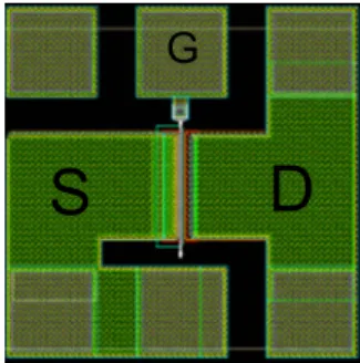
AlGaN/GaN HEMTs (1 finger*100µm*0.5µm, cf. Fig. 1 for a top view) under study are grown on SiC substrate and feature 18% of Al content. The surface is SiN passivated. The Schottky contact is formed by deposition of Ni/Pt/Au.
Fig. 1. Top mask view of the AlGaN/GaN HEMT under study. DC current-voltage measurements are performed using an Agilent 4156C. Fig. 2 shows IG(VGS) characteristics of the
Schottky diode (open drain) and of the transistor when VDS is
biased from 0 to 8V. Diode with shorted drain has also been
D
S
1E-15 1E-13 1E-11 1E-09 1E-07 1E-05 1E-03 -14 -12 -10 -8 -6 -4 -2 IG (A ) VGS(V) VDSbiased 0→ 8 V (step 1V) Schottky diode (open drain) measured and features the same trend as with a slight increase on IG). This study focuses on
IG plots extracted from our measurements (the
the transistor at VDS=8V).
It can be seen that the IG(VGS) trends shift
VGS values when the drain to gate vo
(transistor). The signature of the leakage cur these different biasing conditions. LFN measurements are next performed for reverse
III. GATE CURRENT PATH LOCALIZATION B
MEASUREMENTS
OBIRCh measurements are performed on t than static and LFN measurements. This is stimulation method that heats the metal of th of the metal-semiconductor interface of the conduction. This effect induces an increase of decrease of the resistivity. The wavelength of this study is 1.34 µm. An increase in the curre the presence of red spots in the irradiated ar [2]. These spots highlight the zones where th Fig. 2. DC IG-VGS gate characteristics of the S
solid line) and of the transistor biased from V ΔVDS=1 V (grey to black characteristics).
(a) VGS=-3V (b) VGS=-5V (
Fig. 3. OBIRCh measurements between gate and the transistor: the Schottky diode is biased at VGS
=-D
S
G
#A
#B
#C
0 2 4open drain (with n the two extreme e diode alone and
towards positive oltage increases rrent evolves for and OBIRCh VGS biases.
BY OBIRCH
the same devices s a thermal laser he field plate and gate by thermal f the current by a f the laser used in ent is revealed by rea of the device he current passes.
Results of OBIRCh method on presented in Fig.3.
A spot revealing a very local cu gate width can be observed in Fig. visible at -4V). This spot is spre another one appears closer to the e gate pad in the upper part of the pic and when the gate current homogeneously and #C conduction and #C’ in Fig. 3c).
IV. GATE CURRENT LFNCH
On wafer LFN measurements ar room. A Model 5182 transimpeda The measurements are carried out frequency range of 1 Hz to 100 kHz
The evolution of the gate current spectra versus frequency is given i chottky diode (red
VDS=0 to 8V with (c) VGS=-9V d source regions of -3, -5 and -9V (a) (b) Fig. 4. Gate noise current spectral HEMT (a) of the Schottky diode (open biased in the saturation region at VDS=8
Insets: reverse gate IG-VGS characteristi
SIG LFN measurements are carried out.
#B’
#C’
AlGaN/GaN HEMTs are urrent path at the end of the
3a (#A for VGS=-3V, also
ead at VGS=-5V (#B) and
end of the gate toward the cture (#C). As for VGS=-9V
increases, #B spreads n zone increases (see #B’
HARACTERIZATION
re performed in a shielded ance preamplifier is used. at room temperature in the z.
t Low Frequency Noise SIG
in Fig. 4 for different gate
density of the AlGaN/GaN drain) and (b) of the transistor 8 V.
reverse biases VGS. Fig. 4(a) presents th
performed on the Schottky diode (open drai 4(b) illustrates the measurements on the biased at VDS=8 V). The gate noise level is se
IG varies, even if the SIG spectra evolution i
these two configurations (3 decades for th decade for the transistor over 7V shift on synthesizes the gate current values for the diff under each configuration.
Fig. 5. Gate current noise versus gate current diode (-9V≤VGS≤-2V, black plots) and for the tran
9V≤VGS≤-2V, grey plots).
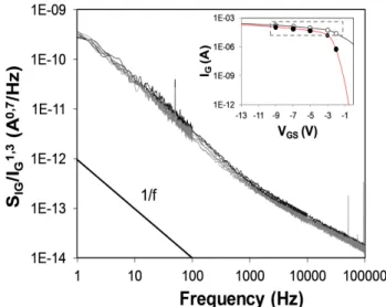
The measurements carried out on the Scho drain) and on the transistor (drain biased at V in Fig. 4(a) and 4(b) exhibit a 1/f trend sup many generation-recombination centers: a r procedure has been developed [6] to accurat noise contributors (the extraction accuracy relative weight of each noise source to the tot the flicker 1/f noise source can be disting many GR centers, as far as its contribution weight to the overall SIG spectra; here, up to 1
needed to fit the SIG spectra, and it is then del
magnitude and the frequency evolution of versus VGS. The raw values are then extract
figure 5. An IG power law of 1.35±0.1 is fou
and for the transistor.
Since it is found that the SIG spectra depe
law of IG1.3, thus the gate current spectral
normalized as SIG/IG1.3 as shown in Fig. 6
signature observed for the diode (-9V≤VGS<
transistor (-9V≤VGS≤-2V) can be imputed to
sources, and thus to the same path for the elec TABLEI
GATE CURRENT VALUES
VGS (V) -2 -3
IG (Schottky diode) (µA) 0.4 12
IG (Transistor) (µA) @ VDS=8 V 17 41
he measurements in), whereas Fig.
transistor (drain ensitive to VGS as s different under he diode, and 1 n VGS). Table 1 fferent VGS biases
t for the Schottky nsistor (VDS=8 V,
-ottky diode (open VDS=8 V) shown
perimposed with robust analytical tely extract each depends on the tal spectra). Then guished from the
n has a valuable 15 GR centers are licate to track the each GR center ted at 100 Hz in und for the diode ends on a power l density can be 6. This identical -3V) and for the o the same noise ctrons within gate
to source (or drain) accesses (same centers above 1 kHz). The leakage c of the same nature for the diode ( and for the transistor (regardless the
For these devices, VGS=-3V stand
two (or more) gate conduction mec SIG of the Schottky diode measured
not fit the IG1.3 power law anymo
engaged leading to a change on the biasing zone, the generation-recom 1/f flicker noise of SIG spectra are
behavior, revealing a change in the the generation-recombination (GR noise of SIG spectra are featuring
revealing a change in the path conduction mode through the gate ( IG-VGS versus analytical models). A
[5], a leakage current model could b contribution of each mechanism.
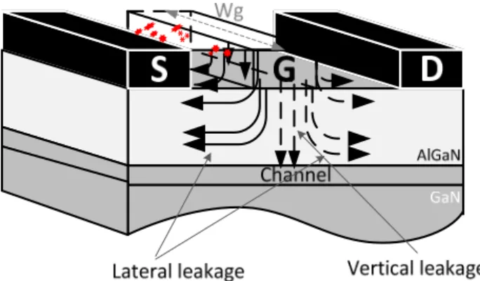
Fig. 7 is a schematic illustration representing where the gate lea location where OBIRCh measure indicated with red spots. Wg is th laser beam irradiates. From our assumed that:
(a) The current path (surface, v mechanisms) occurs in the configurations (between G-S G-S & G-D for the transistor (b) Moreover, whatever the gat proposed VGS ranges), and bo
transistor, the noise spectral d current law (the noise contrib signatures can be partially co Fig. 6. Normalized gate noise curr for the Schottky diode (-9V≤VGS
<-reverse bias, and for the transistor (V plots).
-5 -7 -9 33 51 61 68 86 106
signature, even for the GR current responsible for IG is
(under high reverse biases) e gate bias and at VDS=8V).
ds as a knee value between chanisms: the noise spectra d between -3V ≤VGS<0V do
ore: other mechanisms are e gate current origin. In this mbination (GR) centers and e featuring non monotonic e path of the biasing zone, R) centers and 1/f flicker
non monotonic behavior, of the carriers or in the also confirmed by the fit of According to Zhang and al. be extracted explaining the
of the HEMT under study akage current flows. The
ements are carried out is he gate width wherein the
measurements, it can be vertical, or lateral leakage
same regions for the two S for the diode or between r).
te current value (under the oth for the diode and for the
density evolves with an IG 1.3
butors are the same). These orrelated with the presence rent spectral density SIG⁄IG.
3V, black plots) under high VDS=8 V, -9V≤VGS≤-2V, grey
of very local current paths revealed by OBIRCh technique.
Fig. 7. Illustration of the HEMT AlGaN/GaN structure representing the vertical and lateral gate leakage current paths for the Schottky diode (solid lines) and for the transistor (gate-source diode solid lines and gate-drain diode dashed lines). The red spots illustrate the presence of very local current paths detected by OBIRCh technique.
V. CONCLUSION
This paper presents a synthesis issued from different experimental techniques (Electrical and Low Frequency Noise, OBIRCH) applied to the Schottky diode of an AlGaN/GaN HEMT. Gate conduction mechanisms and gate defects under reverse biasing are investigated in diode configuration and in transistor operating mode. From the investigations, it can be concluded that:
(a) Defects between gate and source are localized by OBIRCh and identified by LFN technique. SIG
spectra feature IG1.3 power law under high reverse
biases, where a common origin of the gate leakage current is found for the diode and for the transistor. Moreover, spots measured by OBIRCh spread on a larger zone of the gate width as the gate to source voltage decreases (high reverse VGS). This is
consistent with the increase of the IG leakage current
when VGS decreases.
(b) Trapping-detrapping centers are also detected with LFN measurements. These GR centers provide distinct trends at the vicinity of VGS=-3V. This is
attributed to a change in the conduction mechanism of the leakage current, also tangible trough the analytical modeling of IG-VGS.
This study introduces a new methodology that can also be used to track gate related defects of AlGaN/GaN HEMT before and after application of stresses. Improvement of technological processes can be reached by the identification and by the reduction of the defects involved in the failure mechanisms.
ACKNOWLEDGEMENT
The authors would like to thank ANR for the funding ReAGaN research program and all the partners of this project for fruitful discussions. They also want to acknowledge the University of Rouen for providing the necessary equipments for OBIRCh measurements.
REFERENCES
[1] H. Rao and G. Bosman “Device reliability study of high gate electric field effects in AlGaN/GaN high electron mobility transistors using low frequency noise spectroscopy,” J. of Applied Physics, vol. 108, September 2010.
[2] J.G. Tartarin, S. Karboyan, F. Olivie, G. Astre and B. Lambert, “I-DLTS, electrical lag and low frequency noise measurements of trapping effects in AlGaN/GaN HEMT for reliability studies,” European Microwave Week Proceedings, 2011. [3] K. Nikawa, S. Inoue, K. Morimoto and S. Sone “Failure analysis
case studies using the IR-OBIRCH (infrared optical beam induced resistance change) method,” Test Symposium,ATS’99 Proceedings. Eighth Asian, 1999.
[4] K. Sanchez, R. Desplats, F. Beaudoin, P. Perdu, S. Dudit, M. Vallet, and D. Lewis, “Dynamic thermal laser stimulation theory and applications,” IEEE Reliability Physics Symposium Proceedings, 2006. 44th Annual, IEEE International.
[5] H. Zhang, E.J. Miller and E.T. Yu “Analysis of leakage current mechanisms in Schottky contacts to GaN and AlGaN/GaN grown by MBE,” J. of Applied Physics, vol. 99, January 2006 [6] J.G. Tartarin, G. Soubercaze-Pun, J.L. Grondin, L. Bary, J.
Mimila-Arroyo and J. Chavallier, “Generation-Recombination defects in AlGaN/GaN HEMT on SiC substrate evidenced by low frequency noise measurements and SIMS characterization,” International Conference on Noise Fluctuations, 2007.