HAL Id: hal-01924812
https://hal.laas.fr/hal-01924812
Submitted on 29 Nov 2018HAL is a multi-disciplinary open access archive for the deposit and dissemination of sci-entific research documents, whether they are pub-lished or not. The documents may come from teaching and research institutions in France or abroad, or from public or private research centers.
L’archive ouverte pluridisciplinaire HAL, est destinée au dépôt et à la diffusion de documents scientifiques de niveau recherche, publiés ou non, émanant des établissements d’enseignement et de recherche français ou étrangers, des laboratoires publics ou privés.
Ring filter synthesis and its BiCMOS 60 GHz
implementation
Pedro Rynkiewicz, Anne-Laure Franc, Fabio Coccetti, Matthias Wietstruck,
Christian Wipf, Selin Tolunay Wipf, Mehmet Kaynak, Gaëtan Prigent
To cite this version:
Pedro Rynkiewicz, Anne-Laure Franc, Fabio Coccetti, Matthias Wietstruck, Christian Wipf, et al.. Ring filter synthesis and its BiCMOS 60 GHz implementation. International Journal of Microwave and Wireless Technologies, Cambridge University Press/European Microwave Association 2018, 10 (03), pp.291 - 300. �10.1017/S1759078718000156�. �hal-01924812�
Ring filter synthesis and its BiCMOS
60-GHz implementation
Pedro Rynkiewicz1, Anne-Laure Franc1, Fabio Coccetti2, Matthias Wietstruck3, Mehmet Kaynak3, Gaëtan Prigent1
1
LAPLACE, University of Toulouse, CNRS, INPT, UPS France.
2
RF Microtech France, Toulouse, France.
3
IHP, Im Technologiepark 25, 15236 Frankfurt (Oder), Germany.
The detailed synthesis of a direct access ring filter topology fully controlled with the following targeted specification (center frequency, low transmission zero frequency and matching level in the passband) is hereby presented. For this topology, the lowest achievable bandwidth is limited by technological constraints. Thereby a solution consisting in adding capacitive loads is proposed. The associated synthesis is also given and discussed. Both syntheses are illustrated with 60 GHz integrated planar filters implemented in the IHP 130 nm BiCMOS technology. Various 3-dB fractional bandwidths from 18% to 8% are targeted, some of them require the implementation of the capacitive loaded solution. The latter allows us to lower the bandwidth limit of the nominal topology as well as to get a high miniaturization, up to 3.4, depending on the capacitance value. Thanks to good measurement results, this implementation highlights the high efficiency, reliability and versatility of the synthesis without the need of tuning simulations or post-simulations.
Corresponding author: A.-L. Franc; email: [email protected];
I.
INTRODUCTION
The congestion of the electromagnetic spectrum and the demand of high data rates devices tend to push the microwave applications to higher frequencies. Recent researches focus on the V-band [40-75 GHz] where various applications are developed like radar, security, medicine, indoor communications and the 5G [1 - 6]. Especially, the 7 GHz unlicensed band around 60 GHz is of great interest for secured broadband communications [7 - 9]. Reaching such high frequencies allows achieving wireless data rates of few Gbits/s [10].
These mass-market applications must be cost-effective, compact and reproducible while ensuring reliable performance. Within this context, BiCMOS appears as one of the most interesting technology [8, 11, 12]. Moreover, it fits with the increasing demand on systems-on-chip that removes the drawbacks of circuits’ interconnections thanks to a full integration [8, 13, 15].
In the telecommunication context, an efficient spectrum discretization is a major challenge; hence bandpass filtering is a key topic. Filters compatible with systems-on-chip are either planar filters or substrate integrated waveguide filters. The latter technology exhibits the better quality factor while being much bulkier [16]. Concerning planar filters, they can be really compact and easy to implement but they usually exhibit a low quality factor (<20) [17 - 24]. To optimize the transmission response while keeping compact size, pseudo-elliptic structures are very interesting. Hence, the presence of transmission zeros in the vicinity of the passband strongly increases the out-of-band rejection while minimizing the filter order and, therefore the insertion loss [20 - 24].
is usually side-coupled and the associated synthesis is presented in [26]. Nevertheless, an easier coupling of the ring filter by direct accesses is presented in [27]. The present work presents the full synthesis of the direct coupling ring filter, for an easy and quick design step. Section II details the ring filter synthesis as well as its technological limitations. An improvement of the synthesis is then proposed to bypass those constraints by the use of capacitive loads along the ring. In section III, several second-order 60 GHz ring filters are designed to highlight the synthesis possibilities. They are implemented using the 130 nm BiCMOS technology provided by IHP microelectronics [28]. Finally, section IV presents a benchmark of 60-GHz integrated filters.
II.
THEORY
A)
Nominal ring filter synthesis
Fig. 1. Nominal ring filter schematic.
The basic ring resonator is a one wavelength-long cell with direct feeds, as depicted in Fig. 1. This topology exhibits a symmetrical quasi-elliptic frequency response, which is controlled by the characteristic impedance values Z1 and Z2, [27].
The proposed synthesis aims at determining the impedance ratio rz = Z2 Z1and the characteristic impedance value Z1, that fit with the requirement in terms of center frequency (fc), low-frequency transmission zero (fTZ) and in-band return loss (y).
With symmetry consideration, the even- and odd-mode analysis is applied. Based on the equivalent schematics presented in Fig. 2, the even-mode impedance, respectively odd-mode impedance, is given by equation (1), respectively (2).
( )
⋅ − ⋅ + + ⋅ = 2 1 2 1 2 1 tan tan 1 1 tan 1 tan tan 1θ
θ
θ
θ
θ
z z z even r r r jY f Y (1)( )
⋅ + ⋅ − + − ⋅ = 2 1 2 1 2 1 cot tan 1 1 cot 1 tan cot 1θ
θ
θ
θ
θ
z z z odd r r r jY f Y (2)where θ1 and θ2 are defined by (3) and (4) with fc the center frequency of the filter.
( )
cf
f
f
=
⋅
2
1π
θ
(3)( )
cf
f
f
=
⋅
4
2π
θ
(4) Z2, λ/4 Z2, λ/4 Z1, λ/4 Z1, λ/4 270° 90° Plane of symmetry IN OUT(a) (b)
Fig. 2. Equivalent schematics for (a) the even mode and (b) the odd mode impedance calculation.
Thereby, one can calculate the transmission parameter S21, with Y0 the normalization admittance (5).
( )
(
) (
)
odd even even odd odd evenY
Y
Y
Y
Y
Y
Y
f
S
+
⋅
+
−
⋅
=
Γ
−
Γ
=
0 0 0 212
(5)1) Control of the low transmission zero frequency
At the low transmission zero frequency fTZ (< fc), S21
( )
fTZ =0. This leads to the resolution of(
TZ)
− even(
TZ)
= 0odd f Y f
Y , with the impedance ratio rz as the unknown variable:
0 tan tan 1 1 tan 1 tan cot tan 1 1 cot 1 tan tan 1 cot 1 2 1 2 1 2 1 2 1 2 2 − = + + + − − + TZ TZ TZ TZ TZ TZ TZ TZ TZ TZ z z z z z z r r r r r r
θ
θ
θ
θ
θ
θ
θ
θ
θ
θ
(6) whereθ
1TZ=
θ
1(
f
TZ)
≤
π
2
andθ
2TZ=
θ
2(
f
TZ)
≤
π
/
4
.After calculation, a quadratic equation depending on 1/rz appears (7). Its resolution finally leads to (8).
Since rz represents an impedance ratio, only the positive solution is considered.
(
1
2
cot
)
0
1
2
tan
cot
2
1
1 2 2 1 2=
+
−
⋅
−
TZ TZ TZ z zr
r
θ
θ
θ
(7) 1 2 2 1 2 21 cot2 2 tan cot 2
cot − + + + = TZ TZ TZ TZ z r
θ
θ
θ
θ
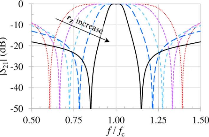
(8)Figure 3 illustrates the electric response of the filter when the ratio rz varies. Only the transmission zero
frequencies are affected by an rz change.
Fig. 3. Dependence of the electric response with rz=Z2/Z1. (rz varies from 0.5 to 0.9, the return loss is set to 20 dB.). 2) Passband matching control
At the center frequency, the even- and odd-mode admittance expressions are as follow:
Z2 , λ /8 Z1, λ/4 Yeven Z2 , λ /8 Z1, λ/4 Yodd Z2 , λ /8 Z2 , λ /8 -50 -40 -30 -20 -10 0 0.50 0.75 1.00 1.25 1.50 |S2 1 | (dB ) f / fc
( )
f jY(
r r)
jY BYeven c = − 1⋅ z −1 z = − 1⋅ , (9)
( )
f jY(
r r)
jY BYodd c = 1⋅ z −1 z = 1 ⋅ , (10)
with B defined as B=rz −1 rz.
Finally, the filter transmission at the center frequency can be written as:
( )
2 2 1 2 0 1 0 21 2 B Y Y B Y jY f S c + = . (11)By imposing y the return loss, the passband ripple x is such as: 10 /
10
1 y
x= − − . (12)
By equaling the modulus of (11) and (12), a quadratic equation appears with Y1 as unknown variable.
Its resolution leads to two solutions for the value of Z1 (13). The one with the minus sign corresponds to
an over-coupled filter response (Fig. 4) therefore the solution with the plus sign is preferred. 1 2 0 1
1
1
−
±
−
⋅
⋅
=
x
B
x
Y
Z
(13)Fig. 4. Electric response with the two Z1 solutions of equation (13).
(The low transmission zero frequency equals 0.725·fc, thus, the impedance ratio rz is 0.7.)
Figure 5 illustrates the control of the in-band return loss with Z1 for a given low transmission zero
frequency (0.725·fc), setting impedance ratio rz to 0.7. The bandwidth (that is only controlled by the
transmission zero frequency, i.e. rz) is the same for all the simulations presented in Fig. 5.
Fig. 5. Dependence of the electric response with Z1 value. (The impedance ratio rz is set to 0.7.) 3) Limitation
As the impedance ratio directly implies the low transmission zero frequency, it also sets the bandwidth. -40 -30 -20 -10 0 0.50 0.75 1.00 1.25 1.50 |S -p ar am et er s| ( d B ) f / fc - sign + sign -0.2 -0.1 0.0 0.9 1.0 1.1 -50 -40 -30 -20 -10 0 0.50 0.75 1.00 1.25 1.50 |S -pa ra m et er s| ( dB ) f / fc Z1 =26.1 Ω Z1= 32.7 Ω Z1= 35Ω Z1= 35.8 Ω
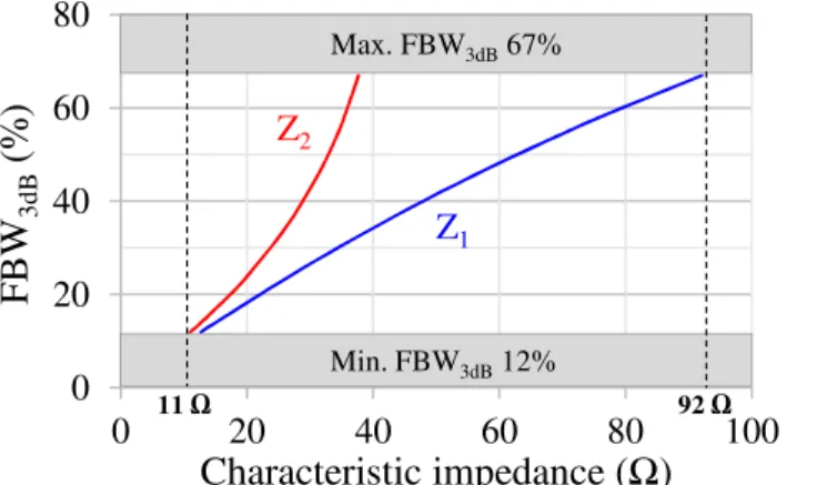
Thus, for a given technology, the extent of the achievable bandwidth relies only on the characteristic impedance range. For instance, Fig. 6 depicts the achievable bandwidth as a function of the impedance values Z1 and Z2. If an impedance range from 11 Ω to 92 Ω is considered, the achievable 3-dB
fractional bandwidth (FBW3dB) varies from 12% to 67%. Thereby, this topology is dedicated to filters
with medium to relative wide bandwidth. (Note that the considered impedance range relies on the BiCMOS 130nm microstrip technology that will be presented later in this paper.)
Fig. 6. Achievable 3-dB fractional bandwidth around 60 GHz as a function of the characteristic impedances Z1 and Z2.
B)
Capacitive-loaded ring filter synthesis
1) Bandwidth reduction
In order to reduce the achievable bandwidth, an evolution of the topology is presented using capacitive loading. Each side of the ring is loaded at its center by a capacitor as shown in Fig. 7.
Fig. 7. Capacitive-loaded ring filter schematic.
Considering the equivalent networks depicted in Fig. 8, the ABCD matrix of each circuit can be easily determined, Zi_C being the characteristic impedance of the loaded transmission line and θi_C its electrical
length. Comparing the ABCD matrix, equations (14) and (15) appear with
ω
c =2π
fc.(
)
sin(
2)
0 2 2 cosθ
i_c −Ciω
cZi_cθ
i_c = (14)(
)
[
(
i c)
]
i C i i c i c i Z Z C Z − − _ = 2 _ _ _ 1 cos 2 2 2 sinθ
θ
(15) 0 20 40 60 80 0 20 40 60 80 100 F B W 3 d B (% ) Characteristic impedance (Ω) Z1 Max. FBW3dB67% Min. FBW3dB12% 11 Ω 92 Ω Z2 IN C1 Z1_C , θ1_C Z1_C , θ1_C C2 Z2_C , θ2_C Z1_C, θ1_C Z1_C , θ1_C Z2_C, θ2_C Z2_C , θ2_C Z2_C , θ2_C C1 C2 OUT 270° 90°Fig. 8. (a) A capacitive-loaded transmission line and (b) its equivalent conventional transmission line model.
Equation (14) directly gives the required electrical lengths θi_C (16).
= c i C i C i C Z ω θ _ _ 2 arctan 2 1 (16)
The resolution of (15), knowing expression (16), leads to:
c i i i C i C Z Z Z
ω
− = 1 _ . (17)Figures 9 and 10 display the bandwidth and electrical length variations versus normalized capacitor value
(
CN =Z0Cωc)
. The nominal circuit corresponds to C equal to zero; then the capacitive loading is applied with four identical capacitors (C1=C2=C) while forcing the impedance values to thosedetermined by the nominal synthesis (Zi_C=Zi). As shown in Fig. 9, the higher the capacitor value, the
lower the fractional bandwidth. Hence, for a given technology, the capacitive-loaded topology allows reaching lower bandwidths than the nominal one. Moreover, the electrical lengths decrease (see Fig. 10), thus strongly minimizing the size of the filter.
Fig. 9. 3-dB fractional bandwidth as a function of the capacitive loading for C1=C2=C and given values of Z1_C and Z2_C corresponding to the nominal synthesis applied with fTZ=0.725·fc and y=20 dB
(i.e. Z1_C=Z1=32.7 Ω and Z2_C=Z2=23 Ω). 0 5 10 15 20 25 30 0 1 2 3 4 5 F B W3 d B (% ) CN 0 10 20 30 40 50 0 1 2 3 4 5 θ (° ) CN θ2 θ1 (a) (b) Ci
Fig. 10. Electrical lengths as a function of the capacitive loading for C1=C2=C and given values of Z1_C and Z2_C corresponding to the nominal synthesis applied with fTZ=0.725·fc and y=20 dB. 2) Design versatility
In terms of implementation, this capacitive-loaded topology offers a high flexibility since the design requires four values {C1, Z1_C} and {C2, Z2_C}. With these degrees-of-freedom, several filter topologies
can be designed to meet the specifications with respect to the technological constraints (available capacitances or characteristic impedances) and the targeted specifications (surface miniaturization or minimization of the insertion loss).
III. 60 GHz FILTERS DESIGN
In this section, six second-order filters are presented to validate the previous synthesis with and without the capacitive loads.
A)
Technology
All the realized circuits have been implemented in the IHP’s 130nm SiGe BiCMOS technology presented in Fig. 11. The stack is made of seven aluminum layers including two thick top metals all of them drown in the SiO2. The via holes between layers are made of tungsten and a Si3N4 passivation
layer covers the whole die. The process also includes MIM capacitors.
Fig. 11. IHP’s 130nm SiGe BiCMOS Back-End-of-Line.
Thin film microstrip transmission lines are used in this work. The lowest layer, Metal 1, is used as ground plane and the highest and thickest one, Top Metal 2 (3 µm-thick), is used as signal line. This allows both decreasing the conductive losses and getting a large impedance range.
Figure 12 shows the 60-GHz simulated impedance and attenuation constant values versus the transmission-line width. The characteristic impedance range is [11 Ω, 92 Ω]. The highest value is set by the Top Metal 2 width limit (2 µm) given by the design rules. The lowest reachable impedance is 11 Ω for a 140 µm signal width. Larger microstrips might be considered but, for realistic applications, a reasonable shape factor has to be kept between the width and the quarter-wavelength (660 µm at 60 GHz) so that the transitions remain negligible. The simulated attenuation constant hardly depends on the value of the characteristic impedance and remains lower than 0.6 dB/mm at 60 GHz.
Fig. 12. 60-GHz simulated characteristic impedance and attenuation constant for microstrip transmission lines implemented in IHP 130nm BiCMOS.
B)
Nominal ring filters
As seen in the theoretical part (Section II), the lowest impedance sets the narrowest bandwidth. Hence, theoretically, considering the lowest 11 Ω impedance, the FBW3dB is limited to 12%. In this part, two
60 GHz nominal ring filters (Fig. 1) are proposed with 18%- and 12%-FBW3dB. They are composed of
quarter-wavelength transmission lines whose characteristic impedances given by the synthesis are summarized in Table 1. Both ring filters are simulated and slightly optimized using the finite-element-method-based software Ansys HFSSTM.
Table 1. Characteristic impedances and associated microstrip widths of the λ/4 transmission lines composing the nominal ring filters.
TLines 1 TLines 2
Z1 W Z2 W
Nominal 18% 23.6 Ω 50 µm 18.3 Ω 75 µm Nominal 12% 13.4 Ω 107 µm 11.6 Ω 126 µm
The circuits’ photographs are shown in Fig. 13. Excluding the access lines and RF-pads, the filter footprint is 0.51 mm² for the 18%-FBW3dB resonator while it is 0.61 mm
2
for the 12%-FBW3dB
resonator. (The metal squares in the center of the ring are dummies required to pass the technology density rules.)
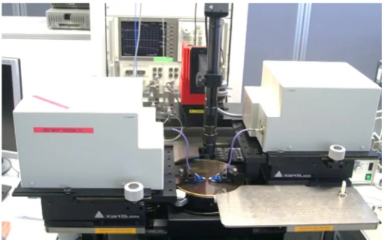
Fig. 13. Photographs of the nominal ring filters: (a) 18% FBW3dB filter and (b) 12% FBW3dB filter. The measurements of these filters were carried out up to 110 GHz with the setup shown in Fig. 14. All measurements, obtained after deembedding using on-wafer TRL calibration kit [29], are in a very good agreement with the simulation results, see Fig. 15 and 16.
0 0.2 0.4 0.6 0.8 1 0 20 40 60 80 100 0 20 40 60 80 100 120 140 A tt enua ti on c ons ta nt (dB /m m ) Im pe da nc e (Ω ) Width (µm) (a) (b)
Fig. 14. On-wafer measurement setup.
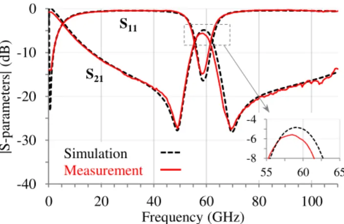
Fig. 15 displays the 18% FBW3dB nominal ring results. The simulation predicts a 3.4 dB insertion loss
while the measurements exhibit 4.3 dB for a 20.1% FBW3dB which is slightly enlarged compared to the
expected 18%. The measured center frequency is shifted by 1 GHz to higher frequencies and the matching level is very good (>18 dB).
In Fig. 16, the measurement fits very well with the simulations on the whole frequency band: The measured FBW3dB is 12.5% compared to the 12% expected by the simulation and the measured
insertion loss is 5.8 dB compared to the simulated 5.7 dB.
Fig. 15. Simulated and measured S-parameters of the 18% FBW3dB nominal ring filter.
Fig. 16. Simulated and measured S-parameters of the 12% FBW3dB nominal ring filter.
The very good agreement between the simulation and the measurement results proves the high reliability of the nominal synthesis and the high level of confidence and accuracy of the design models. Actually, as no modification on the synthesis values has been done (except negligible changes to take the corners electromagnetic effects into account), it is very convenient for designers to use and target
-40 -30 -20 -10 0 0 20 40 60 80 100 |S -p ar am et er s| ( d B ) Frequency (GHz) Simulation Measurement S21 S11 -7 -5 -3 55 60 65 -40 -30 -20 -10 0 0 20 40 60 80 100 |S -p ar am et er s| ( d B ) Frequency (GHz) Simulation Measurement S21 S11 -8 -6 -4 55 60 65
filters with given technical specifications.
The main limitation of this nominal synthesis is the very low required impedances for narrow-band filters (see Fig. 12). For instance, the filter with 12% FBW3dB of Fig. 13 (b) requires microstrips as large
as 126 µm, i.e. λ/20, which is bulky and not convenient for the design. So, next part will focus on the capacitive-loaded ring filter synthesis that allows the designer to easily reach narrower bandwidths.
C)
Capacitive-loaded ring filters
Using the capacitive-loaded ring filter synthesis presented in part II.B), four filters were designed at 60 GHz (schematic Fig. 7 with the same capacitors, i.e. C1=C2=C). For comparison purposes with the
nominal one, two filters were designed to get a 12% FBW3dB with two different capacitor values. Then,
to push the limit of narrow bandwidth, two 8% FBW3dB filters were designed. They also differ in terms
of the used capacitances. All capacitances obtained with the synthesis were implemented with Metal-Insulator-Metal capacitors available in the process.
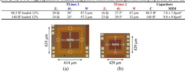
1) 12% capacitive-loaded ring filter
Two 12% FBW3dB filters were designed with either capacitances of 88.5 fF or 140 fF. All the electrical properties from the synthesis as well as the physical dimensions are summarized in Table 2. The two ring filters are shown in Fig. 17. The one using 88.5 fF capacitors has a surface area of 0.39 mm2 and the one with 140 fF capacitors requires both thinner and shorter transmission lines and only requests 0.18 mm2.
Table 2. 12% FBW3dB capacitive-loaded ring filters electrical and geometrical properties at 60 GHz.
TLines 1 TLines 2 Capacitors
Z1 ϴ1 W Z2 ϴ2 W C MIM
88.5 fF loaded 12% 20 Ω 36° 87.5 µm 16 Ω 37.5° 67 µm 88.5 fF 7.8 x 7.8µm² 140.fF loaded 12% 34 Ω 24° 57.2 µm 23 Ω 29.5° 32 µm 140 fF 9.8 x 9.8µm²
Fig. 17. Photographs of the capacitive-loaded 12% FBW3dB ring filters with (a) 88.5 fF and (b) 140 fF capacitors.
The measurement and the simulation results of these 12% FBW3dB capacitive-loaded ring filters are
shown in Fig. 18 and 19. In both cases, the measured center frequency, return loss and FBW3dB agree
very well with the simulation results. The measured insertion loss is 5.6 dB, whereas the nominal filter exhibits 5.8 dB insertion loss for identical bandwidth.
With almost similar electrical performance, the 12% FBW3dB capacitive-loaded topology is much more
compact than the nominal one. Moreover, the higher the capacitance is, the stronger the miniaturization is (up to a factor 3.4 with 140 fF capacitors).
Those results also highlight how efficient the proposed synthesis is. Actually, this double synthesis (with and without capacitors) allows a very high flexibility for the designer. Hence, for a given specification, the designer can choose either to use a nominal topology without capacitors (e.g. if not available in the technology) or to implement capacitive-loaded ring to target a specific miniaturization in adjusting the capacitor values.
Fig. 18. Simulated and measured S-parameters of the 12% FBW3dB ring filter loaded with 88.5 fF capacitors.
Fig. 19. Simulated and measured S-parameters of the 12% FBW3dB ring filter loaded with 140 fF capacitors.
2) Narrow-band capacitive-loaded ring filters
The miniaturization purpose is a great advantage of the capacitive-loaded topology. Nevertheless, another strong benefit is to allow reaching narrow bandwidths that cannot be achieved with the nominal structure.
As previously mentioned, according to the technological limitations in the 130 nm BiCMOS process, the 3dB-bandwitdth of the nominal ring filter topology has a lower limit of 12%. To bypass this limitation, 8% FBW3dB ring filters at 60 GHz are realized with the capacitive-loads and associated
synthesis. Two filters are implemented with two capacitance values to compare the electrical performance and validate the synthesis in different cases.
All the electrical and dimension characteristics are given in Table 3. The capacitive-loaded ring filter with an 88.5 fF capacitance requires a 0.47 mm2 surface area while the circuit using a 160 fF capacitance has an on-chip area of 0.38 mm2 (Fig. 20). Once again, the measurements and simulations (Fig. 21 and 22) are in a very good agreement. For the 88.5 fF loaded ring, the insertion loss reaches 7.7 dB and the return loss 14 dB whereas the 160 fF loaded ring filter exhibits an 8.7 dB insertion loss and an 11 dB return loss.
Table 3. 8% FBW3dB capacitive-loaded ring filters electrical and geometrical properties at 60 GHz.
TLines 1 TLines 2 Capacitors
Z1 ϴ1 W Z2 ϴ2 W C MIM 88.5 fF loaded 8% 13.4 Ω 38.5° 107.5 µm 11.6 Ω 39.5° 126 µm 88.5 fF 7.8 x 7.8µm² 160 fF loaded 8% 14.1 Ω 33.5° 102.5 µm 12 Ω 35° 121.5 µm 160 fF 10.3 x 10.3µm² -40 -30 -20 -10 0 0 20 40 60 80 100 |S -p ar am et er s| ( d B ) Frequency (GHz) Simulation Measurement S21 S11 -8 -6 -4 55 60 65 -40 -30 -20 -10 0 0 20 40 60 80 100 |S -p ar am et er s| ( d B ) Frequency (GHz) Simulation Measurement S21 S11 -8 -6 -4 55 60 65
Fig. 20. Photographs of the capacitive-loaded 8% FBW3dB ring filters with (a) 88.5 fF and (b) 160 fF capacitors.
Fig. 21. Simulated and measured S-parameters of the 8% FBW3dB ring filter loaded with 88.5 fF capacitors.
Fig. 22. Simulated and measured S-parameters of the 8% FBW3dB ring filter loaded with 160 fF capacitors.
This section is a complete application of the nominal and capacitive-loaded ring filter synthesis. The validation is carried out on moderate-band 60-GHz filters with 3-dB fractional bandwidth of 18%, 12% and 8%. It highlights the high flexibility of the topology depending on both the expected size reduction and the technology (e.g. capacitors available or not, which capacitor values).
It is also worth mentioning that the direct synthesis application gives directly good electromagnetic performance (no tuning and no post-simulation are required). Moreover, it also confirms the very good reliability of the BiCMOS process.
-40 -30 -20 -10 0 0 20 40 60 80 100 |S -p ar am et er s| ( d B ) Frequency (GHz) Simulation Measurement S21 S11 -11 -9 -7 55 60 65 -40 -30 -20 -10 0 0 20 40 60 80 100 |S -p ar am et er s| ( d B ) Frequency (GHz) Simulation Measurement S21 S11 -11 -9 -7 55 60 65 (a) (b)
IV.
BENCHMARK
In this section, a benchmark is performed between several 60-GHz bandpass filters implemented in various CMOS technologies, see Table 4. Medium bandwidths are considered and a special attention is given to determine if those filters are fully dimensioned based on a published synthesis. In addition, they are compared in terms of required surface area and electrical performance. To take both the insertion loss and the bandwidth into account, a quality factor calculation is made with the approximation (18), introduced by Cohn in [30]. Since the gk are the coefficients of the n
th
order Butterworth polynomial, this approximation is accurate for filters showing a Butterworth response. Hence to fairly compare the filters presented in Table 4, the quality factor is calculated only for pseudo-elliptic second-order filters, i.e. having a good rejection on both sides of the passband. (Those do not present a Butterworth electric response but no accurate approximation exists in this particular case.) For second order filters, the approximation of (18) becomes (19).
dB n k k u
FBW
IL
g
Q
3 1343
.
4
×
⋅
=
= (18) dB uIL
FBW
Q
nd 3 2 _8
.
14
×
=
(19)Table 4. Medium band CMOS bandpass filters around 60 GHz.
Technology Available synthesis Frequency FBW3dB IL QU_2nd* Surface area Ref.
CMOS QMSIW No 60.5 GHz 11.6 % 2.5 dB N.A. 1.7 mm² [16] 180 nm CMOS Yes Coupled lines [31] 60 GHz 10 % 9.3 dB N.A. 0.14 mm² [17] No 60 GHz 13.3 % 3.1 dB N.A. 0.032 mm² [19] 65 nm CMOS No 53.4 GHz 16.5 % 5.5 dB 16.3 0.09 mm² [20] 90 nm CMOS No 59 GHz 24.6 % 4.2 dB 14.4 0.12 mm² [21] 130 nm CMOS Yes Dual Behavior
Resonator [32] 60 GHz 17 % 4.1 dB 21.2 0.29 mm² [22] 180 nm CMOS No 60 GHz 30 % 3.5 dB 14.1 0.034 mm² [23] No 60 GHz 26 % 4 dB 14.2 0.185 mm² [24] Yes Nominal Ring Filter 60GHz 20.1 % 4.3 dB 17.1 0.51 mm2 This Work Nominal 18% 12.5 % 5.8 dB 20.4 0.61 mm2 Nominal 12% Capacitive- loaded ring filter 11.8 % 5.6 dB 22.4 0.39 mm2 88.5 fF Loaded 12% 11.3 % 5.6 dB 23.4 0.18 mm2 140 fF Loaded 12% 9.3 % 7.7 dB 20.7 0.47 mm2 88.5 fF Loaded 8% 8 % 8.7 dB 21.3 0.38 mm2 160 fF Loaded 8% * QU_2nd is calculated only for second-order pseudo-elliptic responses.
The quarter-mode substrate integrated waveguide filter in [16] shows the lowest loss but also the largest footprint reported in Table 4. The lumped-element-based bandpass filter in [19] displays very interesting electrical performance and is really compact but, without transmission zeros close to the passband, its out-of-band rejection is not sharp enough and reaches only 10 dB at 90 GHz.
Among the quasi-elliptic response, the solutions presented in [20, 21, 23, 24] exhibit similar electric performance since their quality factors are between 14.1 and 16.3. They differ in surface area, the filter of [23] being the most compact with only a 0.034 mm2 footprint. Even if the solution of [21] is based on a thorough analysis reported in [33], none of those filters is based on a synthesis, i.e. the electrical properties are not directly given by the targeted technical specifications.
Finally, three solutions designed with a full synthesis remain: [17] is based on coupled lines design, [22] uses dual behavior resonators and the filters of the present paper. The 60-GHz conventional coupled lines filter of [17] is more compact than the present work but the associated insertion loss are the highest referenced in this state-of-the-art and it is not pseudo-elliptic so difficult to truly compared with others. In [22], low losses are measured thanks to both a compact slow-wave structure and copper metal layers. This leads to a good 21.2 quality factor. The present work, implemented with aluminum metal layers, exhibit quality factors ranging from 17.1 to 23.4. As the highest value is obtained for the loaded solution with high capacitances, it also presents the advantage to be quite compact.
V.
CONCLUSION
The synthesis for direct access ring filter is detailed. The characteristic impedances of the quarter-wavelength transmission lines are fully determined with the targeted electrical response defined with the center frequency, the low-frequency transmission zero and the return loss level. To decrease the achievable bandwidth, capacitors are added in the filter topology and the synthesis is therefore updated. This evolution leads to a miniaturization and to an important versatility of the synthesis as various degrees-of-freedom can be adjusted by the designer.
Finally, the two syntheses are implemented at millimeter-wave in a 130-nm BiCMOS technology. Two nominal ring filters are measured at 60 GHz: the first exhibits an 18% FBW3dB for a 4.3 dB insertion
loss and the second has 5.8 dB of insertion loss for a 12% FBW3dB. To highlight the flexibility of the
capacitive-loaded filter synthesis, two 12% FBW3dB filters with different capacitances are characterized.
They exhibit very similar electrical responses as the nominal topology but are much more compact (up to a factor 3.4). Finally, to push the limit of low bandwidth, two capacitively loaded filters with different capacitor values are implemented to reach an 8% FBW3dB.
ACKNOWLEDGEMENT
The authors would like to thank Christian Wipf and Barbaros Cetindogan, IHP (Germany), for their assistance and the on-wafer measurements.
REFERENCES
[1] Ulaganathan, R. V.; Eibert, T. F.; Baheti, A.; Jungmaier, R. W.; Trotta, S.; Eisenberg, G.: Beamforming with
multi-channel V-Band system-on-chip radar platform for gesture sensing, 13th European Radar Conference,
London, UK, 2016.
[2] Kumar, B.; Upadhyay, R.; Singh, D.: Critical analysis of signal processing techniques for concealed weapon
identification with MMW (60 GHz) imaging radar system, 10th International Conference on Industrial and
Information Systems, Peradeniya, Sri Lanka, 2015.
[3] Gao, Y.; Zoughi, R.: Millimeter Wave Reflectometry and Imaging for Noninvasive Diagnosis of Skin Burn Injuries, Transactions on Instrumentation and Measurement, 66 (1) (2017), 77-84.
[4] Collonge, S.; Zaharia, G.; El Zein, G.: Wideband and Dynamic Characterization of the 60 GHz Indoor Radio Propagation Future Home WLAN Architectures, Annals of Telecommunications, 58 (3-4) (2003), 417-447. [5] Jia, H.; Chi, B.; Kuang, L.; Yu, X.; Chen, L.; Zhu, W.; Wei, M.; Song, Z.; Wang, Z. : Research on CMOS mm-wave circuits and systems for wireless communications, China Communications, 12 (5) (2015), 1-13.
[6] Scott-Hayward, S.; Garcia-Palacios, E.; Multimedia resource allocation in mmwave 5G networks, IEEE Communications Magazine, 53 (1) (2015), 240-247.
[7] Rappaport, T. S.; Murdock, J. N.; Gutierrez, F.: State of the Art in 60-GHz Integrated Circuits and Systems for Wireless Communications, Proc. of the IEEE, 99 (8) (2011), 1390-1436.
[8] Urushihara, T.; Takahashi, H.; Kobayashi, M.; Motozuka, H.; Irie, M.; Shirakata, N.; Takinami, K.: 60GHz wireless technologies for WiGig/IEEE 802.11ad multi-gigabit systems, Asia-Pacific Microwave Conference, Sendai, Japan, 2014.
[9] Smulders, P.; Yang, H.; Akkermans, I.; On the Design of Low-Cost 60-GHz Radios for Multigigabit-per-Second Transmission over Short Distances [Topics in Radio Communications], IEEE Communications Magazine,
45 (12) (2007), 44-51.
[10] Yong, S. K.; Chong, C.-C.: An overview of multigigabit wireless through millimeter wave technology: Potentials and technical challenges, EURASIP J. on Wireless Communications and Networking, 2007 (1) (2007), 1–10.
[11] Floyd, B.; Valdes Garcia, A.; Reynolds, S. ; Natarajan, A. ; Liu, D. ; Gaucher, B. ; Nakano, D. ; Katazama, Y. : Silicon millimeter-wave radios for 60 GHz and beyond, International Symposium on VLSI Technology, System and Application, Hsinchu, Taiwan, 2010.
[12] Tillack, B.: SiGe BiCMOS platform - baseline technology for More Than Moore process module
integration, 14th IEEE International Symposium on Design and Diagnostics of Electronic Circuits and Systems,
[13] Song, Y.; et al.: A Hybrid Integrated High-Gain Antenna With an On-Chip Radiator Backed by Off-Chip Ground for System-on-Chip Applications, IEEE Trans. on Components, Packaging and Manufacturing Technology, 7 (1) (2017), 114-122.
[14] Sarkar, S.; Laskar, J.: A Single-Chip 25pJ/bit Multi-Gigabit 60GHz Receiver Module, International Microwave Symposium, Honolulu, USA, 2007.
[15] Liu, C. C.; Rojas, R. G.: V-Band Integrated on-Chip Antenna Implemented With a Partially Reflective Surface in Standard 0.13 µm BiCMOS Technology, IEEE Trans. on Antennas and Propagation, 64 (12) (2016), 5102-5109. [16] Senior, D. E.; Rahimi, A.; Yoon, Y.-K.: A Surface Micromachined Broadband Millimeter-Wave Filter using Quarter-Mode Substrate Integrated Waveguide Loaded with Complementary Split Ring Resonator, International Microwave Symposium Digest, Tampa bay, USA, 2014.
[17] Nan, L.; Mouthaan, K.; Xiong, Y. Z.; Shi, J.; Rustagi, S. C.; Ooi, B. L.: Design of 60- and 77-GHz Narrow-Bandpass Filters in CMOS Technology, IEEE Trans. on Circuits and Systems II: Express Briefs, 55 (8) (2008), 738-742.
[18] Vanukuru, V. N. R.; Velidi, V. K.: Millimeter-wave ultra-wideband bandpass filter with quarter-wavelength short-stubs and port extensions using 0.18-μm CMOS process, International Conference on Electron Devices and Solid-State Circuits, Singapore, 2015.
[19] Vanukuru, V. N. R.: Millimeter-wave bandpass filter using high-Q conical inductors and MOM capacitors, Radio Frequency Integrated Circuits Symposium, San Francisco, USA, 2016.
[20] Yang, B.; Skafidas, E.; Evans, R. J.: Slow-wave slot microstrip transmission line and bandpass filter for compact millimetre-wave integrated circuits on bulk complementary metal oxide semiconductor, IET Microwaves, Antennas & Propagation, 6 (14) (2012), 1548-1555.
[21] Lu, H.-C.; Yeh C.-S.; Wei, S.-A: Miniaturised 60 GHz rectangular ring bandpass filter in 90nm CMOS technology, Electronics Letters, 47 (7) (2011), 448-450.
[22] Franc, A.-L.; Pistono, E.; Gloria, D.; Ferrari, P.: High-Performance Shielded Coplanar Waveguides for the design of CMOS 60-GHz bandpass filters, IEEE Trans. on Electron Devices, 59 (5) (2012), 1219-1225.
[23] Chen, Y. C.; Yeh, L. K.; Chuang, H. R.: Design of ultra-compact 60-GHz millimeter-wave CMOS on-chip bandpass filter with two controllable transmission zeros, Asia-Pacific Microwave Conference, Sendai, Japan, 2014. [24] Ma, K.; Mou, S.; Yeo, K. S.: Miniaturized 60-GHz On-Chip Multimode Quasi-Elliptical Bandpass Filter, IEEE Electron Device Letters, 34 (8) (2013), 945-947.
[25] Wolff, I.: Microstrip bandpass filter using degenerate modes of a microstrip ring resonator, Electronics Letters,
8 (12) (1972), 302-303.
[26] Mohd Salleh, M. K.; Prigent, G.; Pigaglio, O.; Crampagne, R.: Quarter-Wavelength Side-Coupled Ring Resonator for Bandpass Filters, IEEE Trans. on Microwave Theory and Techniques, 56 (1) (2008), 156-162.
[27] Franc, A.-L.; Prigent, G.: Compact capacitive loaded ring filter with simplified feeding lines, 44th European
Microwave Conference, Rome, Italy, 2014.
[28] Tolunay Wipf, S.; Göritz, A.; Wietstruck, M.; Tillack, B.; Mai, A.; Kaynak, M., Thin film wafer level
encapsulated RF-MEMS switch for D-band applications, 46th Europ. Microw. Conf., London, UK, 2016.
[29] Engen, G. F.; Hoer, C. A.: Thru-Reflect-Line: An Improved Technique for Calibrating the Dual Six-Port Automatic Network Analyzer, IEEE Trans. on Microwave Theory and Techniques, 27 (12) (1979), 987-993. [30] Cohn, S. B.: “Dissipation Loss in Multiple-Coupled-Resonator Filters,” Proc. of the IRE, 47 (8) (1959), 1342-1348.
[31] Matthaei, G. L.; Young, L.; Jones, E. M. T.: Microwave Filters, Impedance-Matching Networks, and Coupling Structures, Norwood, MA: Artech House, 1980.
[32] Quendo, C.; Rius, E.; Person, C.: Narrow bandpass filters using dual-behavior resonators, IEEE Trans. on Microwave Theory and Techniques, 51 (3) (2003), 734-743.
[33] Lei, M.-F.; Wang, H.: An analysis of miniaturized dual-mode bandpass filter structure using shunt-capacitance perturbation, IEEE Trans. on Microwave Theory and Techniques, 53 (3) (2005), 861-867.
List of figures and tables
Fig. 1. Nominal ring filter schematic.Fig. 3. Dependence of the electric response with rz=Z2/Z1. (rz varies from 0.5 to 0.9, the return loss is set
to 20 dB.).
Fig. 4. Electric response with the two Z1 solutions of equation (13). (The low transmission zero
frequency equals 0.725·fc, thus, the impedance ratio rz is 0.7.)
Fig. 5. Dependence of the electric response with Z1 value. (The impedance ratio rz is set to 0.7.)
Fig. 6. Achievable 3-dB fractional bandwidth around 60 GHz as a function of the characteristic impedances Z1 and Z2.
Fig. 7. Capacitive-loaded ring filter schematic.
Fig. 8. (a) A capacitive-loaded transmission line and (b) its equivalent conventional transmission line model.
Fig. 9. 3-dB fractional bandwidth as a function of the capacitive loading for C1=C2=C and given values
of Z1_C and Z2_C corresponding to the nominal synthesis applied with fTZ=0.725·fc and y=20 dB (i.e.
Z1_C=Z1=32.7 Ω and Z2_C=Z2=23 Ω).
Fig. 10. Electrical lengths as a function of the capacitive loading for C1=C2=C
and given values of Z1_C and Z2_C corresponding to the nominal synthesis
applied with fTZ=0.725·fc and y=20 dB.
Fig. 11. IHP’s 130nm SiGe BiCMOS Back-End-of-Line.
Fig. 12. 60-GHz simulated characteristic impedance and attenuation constant for microstrip transmission lines implemented in IHP 130nm BiCMOS.
Fig. 13. Photographs of the nominal ring filters: (a) 18% FBW3dB filter and (b) 12% FBW3dB filter.
Fig. 14. On-wafer measurement setup.
Fig. 15. Simulated and measured S-parameters of the 18% FBW3dB nominal ring filter.
Fig. 16. Simulated and measured S-parameters of the 12% FBW3dB nominal ring filter.
Fig. 17. Photographs of the capacitive-loaded 12% FBW3dB ring filters with (a) 88.5 fF and (b) 140 fF
capacitors.
Fig. 18. Simulated and measured S-parameters of the 12% FBW3dB ring filter loaded with 88.5 fF
capacitors.
Fig. 19. Simulated and measured S-parameters of the 12% FBW3dB ring filter loaded with 140 fF
capacitors.
Fig. 20. Photographs of the capacitive-loaded 8% FBW3dB ring filters with (a) 88.5 fF and (b) 160 fF
capacitors.
Fig. 21. Simulated and measured S-parameters of the 8% FBW3dB ring filter loaded with 88.5 fF
capacitors.
Fig. 22. Simulated and measured S-parameters of the 8% FBW3dB ring filter loaded with 160 fF
capacitors.
Table 1. Characteristic impedance and associated microstrip widths of the λ/4 transmission lines composing the nominal ring filters.
Table 2. 12% FBW3dB capacitive-loaded ring filters electrical and geometrical properties at 60 GHz
Table 3. 8% FBW3dB capacitive-loaded ring filters electrical and geometrical properties at 60 GHz.