Comparison of Two Bandpass Delta-Sigma A/D Converter Architectures
by Sevgi Ertan Submitted to the
Department of Electrical Engineering and Computer Science in Partial Fulfillment of the Requirements
for the Degree of
Master of Engineering in Electrical Engineering and Computer Science at the Massachusetts Institute of Technology
_January 2000
Copyright Sevgi Ertan, 2000 All rights reserved
The author hereby grants to MIT permission to reproduce and to distribute publicly copies of this thesis document in whole or in part.
Signature of Author
Sevgi Ertan Department of Electrical Engineering and Computer Science January 14, 2000
Approved By
Paul Ward Technical Supervisor, Draper Laboratory
Certified By
Professor Charles G. Sodini Thesis Supervisor Massachusetts Institute of Technology
Accepted By
Arthur C. Smith Chairman, Department Committee on Graduate Thesis
MASSACHUSETTS INSTITUTE OFTECHNOLOGY
LBAR2000
Comparison of Two Bandpass Delta-Sigma A/D Converter Architectures
by Sevgi Ertan Submitted to the
Department of Electrical Engineering and Computer Science January 14, 2000
In Partial Fulfillment of the Requirements for the Degree of Master of Engineering in Electrical Engineering and Computer Science
ABSTRACT
This study compares the performance and robustness of single loop and cascaded bandpass delta-sigma analog-to-digital (A/D) converter architectures. A 4th order single
loop modulator and a 4th order 1-1 cascaded architecture are designed to provide a basis for comparison of SNR performance and robustness to capacitor mismatch and finite operational amplifier gain variations. Several different approaches to the design of error cancellation circuitry in the cascaded architecture are presented.
MATLAB simulations of the two architectures is used to show that the single loop modulator yields better SNR performance than the cascaded modulator. Both architectures perform comparably under capacitor mismatch variations. The effects of operational amplifier gain on both architectures are insignificant for gains greater than about 8,000.
Thesis Supervisor: Charles G. Sodini
ACKNOWLEDGEMENTS
I would like to first and foremost, thank my mother, Nazmiye, for all her love, affection, and help that she has selflessly given to me throughout my whole life. My friend through both thick and thin, my teacher of both technical matters and life, without her support nothing I have ever accomplished in my life would have been possible.
I would also like to thank my Thesis Advisor, Professor Charlie Sodini, my Academic Advisor, Bernard Lesieutre, and my Technical Supervisors at Draper Laboratory, Paul Ward and Ed Balboni, for their technical support and guidance through out my work on this project. I am also grateful to the staff at Draper who made working there enjoyable, and in particular, to Ralph Haley and Ochida Martinez, who never failed
to listen and offer supporting words.
Finally, I would like to thank my friends in general who made studying at MIT bearable and at times very enjoyable. In particular, I would like to thank Keith Santarelli, Louis Nervegna, and Phil Juang for their support, encouragement, and the many laughs
during stressful times, both during my thesis work as well as during classes.
Knowledge should mean a full grasp of knowledge; Knowledge means to know yourself, heart and soul.
If you have failed to understand yourself,
Then all of your reading has missed its call What is the purpose of reading those books?
So that Man can know the All-Powerful.
If you have read, but failed to understand,
Then your efforts are just a barren toil
Don't boast of reading, mastering science Or of all your prayers and obeisance.
If you know not who God is
All of your learning is of no use at all.
Yunus Emre says to you, pharisee, Make the holy pilgrimage if need be
A thousand times -but if you ask me, The visit to a heart is best of all.
- Yunus Emre (13"' Century Turkish Poet)
This thesis was prepared at The Charles Stark Draper Laboratory, Inc, under Internal Company Sponsored Research No. C312.
Publication of this thesis does not constitute approval by Draper or the sponsoring agency of the findings or conclusions herein. It is published for the exchange and stimulation of ideas.
Permission is hereby granted by the Author to the Massachusetts Institute of Technology to reproduce any or all of this thesis.
Sevgi Ertan
TABLE OF CONTENTS
1 INTRODUCTION...8
1.1 Analog-to-Digital Conversion ... 8
1.2 Background Research... 13
1.3 T hesis O bjective ... 17
2 A 4-TH ORDER SINGLE LOOP A-1 MODULATOR...18
2.1 T opology... . 18
2.2 Predicted SNR ... 21
2.3 Capacitor Mismatch and Finite Op Amp Gain... 22
2.3.1 Op Amp Modeling... 24
2.3.2 Transfer Function Considering Non-Idealities ... 25
3 A 4-TH ORDER 1-1 MASH A-1 MODULATOR ... 26
3.1 T opology... . 26
3.2 Error Cancellation Filter Design ... 28
3.2.1 Exact Noise Cancellation ... 28
3.2.2 Frequency Response Approximation ... 32
3.2.3 Impulse Response Approximation ... 35
3.2.4 Error Cancellation Filter Selection... 37
4 SIMULATION RESULTS ... 39
4.1 Single Loop Architecture ... 39
4.1.1 Simulated Performance ... 39
4.1.2 Effects of Capacitor Mismatch... 39
4.1.3 Effects of Finite Op Amp Gain ... 41
4.2 MASH Architecture ... 42
4.2.1 Gain-Phase Model Simulation Results... 42
4.2.2 Simulation Results for Model with n=17 ... 42
4.3 Summary of Results ... 46
5 CONCLUSION ... 48
APPENDICIES ... 50
A. Delta-Sigma Toolbox for MATLAB... 50
A. 1 SynthesizeNTF ... 50 A.2 PredictSNR ... 51 A.3 RealizeNTF... 51 A.4 StuffABCD... 52 A.5 MapABCD... 52 A.6 ScaleABCD ... 52 A.7 CalculateTF ... 53
B. MATLAB Code for Single Loop Modulator Simulations... 54
B. 1 Code for Calculating Expected SNR ... 54
B.2 Capacitor Mismatch Monte Carlo Simulation Code ... 55
B.3 Op Amp Gain Variation Simulation Code... 55
B.4 Calculation of Output of 4th Order Single Loop ... 56
B .5 Q uantizer C ode ... 59
B.6 SN R Calculation Code... 60
C. MATLAB Code for MASH Modulator Simulations... 61
C. 1 Capacitor Mismatch Monte Carlo Simulation Code ... 61
C.2 Op Amp Gain Variation Simulation Code ... 62
C.3 MATLAB Simulation Using Unity Gain Model ... 62
C.4 Error Cancellation Filter Calculation Code ... 63
C.5 MASH Architecture Simulation Code... 64
C.6 Subroutine To Simulate System Until Error Cancellation ... 65
C.7 Calculation of Output of 2"d Order Single Loop Stage... 66
D. Histograms for Capacitor Mismatch Simulations ... 68
D .1 Single Loop Architecture... 68
D.2 MASH Architecture (Gain-Phase Model)...71
D.3 MASH Architecture (Model with n= 17)...74
BIBLIOGRAPHY ... 75
LIST OF FIGURES
Figure 1.1 N-th Order Single Loop Delta-Sigma Modulator ... 9
Figure 1.2 Quantizer Transfer Function ... 9
Figure 1.3 MASH Delta-Sigma Modulator... 12
Figure 1.4 Narrowband Signal Processing: Mix signal down to DC, then use lowpass modulator... 14
Figure 1.5 Narrowband Signal Processing: Directly convert signal with lowpass modulator ... 14
Figure 1.6 Narrowband Signal Processing: Directly convert signal with bandpass modulator ... 15
Figure 2.1 4th Order Single Loop Architecture ... 19
Figure 2.2 Switched Capacitor Implementation of z/(z-1) ... 23
Figure 2.3 Switched Capacitor Implementation of 1/(z- 1)... 23
Figure 3.1 4t1 Order M ASH Architecture ... 27
Figure 3.2 Power Spectrum of 1't Stage and Modulator Output Signals for Exact Error Cancellation Filters ... 30
Figure 3.3 Frequency Response of P(z)... 32
Figure 3.4 Power Spectrum of I" Stage and Modulator Output Signals U sing G ain-Phase M odel... 34
Figure 3.5 Im pulse Response of P(z)... 35
Figure 4.1 Capacitor Mismatch Simulation Results for Single Loop Architecture.. 40
Figure 4.2 Plot of Single Loop Modulator SNR With Varying Op Amp Gain ... 41
Figure 4.3 Capacitor Mismatch Simulation Results for MASH Architecture (G ain-Phase M odel) ... 43
Figure 4.4 Plot of MASH Modulator (Gain-Phase Model) SNR W ith Varying Op Amp Gain ... 44
Figure 4.5 Plot of MASH Modulator (Model with n=17) SNR W ith Varying Op Amp Gain ... 45
Figure D. 1 Single Loop Architecture Capacitor Mismatch Histogram -V ariance of 10-4... ... ... ... . . . 68
Figure D.2 Single Loop Architecture Capacitor Mismatch Histogram -V ariance of 10-6... 69
Figure D.3 Single Loop Architecture Capacitor Mismatch Histogram -V ariance of 10-8... 70
Figure D.4 MASH Architecture (Gain-Phase Model) Capacitor Mismatch Histogram -Variance of 10- ... 71
Figure D.5 MASH Architecture (Gain-Phase Model) Capacitor Mismatch Histogram -Variance of 10-6 ... 72
Figure D.6 MASH Architecture (Gain-Phase Model) Capacitor Mismatch Histogram -Variance of 10-8... 73
Figure D.7 MASH Architecture (Model with n=17) Capacitor Mismatch Histogram -Variance of 10-4... 74
LIST OF TABLES
Table 1 Summary of Past Modulator Designs... 16 Table 2 SNR Calculated for Varying Filter Lengths ... 36 Table 3 Summary of Predicted and Simulated Results ... 46
CHAPTER 1
INTRODUCTION
1.1
Analog-to-Digital Conversion
There are many methods for performing analog-to-digital conversion. Conventional methods, such as flash A/D or successive approximation converters, sample their analog inputs at the Nyquist rate (i.e. twice the signal bandwidth). While such circuits have the advantage of simpler architectures, they also have several features that make them undesirable in large scale integrated circuits. These include requiring high precision analog components and stringent anti-aliasing requirements.
Through the use of oversampling, however, complexity in the analog domain can be traded off for fast and more complex digital signal processing [1, 2, 3]. Because VLSI technology is better suited for fast digital circuits than precise analog circuits, high performance can be achieved using a low cost CMOS process. Furthermore, by oversampling, the quantization noise is spread out over a larger frequency band, so that the total amount of noise in the frequency band of interest is diminished.
A baseline topology for an N-th order oversampling converter is a single-loop structure like the one depicted in Figure 1.1. In general, the quantizer can have many levels. Oversampling converters that use feedback are known as delta-sigma modulators [2].
The transfer function for a typical quantizer is shown in Figure 1.2. From a large scale perspective, the quantizer function seems to have a linear gain G, that clips at the
maximum output level, A/2. When the input signal to the quantizer results in a clipped output, the quantizer is said to be overloaded. At a finer level, however, the quantizer is
bI b2 B3 b(N.)
+ z/(z-I) CI c2zI +-4 Quantizer
-- a3
Figure 1. 1: N-th Order Single Loop Delta-Sigma Modulator
DELTA/2 -DELTAI2 y slope=G X LARGE SCALE delta X SMALL SCALE
Figure 1.2: Quantizer Transfer Function
truly a step function. For B bits of quantizer resolution, the difference between output
levels, 6, is given by 6=A/(2 -1).
Thus, the quantizer output can be represented by the input scaled by the gain plus an error signal:
y[n] = Gx[n]+ e(x[n]) (1.1)
The nonlinear nature of the quantizer makes the A/D system difficult to analyze. The simplest model of the quantizer is the unity gain approximation: an approximate analysis based on a statistical estimate of the quantizer error which states that the quantizer error can be modelled as a unity gain with an additive white noise source if the following conditions are met [4, 5, 6]:
- The quantizer is not overloaded;
- The quantizer has a large number of quantization levels;
- The quantizer level separation, 6, is small relative to the signal level; and
- The joint probability density of any two quantizer input samples is smooth. The unity gain approximation, however, is not the only possible quantizer model. More intricate models using describing functions and the root locus method have been developed to take into account the variation of the quantizer gain under normal operation [4, 7]. Nevertheless, for a first order analysis and basic understanding of the operation of oversampling converters, the unity gain approximation is sufficient. Thus, under this approximation, the overall output of the converter can be expressed as
where U(z) and Y(z) are the z-transforms of the input and output signals respectively, and E(z) is the power spectral density of the quantizer error under the white noise approximation. H,(z) is referred to as the signal transfer function (STF) and He(z) is referred to as the noise transfer function (NTF). Oversampling converters are designed such that in the frequency band of interest, the STF magnitude is approximately 1 and the NTF magnitude is much less that 1 in the band of interest. Out-of-band noise is amplified, but this noise is digitally filtered later. Modulators whose passband include only low frequencies are referred to as lowpass modulators, whereas modulators whose passband is between two nonzero frequencies, f, and f2 are referred to as bandpass modulators.
By increasing the order of the noise shaping, the NTF attenuates more quantization noise in-band and the output of the modulator becomes a more accurate representation of the input. The main difficulty with such higher order, single loop structures, however, is stability. The stability requirements for a single loop modulator are [8]:
- The poles of the linearized transfer function must be inside the unit circle;
- The integrator amplifiers should not saturate;
- All integrators must have an initial state of zero; and - The quantizer should not overload.
For a 1-bit quantizer, however, the gain of the quantizer is a function of the input, and is therefore not determinate. Thus, the system is only conditionally stable and stability may depend on the amplitude of the input signal or on precise circuit matching. Through the
addition of control circuitry or the proper design of modulator coeffecients, however, higher order structures can be stabilized, and are widely used in many designs [9].
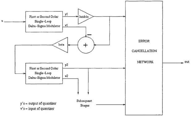
An alternative solution to the stability problem is to instead use multi-stage noise shaping (MASH) and cascade stable first or second order single-loop structures, as shown in Figure 1.3. The output of one stage becomes the input to the next stage after passing through what is known as an "error mixing network." Lambda is the error mixing
y First or Second Order lambda
v': = Single-Loop
Delta-Sigma Modulator Y1
-beta- :
y2
First or Second Order
: Single-Loop Q
Delta-Sigma Modulator v
y's = output of quandizer Subsequent
v's = input of quantizer tae
- out
Figure 1.3: MASH Delta-Sigma Modulator
coefficient, and beta is the error gain coefficient. Notice that if lambda=1, the input to the next stage is simply a scaled version of the quantization error of the previous stage. To eliminate the noise due to the additional quantizers, such cascaded structures also require
ERROR
CANCELLATION
error cancellation circuitry, or filters which are designed to cancel out the quantization noise of subsequent stages.
The chief problem with cascaded architectures, however, is that they can be more sensitive to capacitor mismatch errors and other non-idealities. Any error in the coefficients of the error cancellation circuitry result in the increase of the quantization noise that is seen at the output.
1.2
Background Research
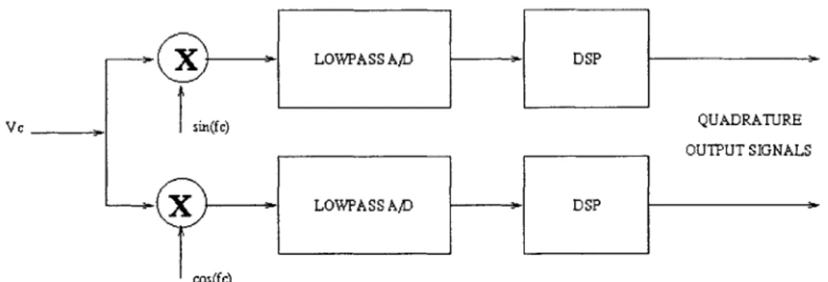
The motivation for this research stems from the need at Draper Laboratory for an A/D converter with good resolution and high dynamic range to process the narrowband output signal of a precision sensor. There are three principle ways of approaching the conversion of a narrowband signal. One way is to mix the signal down to DC, and then perform lowpass delta-sigma modulation (Figure 1.4). The chief problem with this approach, however, is that the output is susceptable to drift in the DC value of the input to the A/D converter as well as to 1/f noise.
Another approach is to apply a low pass delta-sigma conversion prior to demodulation (Figure 1.5). However, this is not the optimal approach for processing the narrowband signal because the noise in the band of interest may only experience moderate suppression. Such designs have provided reasonable performance, but have not yet met the desired noise level specifications.
- LOWPASS AjD DSP
Vc sin(fc) QUADRATURE
OUTPUT SIGNALS
X
LOWPASS AAD DSPcos(fc)
Figure 1.4: Narrowband Signal Processing: Mix signal down to DC, then use lowpass modulator
X -I DSP
Vc LOWPASS AID sin(f ) QUADRATURE
OUTPUT SIGNALS
X) DSP
cCos(fc)
Figure 1.5: Narrowband Signal Processing: Directly convert signal with lowpass modulator
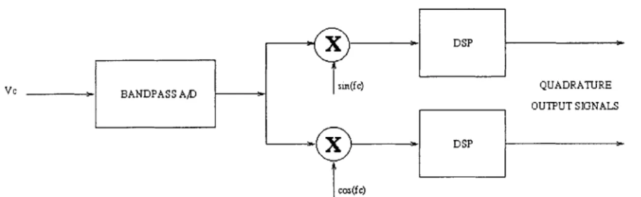
A third way of processing the signal is to use a bandpass delta-sigma converter (Figure 1.6), which takes advantage of the narrowband nature of the signal to improve performance and power dissipation.
X DSP
Vc BANDPASS A/D sin(fc) QUADRATURE
OUTPUT SIGNALS
X 4DSP
cos(fc)
Figure 1.6: Narrowband Signal Processing: Directly convert signal with bandpass modulator
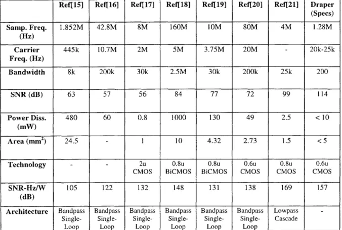
Previous delta-sigma designs at Draper Laboratory have all utilized the second conversion method: direct application of a lowpass delta-sigma converter. Indeed, much of the literature focuses on lowpass delta-sigma conversion using a single-loop topology. However, cascaded architectures have gained increasing attention. A 1994 work by David Ribner [10] introduced bandpass cascaded architectures at a theoretical level, and comparative studies on a MATLAB level of the influence of non-idealities and quantization noise have been done by other researchers [11, 12, 13, 14]. The performance of some verified modulator designs and their performance is summarized in Table 1. The modulator requirements of Draper Laboratory are also included. As a basis
for comparing modulators, a performance factor based on Signal-to-Noise Ratio (SNR), bandwidth, and power consumption was devised:
SNR-Hz/W = SNR + 10 log(Bandwidth) - 10 log(Power Dissipation)
Table 1: Summary of Past Modulator Designs
(1.3)
Ref[15] Ref[16] Ref[17] Ref[18] Ref[19] Ref[20] Ref[21] Draper (Specs) Samp. Freq. 1.852M 42.8M 8M 160M 10M 80M 4M 1.28M (Hz) Carrier 445k 10.7M 2M 5M 3.75M 20M - 20k-25k Freq. (Hz) Bandwidth 8k 200k 30k 2.5M 30k 200k 25k 200 SNR (dB) 63 57 56 84 77 72 99 114 Power Diss. 480 60 0.8 1000 130 49 2.5 < 10 (mW) Area (mm2 ) 24.5 - 1 10 4.32 2.73 1.5 < 5
Technology - - 2u 0.8u 0.8u 0.6u 0.8u 0.6u
CMOS BiCMOS BiCMOS CMOS CMOS CMOS
SNR-Hz/W 105 122 132 148 131 138 169 157
(dB)
Architecture Bandpass Bandpass Bandpass Bandpass Bandpass Bandpass Lowpass
-Single- Single- Single- Single- Single- Single- Cascade
1.3
Thesis Objective
The objective of this thesis is to further explore bandpass delta-sigma conversion, and in particular MASH architectures, in light of the system requirements of Draper Laboratory. Thus, two architectures are considered in this work:
1. A fourth order single-loop bandpass delta-sigma modulator; and 2. A fourth-order 1-1 cascaded bandpass delta-sigma modulator.
Both are analyzed with regards to their design issues, and the effects of non-idealities, in particular capacitor mismatch and finite operational amplifier gain.
CHAPTER 2
A 4-TH ORDER SINGLE LOOP A-X MODULATOR
2.1 Topology
A block diagram for the 41h order single loop architecture is shown in Figure 2.1. From this block diagram, the NTF for this architecture can be found to be
N =Z2 +(gc, - 2)z+ lz2 +(g 2c3 2)z+1 (2.1)
z4 +kz 3 +ksz 2 +k3z+k4
where
k =g 1c, + g 2c3 -4+c 4[a4 +ac 3]
k2 =2+(g~c, -2)(g 2c3 -2)+c 4[cc 3(a2 +ac,)+(gc, -2)(a 4 +a3c3)-a4]
k3= g1c + g2c3 -4+c 4[a4 +a3c3 - c2c3a2 -a4(c 1 -2)]
k4 -1- c4a4
The primary consideration in selecting the modulator coefficients is choosing the NTF such that the in-band SNR is maximized. As can be observed from the NTF expression, for bandpass modulators, NTF zeros come in complex conjugate pairs. As a result, only even-order bandpass systems are realizable. One possible choice is to place all the NTF zeros in the center of the band. In this case, high SNR is achieved near the center frequency, to the detriment of system performance at the fringes of the band. For
hi h23h
-gl g2
z/zl l1(-) c2 z/(z- 1) - 3 (--M) -- c4 Quantizer
-al T -2 -a3 -a4
wideband systems, this is not an optimal placement. If the zero pairs are separated, and placed away from the center, then the performance at freqencies at the fringes of the band is improved at the expense of performance near the center of the band. At a certain point, for each system, there is an optimal placement of poles away from the center. For small bandwidth systems, however, coincident zeros at the center frequency yield optimal performance because most the input signals are concentrated at the center frequency anyway.
The narrowband system required by Draper Laboratory has a bandwidth of 200Hz. Thus, all NTF zeros were placed at the center frequency of 20kHz. To facilitate the design of the remaining modulator coefficients, a Delta-Sigma Toolbox developed by Richard Schreier for MATLAB was used. A description of the Toolbox commands used is included in Appendix A. In this way, a set of coefficients that realizes the desired NTF with unity STF was computed. However, to ensure correct operation of the modulator, the integrators must not be saturated. Thus, the modulator coefficients must then be scaled according to the input amplitude range to prevent clipping. This was again accomplished using MATLAB to yield the following modulator coefficients and NTF:
al=0.3964 a2=0.3754 a3=0.4079 a4=0.3890 b1=0.3964 b2=0.3754 b3=0.4079 b4=0.3890 b5=1 cl=0.0863 c2=0.2361 c3=0.4242 c4=1.4277 gi=0.1116 g2=0.0227 NTF= (z2 -1.99z +1)2 (2.2) (z2- 1.491z + 0.5652)(z 2 - 1.687z + 0.7865)
2.2
Predicted SNR
A primary performance measure of A/D converters is the signal-to-noise ratio (SNR). The SNR is defined as the ratio of the output signal power to the noise power. Consider the SNR calculation for an L-th order real bandpass delta-sigma modulator with an input signal band of ±fB about a carrier fc and a sampling rate of fs.
SNR =l0 log x (2.3)
where y2 is the input signal power and Gey2 is the in-band noise power at the output.
Under the unity gain approximation, the quantizer error, e[n], is modelled as white noise. Further assuming that the modulator output is filtered by an ideal bandpass filter (to remove all out-of-band noise), the in-band noise power can be expressed as
2
- Hed
(f)|fdf
(2.4)band fs
2 2
where -= and V is the amplitude of the input sinusoidal signal.
3
Using these two equations, the SNR ratio for any system, given the NTF, He, can be found. A detailed derivation of the SNR for an Lh -order bandpass modulator can be found in [22] to yield the following result:
3a2(L+1)(2R) L± dB (2.5)
SNR =l10log t) 4k ,, d 25
2)T~
where L is the order of the modulator, and R is the oversampling ratio (fs/2fb),
k = 1, and (o0 and (% are the center frequency and bandwidth (in
L(L - 1) ...1 d AOL
radians) respectively.
To calculate the expected SNR of the 4th order modulator specified in the previous
section, a MATLAB function called Predict4.n was written. Using Predict4.m, the expected SNR at the output is computed to be 185.8 dB. The code for Predict4.m is included in Appendix B.
Note that these SNR predictions consider the noise due to quantization noise only. In an actual implementation of a delta-sigma modulator, other circuit noise sources also factor into the overall SNR. However, for the purposes of comparing the single loop and cascaded architectures, only the SNR due to quantization noise is considered.
2.3 Capacitor Mismatch and Finite Op Amp Gain
Typically the integrators of the modulator are implemented using switched capacitor circuitry. An implementation of z/(z-1) is shown in Figure 2.2 and an implementation of 1/(z-1) is shown in Figure 2.3. Note that these circuits are identical except their sampling clocks are reversed.
To assess the effects of finite op amp gain and capacitor mismatch, the transfer function for the overall circuit must be computed in terms of the op amp gain (A) and the
capacitor values. The assumptions about the op amp used in this calculaton are discussed in the next section.
c2
Phi2 hi Sample on PEIl
Figure 2.2: Switched Capacitor Implementation of z/(z-1)
c2
P i g 2p l ai
S a m p l e
o f P hi
Figure 2.3: Switched Capacitor Implementation of 1/(z-1)
2.3.1 Op Amp Modeling
An ideal op amp is modelled as having a constant, but very large, open loop gain A, such that the output of the op amp, V,, is related to its input voltages, V_ and V, by
V = A(V+ -V ) (2.6)
This equation, however, ignores the frequency dependency of the op amp gain. A typical op amp has a very large gain at DC, and at the -3dB frequency (which defines the bandwidth of the op amp) begins to roll off at -20 dB/decade, until finally dropping to unity at the crossover frequency. Once past the crossover frequency, the gain falls further and additional high frequency poles cause the gain to roll off faster. The phase of the op amp is also not a constant. At DC, the phase is zero, whereas by the crossover frequency the phase is at least -90'. Beyond crossover, higher frequency poles cause the phase to shift even more negative.
A key performance factor of an op amp is its gain-bandwidth (G-B) product. Because the G-B product is a constant at a particular temperature, an op amp with a high DC gain has a smaller bandwidth than an op amp with a low DC gain. Depending on the design of the op amp then, the system may either be operating in the constant gain region below the 3 dB frequency, or in the 20 dB rolloff region between the 3 dB and crossover frequency. Thus, when assessing the effects of finite op amp gain, the gain that must be considered is not the DC gain A, but the gain at the operating frequency A(fe). In simulations, A(fc) will be considered to vary from as low as 100 to as high as 5,000 and for simplicity, the phase is assumed to be zero.
2.3.2 Transfer Function Considering Non-Idealities
With this op amp model in mind, the transfer function for the implementation of z/(z-1), the circuit of Figure 2.2, in terms of capacitor ratios and op amp gain can be found to be V", (z) V, (z) AC1 zI c C 1 Az z C1 +(1+ A)C(1+A)C2 C,
2 -+ - when A goes to infinity
C_ (1+A)C2 Z-1 I-z
CI +(I+ A)C2
(2.7)
Similarly, the transfer function for the implementation of 1/(z-1), the circuit of Figure 2.3, is found to be - AC, VC,,(z) C, +(1+A)C 2 V, (Z) _ (1+ A)C 2 Z-1 CI + (I+ A)C2 C' C,
--+ -when A goes to infinity. 1 -z
By adjusting the state-space equation coefficients according to the transfer functions derived above, the effects of non-idealities are introduced in the MATLAB simulations. The results of such simulations are presented in Chapter 4.
25
CHAPTER 3
A 4-TH ORDER 1-1 MASH A-1 MODULATOR
3.1
Topology
A block diagram for the 4th order 1-1 MASH architecture is shown in Figure 3.1. The structure consists of two cascaded 2 order single loop structures. However, the arhitecture is known as a 1-1 MASH because each stage contains one resonator in the forward path. In general, the two stages can have different modulator coefficients. However, in this system, because both stages are being sampled at the same rate, identical second order stages were used.
Using an approach identical to that used in the design of the 4'h order single loop
modulator, the coefficients for the 2nd order sections comprising each stage of the MASH
architecture were designed to be:
at = a3 =0.4846 a2 = a4= 0.1261
b, =b 4= 0.4846 b2 = b5= 0.1261 b3 = b6 = 1.0000
C = c3 = 0.0992 c2 = c4 = 4.4286 g = g = 0.0971
which gives a noise transfer function of
NTF = z2 -1.99z +1 (3.1)
To prevent saturation of the second stage, k and
P
were chosen to be 1 and 0.8, respectively. -I--'I <1 + + + 0 -o 0 I-273.2 Error Cancellation Filter Design
3.2.1 Exact Noise Cancellation
The error cancellation filters, HI and H2, are designed such that the quantization
noise from the quantizer of the first stage is cancelled. Again, using the unity gain approximation, the following relations can be found from the block diagram:
STFn NTFn Y, = U + N El (3.2) STFd NTFd STFn NTFn E (3.3) Y, = U2 + E33 STFd NTFd
U2 =(AY V-v)=9[(A- I)i' -FE,] (3.4)
OUT = HY +H 2 Y2 (3.5)
where U, U2, Y1, Y2, V1, OUT,
P
and X are as indicated in Figure 4.1; STFn and STFdare the numerator and denominator polynomials of the STF respectively; NTFn and NTFd are the numerator and denominator polynomials of the NTF respectively, and El and E2 are the power spectral densities of the quantization error of the first and second stage quantizers respectively.
From these equations, OUT can be calculated in terms of U1, E and E2:
OUT =H +(-1) STFn H Fn U (3.6)
STFd 2 STFd
STFn NTFn STn ~ NTFn
+ [H +(A-1) H ,+ H E + H E
However, because the STF is designed to be 1 this equation reduces to
F
NTFn OUT = (H, + I-1)H 2)U + (H, +#(2 -)H2)L
NTFd +1#H2 E NTFn + H 2E2 NTFdTo cancel the quantization noise from the first stage quantizer, the coefficient of El is set to zero to yield the following requirement on H, and H2:
(HI +6(A -1)H2)NTFn+#3(NTFd)H2 =0 (3.8)
Substituting the expressions for the NTF, this equation can be solved to find the H2 required for exact noise cancellation in terms of HI:
H2C# 1+k z' 3 +z2
H
(3.9)where NTFn= 1 +k3z'+z2 and NTFd=1+klz +k2z
2 . one obvious choice for H1 and H2 would be:
H =-#(1+(k, +(A-1)k3)Z~'+(k2+/-_)Z-2 )
From this equation, we can see that
and H2 =1+k3z- +z-2 (3.10)
To calculate the SNR predicted by the theory, a MATLAB function called
Model.m was written. This function takes as an input a sinusoid at the center frequency
29
and processes it according to the block diagram and the unity gain approximation: the input signal is filtered by the STF and NTF of each stage to compute Y and Y2, which
were then filtered by H1 and H2 and summed to compute the overall modulator output,
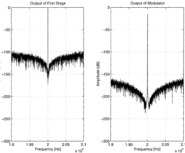
OUT. Using Model.m, the expected SNR at the output is computed to be 193 dB. A plot of the output of the first stage and the modulator is shown in Figure 3.2.
Output of First Stage
0 -50 100 co 0 -0-E 150 -200 -250 Output of Modulator -. -. -. . .- -F -..-.--.-.-.-.-.--3001 9 1.95 2 2.05 2.1 1.9 1.95 2 2.05 2.1 Frequency [Hz] X 104 Frequency [Hz] x 104
Figure 3.2: Power Spectrum of I" Stage and Modulator Output Signals for Exact Error Cancellation Filters
0 -50 -100 0 -S-150 E -200 -250--. u 1 . -.. .. .
-. ....
A-A -.. . . . -. . --. -. . . .- ..- .- . -.The chief problem with this selection of filters, however, is apparent from the spectrum of the modulator output: the noise is suppressed to levels at about -210 dB, but signal amplitude as also been attenuated by about 20 dB! The reason for this can be seen from the equation for OUT: for X=1, the coefficient of U is H1. Because H, is itself a
filter which attenuates in-band frequencies, the input signal is also attenuated.
To avoid this problem, H, should be set to a unit delay. In this case, an exact cancellation of the quantization error requires that H2 be an Infinite Impulse Response
(IIR) filter. However, using an IIR filter in the error cancellation network results in a continuous, as opposed to quantized output, because the output can then take on values in between the quantization levels. To preserve the quantized nature of the output, H2 must
be selected to be a Finite Impulse Response (FIR) filter.
However, there is no FIR filter for H2 that can exactly satisfy equation (3.8) when
H1 is selected to be a unit delay!
Thus, the design of H2 reduces to a minimization problem: given that the error
cannot be totally cancelled, what filter minimizes this error? There are many possible filters that could be designed in answer to this question. This study looks at two design approaches: one based on modelling the system in the frequency domain, and one based on modelling the system in the time domain.
3.2.2 Frequency Response Approximation
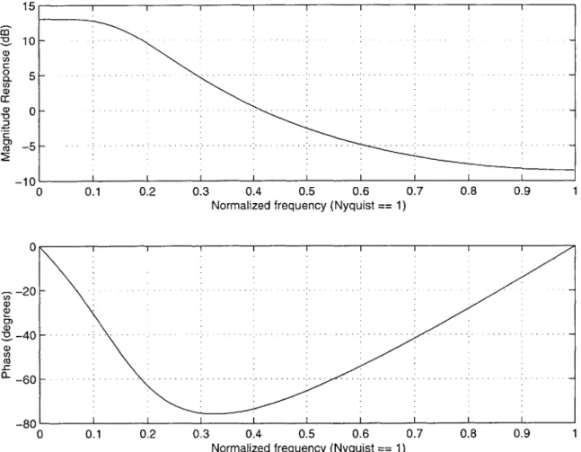
One way to approach this problem is to model the frequency response of
P = I
2+ (k, + (-)k 3 )Z-' + (k2 + )z-2
response is shown in Figure 3.3.
as an FIR filter. A plot of the frequency
0 0.1 0.2 0.3 0.4 0.5 0.6 0.7 0.8 0.9 1
Normalized frequency (Nyquist == 1)
0.1 0.2 0.3 0.4 0.5 0.6 0.7 0.8 0.9 1
Normalized frequency (Nyquist == 1)
Figure 3.3: Freqency Response of P(z)
15 10 5 0 -5 0 0. (n) 0) 0) - . . . . . - . .. . . . --. -. .. . . . . -10 C 0) -2( -4C (-CL -U -80 0 - . . .. . . - - ... ... - ... .- -.. ... . .. ... -- -- .... - -...- ...- .- ...-. - -. ...-. . ....- - ..
-From this plot it can be observed that the magnitude of P(z) is essentially constant in the frequency band of interest. Approximating P(z) as a constant gain (henceforth referred to as the Gain Model) H2can be found to be
H2 ~K
(I+
k z-' + z-2)H where K is a constant.From the magnitude plot of the frequency response, K was found to be 4.5, giving error cancellations filters of
HI = z ' and H2 = -5.625z ' +11.196z 2 -5.625z<
(3.12)
With this selection of error cancellation filters, Model.in computes the SNR to be 145 dB. A better approximation that adds a minimal amount of complexity involves also taking into account the phase information of the frequency response (Gain-Phase Model). At low frequencies, the phase drops linearly. Modeling P(z) as Kz-I leads to error cancellation filters of
HI = z-1 and H2 =
-5.625z-2+11.196z -5.625z (3.13)
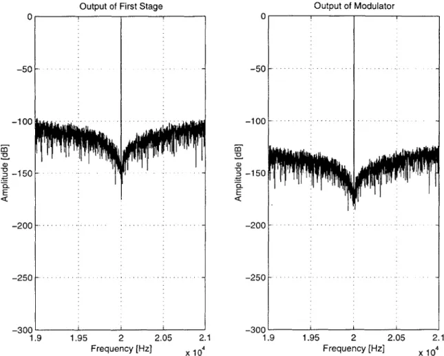
With these error cancellation filters, Model.m computes the SNR to be 149 dB over a 200 Hz bandwidth - a 5 dB improvement over the Gain Model for P(z). A plot of the ideal performance with this selection of error cancellation filters is shown in Figure 3.4.
33
Output of First Stage 2 2.05 2. Output of Modulator 0 -50 -100---- - - - -- -:3-150 E -200 -. - . - .- .--250 --300 1 1.9 1.95 2 2.05 2. Frequency [Hz] x 104 Frequency [Hz]
Figure 3.4: Power Spectrum of 1" Stage and Modulator Output Signals
Using Gain-Phase Model
0 -50 100 150 E E
-$-w-.-.
-200 F --. -. -250 k -300' 1. 1.95 x 10⁴ ' '_ - ' ....-.-...-.-.-. ---- --....
9 13.2.3 Impulse Response Approximation
Another design approach involves using the impulse response of P(z) to approximate P(z) as an FIR filter. A plot of the impulse response of P(z) is shown in Figure 3.5. From this plot, it can be observed that altough P(z) is an IIR filter, after a delay of 17 units, the response has died down so that P(z) can be well represented by
17 P(z) ~Iki z~(3.14) n=O Impulse Response 1.21 - 0.8- 0.6- 0.4- 0.2- 0-0 5 10 15 20 25 Time (samples)
Figure 3.5: Impulse Response of P(z)
35 a) E .... .. ... ...... .... ... - - - . . .. .. ..-. . ..-. . ..-. . ..-. ...-. -.. . . .-. .- .. ..-. . .-. .. -. ...- . - -. .. .. .-. . . . ... .-.. . .-.. .-.. .-.. .-.-.. - - . ... -...-. -.... ....- -... -...- ... -..... . .. . ...- .. . . ..-. . -. . -..- .- ..- ..- ..
--The coefficients kn can be directly read off from the impulse response plot. If P(z) is approximated with all 18 coefficients, the result will be very good - near exact - error cancellation. Choosing fewer coefficients may result in a simpler system, but is also a poorer approximation of the impulse response.
To get an idea for the tradeoff between complexity and performance, the SNR was computed using Model.m for n=1 to n=17. The results are shown in Table 2.
n Tier 1: 2 3 4 Tier 2: 5 6 7 8 9 10 Tier 3: 11 12 13 14 15 16 17
Table 2: SNR Calculated for Varying
SNR fdBl 135 137 142 150 163 163 159 160 163 167 181 181 196 186 185 187 189 Filter Lengths
From the table we can observe roughly three levels of performance (labelled as Tiers 1, 2 and 3). The filters in Tier I have the lowest order. While being simpler in that filters with less coefficients generally require less hardware to implement them, these
filters do not perform well in comparison with the Gain-Phase Model based filter presented in the previous section.
The performance of the Tier 2 filters is better than that of the Gain-Phase Model filter, and has an SNR 20 dB higher than the filters in Tier 1. By moving up to the Tier 3 filters, those that use the most coefficients of the impulse response, results very close to those that would have been attained with the exact error cancellation filter, had not the signal level also been attenuated, are achieved.
3.2.4 Error Cancellation Filter Selection
The design of error cancellation filters involves a tradeoff of performance with efficiency and robustness. Higher order filters have better SNR performance, but also generally require more hardware to implement, thereby increasing the power consumption of the overall system. Additionally, systems using error cancellation filters with more coefficients are generally also more sensitive to capacitor mismatch variations than those that use filters with fewer coefficients, because more parameters are being affected by the
non-ideality.
For the purposes of this study, the primary MASH architecture considered utilizes the Gain-Phase Model based error cancellation filters:
HI = Z' -1 and H2= -5.625z-2 +11.196z -5.625z- 4 (3.15)
However, because the Tier 3 filters are expected to yield SNR performance comparable to that of the single loop architecture, the error cancellation filter designed for the model with n=17 is also considered:
HI = z and H= =-I.25z~' + 0.9642z-2 + 0.4773z-' + 0.156 1Z 4 - 0.0205z~' - 0.0939z-6 -0.1054z--7 - 0.087z - 0.0596z-9 - 0.0342z<O - 0.0154z<" -0.0036z-12 +0.0024z1 +0.0045z~4 +0.0044z-" +0.0034z-6 +0.0022z-' 7 +0.0039z-" -0.0029z-'9 (3.16)
CHAPTER 4
SIMULATION RESULTS
4.1 Single Loop Architecture
4.1.1 Simulated Performance
MATLAB was used to simulate the modulator and test performance. All MATLAB code used for simulating the single loop architecture is included in Appendix B. The bulk of the code consists of using iteration to compute the output sequence given a sinusoidal input sequence. The quantizer is implemented as a comparator.
The SNR of the modulator is calculated by using a test input sinusoid of 20kHz (the center frequency). The power spectrum of the output sequence is calculated. The SNR is given by the difference in decibels of the signal amplitude and the in-band noise. Thus, the SNR is found to be 186.4 dB in a 200 Hz bandwidth.
This simulation result compares well with the 185.8 dB SNR predicted earlier.
4.1.2 Effects of Capacitor Mismatch
To assess the effects of capacitor mismatch and finite op amp gain, the equations derived in the previous chaper were coded into MATLAB. Assuming an op amp gain of 1,000,000, capacitor mismatch variations were added to the nominal values. For
variations of 10-4 (+/- 1% la), 10-6 (+/- 0.1% 1(), and 10-8 (+/- 0.01% l) the system was
tested over 100 runs, for which the SNR was recorded each time. The graph in Figure 4.1
summarizes the results of the data. The individual histograms from which this plot was generated are included in Appendix D.
185
184
183 10
Average, Minimum, and Maximum Output SNR vs Capacitor Mismatch Variance Average - -- - Minimum Maximum... -X -.. . -. . . . .. . .-. ..-. ..-... .. . -. --. -. . . .. . . . .-. .-.-. .-. .-.--. . .. . . .. . .. . -. -. -. . .. - --. -8 10-7 10-6 10-5
Capacitor Mismatch Variance
104 10-3
Figure 4.1: Capacitor Mismatch Simulation Results for Single Loop Architecture
190 189 188; 187 V z Cl) 186 . -1 1 1 1 1 L
4.1.3 Effects of Finite Op Amp Gain
The effects of finite op amp gain was determined by calculating the SNR of the modulator for the following gains: 100, 300, 600, 1000, 3000, 5000, and 10000. The results of these simulations is plotted in Figure 4.2.
This plot demonstrates that in order to achieve near the ideal performance of the modulator, the op amp gain at the operating frequency must be kept above about 3,000.
Single Loop Modulator Output SNR vs Op Amp Gain 190 180 170 160 150 140 130 120 110 0 1000 2000 3000 4000 5000 Op Amp Gain 6000 7000 8000 9000 10000
Figure 4.2: Plot of Single Loop Modulator SNR With Varying Op Amp Gain
41 -I - - - - -- ...- . -. .
....
.. . . .. - -...4.2 MASH Architecture
With the same methodology as applied for the single-loop modulator, MATLAB simulations were conducted to evaluate the performance of the MASH architecture.
4.2.1 Gain-Phase Model Simulation Results
With ideal integrators, the SNR is found to be 157 dB over a 200Hz bandwidth, a result better than that predicted in Chapter 3. This is because the calculation performed by Model.m uses the unity gain approximation. As mentioned in Chapter 1, the unity gain approximation is not a very good model of a 1-bit quantizer because it does not have many levels. Because the Gain-Phase Model does not attempt to exactly cancel the noise, however, the system still performs well, and indeed exceeds expectations.
The results of the capacitor mismatch simulations and finite op amp gain simulations are shown in Figures 4.3 and 4.4, respectively. Histograms of the capacitor mismatch Montecarlo simulations are included in Appendix D.
4.2.2 Simulation Results for Model with n=17
With ideal integrators, the SNR is found to be 160.8 dB over a 200Hz bandwidth. This result is drastically poorer than that predicted by Model.m (-190 dB). One reason for this has already been mentioned: the unity gain approximation is not a very good model of 1-bit quantizers. The n=17 Model attempts to precisely cancel an error which cannot even be accurately determined by the unity gain approximation. As a result, what seems in
Average, Minimum, and Maximum Output SNR vs Capacitor Mismatch Variance Average - -- Minimum --- Maximum ... ...- ... .. --. .. -7
-. ...
-.
...
-..
-..
.
...
..
-..
-
...
...
... .
-
.
...
-..
-.
-.
..
-.
...
.-.-.
.-.
-
.--.
-.
...
..
-.
....
10-7 105Capacitor Mismatch Variance
10-4 10-3
Figure 4.3: Capacitor Mismatch Simulation Results for MASH Architecture (Gain-Phase Model)
43 153.5 153 152.5 152 51.5 1 V cr z (I) 151 150.5 150 149.5 149 148.5 10 -8 10-6
MASH Modulator Output SNR vs Op Amp Gain 150 140 130 -0 1000 2000 3000 4000 -4 P o M M (Gai-P M SNR s~~ . .q~ ~ . -..
Figure 4.4: Plot of MASH Modulator (Gain-Phase Model) SNR
With Varying Op Amp Gain
5000 6000 7000 8000 9000 10000 Op Amp Gain 190 180 170 160 M z C/) -. . -. -. -. / I I I I I I I 120 11C
theory to be a more accurate and precise error cancellation filter, is in fact, a much poorer design.
Capacitor mismatch montecarlo simulation results show that for a capacitor mismatch variance of 0.0001, the output SNR varies between 156.3 dB and 183.4 dB with an average SNR of 168.7 dB. The histogram giving this result is included in Appendix D.
The results of the op amp gain variation simulations are illustrated in Figure 4.5.
190 180- - 170-160 150 ---140 -130 -120 110
MASH Modulator Output SNR vs Op Amp Gain
0 1000 2000 3000 4000 5000 6000 7000 8000 9000 10000
Op Amp Gain
Figure 4.5: Plot of MASH Modulator (Model with n=17) SNR With Varying Op Amp Gain
45 Vr z U) -.
-- / -... ... -.. .. . - . . .
4.3 Summary of Results
Table 3 summarizes the results of the simulations presented above. For ease of comparison the predicted results computed in previous chapters are also included.
Predicted SNR Simulated SNR SNR Variation SNR Variation
(dB) (dB) Given Cap. With Finite Op
Mismatch (dB) Amp Gain (dB)
Single Loop 186 186 184-189 127-182 Modulator Gain-Phase 149 157 148-153 114-151 MASH Modulator n=17 Model 189 160 156-183 114-145 MASH Modulator
Table 3: Summary of Predicted and Simulated Results
From these results it can be seen that in terms of SNR performance, the Single Loop Modulator clearly performs better than the MASH Modulator. While using more error cancellation filter coeffients in theory gives as high an SNR as the Single Loop Modulator, in actuality the limitations of the unity gain approximation cause the MASH modulator to yield relatively poorer SNR performance.
In terms of robustness, both architectures perform comparably. The Single Loop Modulator and Gain-Phase MASH Modulator vary by only 5 dB with capacitor mismatch variation. For op amp gains greater than roughly 8000 the effect of gain variation on SNR performance is also insignificant.
As expected from the analysis in Chapter 4, the n=17 Model MASH Modulator is much more sensitive to capacitor mismatch variations than the Gain-Phase MASH Modulator. The SNR performance is quite unstable, with a variation of 27 dB! Additionally, the n=17 Model MASH Modulator performance is also more negatively impacted by low op amp gain. With a gain of 10,000 the SNR is still 15 dB less than the ideal simulated SNR.
CHAPTER
5
CONCLUSION
The performance of two 41h order delta-sigma A/D topologies were analyzed: that of a single loop modulator, and that of a MASH modulator. MATLAB simulation results showed that given the same sampling frequencies, the single loop modulator yielded a higher SNR than the MASH modulator. Both architectures performed comparably with regards to robustness. However, MASH designs with higher order error cancellation filters are very sensitive to capacitor mismatch variations and finite op amp gain non-idealities.
The reason for the poorer SNR performance of the MASH architecture involves a fundamental design issue of MASH modulators: designing an error cancellation network that can accurately cancel the first stage quantizer error. Several possible cancellation filter design approaches were presented. However, because of the limitations of the unity gain approximation, error cancellation filters designed based on this approximation do not yield good results.
Once possible way of improving MASH architecture performance involves using a more accurate quantizer model based on describing functions. The design of delta-sigma modulators using model that combines describing function analysis, analytical modeling, and empirical approximation (Adaptive Gain Model) was presented by Louis Williams in his 1993 Doctoral Thesis [4]. In that work the Adaptive Gain Model was used to design a 3rd order 2-1 lowpass cascaded architecture. Use of such a model was
shown to yield results that allowed for the prediction of other effects such as the overload performance of the modulator. However, such an analysis is quite involved. More work needs to be done to further develop such methods.
Another method of improving MASH architecture performance involves using a multi-bit quantizer in the second-stage, and thereby better satisfy the requirements for the unity gain approximation. The key concern in using multi-bit quantizers, however, is linearity. While with 1-bit quantizers the quantizer is ensured to preserve the linearity of the system, the use of multi-bit quantizers introduces additional errors and distortion from the quantizer. Applications with stringent linearity requirements seem to preclude the use of multi-bit quantizers. However, if the first stage is designed with a 1-bit quantizer, and only the second stage uses a multi-bit quantizer, then performance can be achieved with minimal effects on linearity: because the input signal of the second stage is a signal on the order of the quantizer error (i.e. small amplitude), the distortion introduced by non-linearity in the second stage quantizer is correspondingly smaller.
In conclusion, while MASH architectures designed with the conventional unity gain approximation of the quantizer do not yield as good SNR performance as a single loop design, future work on the design of error cancellation filters and quantizer modeling may enable better and more comparable MASH modulator designs.
APPENDIX A
Delta-Sigma Toolbox for MATLAB
MATLAB's internal representation of the modulator is accomplished using the ABCD matrix. The ABCD matrix is essentially the state-space description of the modulator, and stores in matrix form the following equations:
x(n+1) = Ax(n) + B[u(n) v(n)]' y(n) = Cx(n) + D[u(n) v(n)]'
where x is the vector of state variables, y is the input to the quantizer, u is the input of the modulator, and v is the output of the modulator (and quantizer).
Thus, the ABCD matrix becomes
ABCD = [A B ; C D] using MATLAB notation.
The following is a list of the Toolbox functions utilized in designing the modulator.
A.1 SynthesizeNTF
ntf = synthesizeNTF(order=3,R=64,opt=O,H_inf=1.5,fO=O) Synthesize a noise transfer function for a delta-sigma modulator.
order = order of the modulator
R = oversampling ratio
opt = flag for optimized zeros
0 -> not optimized,
1 -> optimized,
2 -> optimized with at least one zero at band-center H_inf = maximum NTF gain
fO = center frequency (1->fs)
A.2 PredictSNR
[snr,amp,kO,k 1 ,sigma e2] = predictSNR(ntfR=64,amp=...,fO=0)
Predict the SNR curve of a binary delta-sigma modulator by using the describing function method of Ardalan and Paulos.
The modulator is specified by a noise transfer function (ntf). The band of interest is defined by the oversampling ratio (R) and the center frequency (fM).
The input signal is characterized by the amp vector.
amp defaults to [-120 -110...-20 -15 -10 -9 -8 ... 0]dB, where 0 dB means
a full-scale (peak value = 1) sine wave.
The algorithm assumes that the amp vector is sorted in increasing order; once instability is detected, the remaining SNR values are set to -Inf. Output:
snr a vector of SNR values (in dB) amp a vector of amplitudes (in dB) kO the quantizer signal gain ki the quantizer noise gain
sigmae2 the power of the quantizer noise (not in dB)
The describing function method of A&P assumes that the quantizer processes signal and noise components separately. The quantizer is modelled as two (not necessarily equal) linear gains, kO and kl, and an additive white
gaussian noise source of power sigma_e2. kO, kl and sigma-e2 are calculated as functions of the input.
The modulator's loop filter is assumed to have nearly infinite gain at the test frequency.
A.3 RealizeNTF
[a,g,b,c] = realizeNTF(ntf,form='CRFB',stf=1)
Convert a noise transfer function into coefficients for the desired structure. Supported structures are
CRFB Cascade of resonators, feedback form. CRFF Cascade of resonators, feedforward form. CIEFB Cascade of integrators, feedback form. CIFF Cascade of integrators, feedforward form.
CRFBD CRFB with delaying quantizer.
See the accompanying documentation for block diagrams of each structure The order of the NTF zeros must be (real, complex conj. pairs).
The order of the zeros is used when mapping the NTF onto the chosen topology.
A.4 StuffABCD
ABCD = stuffABCD(a,g,b,c,form='CRFB')
Compute the ABCD matrix for the specified structure. See realizeNTF.m for a list of supported structures. mapABCD is the inverse function.
A.5
MapABCD
[a,g,b,c] = mapABCD(ABCD,form='CRFB')
Compute the coefficients for the specified structure. See realizeNTF.m for a list of supported structures. stuffABCD is the inverse function.
A.6 ScaleABCD
[ABCDs,umax,S]=scaleABCD(ABCD,nlev=2,f=O,xlim=1,ymax=nlev+5,umax,N=le5) Scale the loop filter of a general delta-sigma modulator for dynamic range.
ABCD The state-space description of the loop filter. nlev The number of levels in the quantizer.
xlim A vector or scalar specifying the limit for each state variable.
ymax The stability threshold. Inputs that yield quantizer inputs above ymax are considered to be beyond the stable range of the modulator.
umax The maximum allowable input amplitude. umax is calculated if it is not supplied.
ABCDs The state-space description of the scaled loop filter.
S The diagonal scaling matrix, ABCDs = [S*A*Sinv S*B; C*Sinv D];
A.7 CalculateTF
[ntf,stf] = calculateTF(ABCD,k=l)
Calculate the NTF and STF of a delta-sigma modulator whose loop filter is described by the ABCD matrix, assuming a quantizer gain of k. The NTF and STF are zpk objects.
APPENDIX B
MATLAB CODE FOR SINGLE LOOP MODULATOR
SIMULATIONS
B.1 Code for Calculating Expected SNR
%%%%% PREDICT4.M %%%%% N=16*64*2048; fs=2*200*3200; time= [1:N] /fs; fin=20000; in=1; u=in*cos(2*pi*fin*time); e1=2.5*(rand(1,N)-0.5); stfn=[1]; stfd=[1]; ntfn=conv([1 -1.99 1],[1 -1.99 1]); ntfd=conv([1 -1.491 0.5652],[1 -1.687 0.7865]); al=0 .3964; a2=0 .3754; a3=0 .4079; a4=0 .3890; gl=0.1116; g2=0 . 0227; bl=0.3964; b2=0 . 3754; b3=0.4079; b4=0 .3890; b5=1; c1=0 .0863; c2=0.2361; c3=0.4242; c4=1 .4277; newntfn=[1 (g1*c1+g2*c3-4) (g1*c1-2)*(g2*c3-2)+2 (g1*c1+g2*c3-4) 1]; const1=g1*c1+g2*c3-4+c4*(a4+a3*c3); const2=2+(g1*c1-2)*(g2*c3-2)+c4*(c2*c3*(a2+al*cl)+(g1*c1-2)*(a4+a3*c3)-a4);
const3=g1*c1+g2*c3-4+c4*(-c2*c3*a2-a4*(g1*c1-2)+a4+a3*c3); const4=1-c4*a4;
newntfd=[1 consti const2 const3 const4]; sig11=filter(stfn,stfd,u);
sigl2=filter(newntfn,newntfd,el);
Y=sig11+sig12;
SIGNAL=Y; CalcSNR;
B.2 Capacitor Mismatch Monte Carlo Simulation Code
%%%%%%%% MONTECARLO.M %%%%%%%% for i=1:100, A=10 ^ 6; C2=1; C1=1+0.003*randn(1,1); nl=Cl*A/(C2*(1+A)); n2=(C1+(1+A)*C2)/(C2*(1+A)); n3=nl; n4=n2; n5=nl; n6=n2; n7=nl; n8=n2; Fourth SIGNAL=out; CalcSNR; DATAI (i) =SNR end;
B.3 Op Amp Gain Variation Simulation Code
%%%%%%%% GAINVAR.M %%%%%%%% Gain=[100 300 600 1000 3000 5000]; for ind=1:length(Gain), A=Gain(ind); C2=1; C1=1; nl=Cl*A/(C2*(1+A)); 55