HAL Id: tel-01869355
https://tel.archives-ouvertes.fr/tel-01869355
Submitted on 6 Sep 2018
HAL is a multi-disciplinary open access archive for the deposit and dissemination of sci-entific research documents, whether they are pub-lished or not. The documents may come from teaching and research institutions in France or abroad, or from public or private research centers.
L’archive ouverte pluridisciplinaire HAL, est destinée au dépôt et à la diffusion de documents scientifiques de niveau recherche, publiés ou non, émanant des établissements d’enseignement et de recherche français ou étrangers, des laboratoires publics ou privés.
Based Nanodevice
Yu Zhang
To cite this version:
Yu Zhang. Edge Effects on Magnetic Proprieties of CoFeB-MgO Based Nanodevice. Classical Physics [physics.class-ph]. Université Paris Saclay (COmUE); Fert Beijing Institute, 2018. English. �NNT : 2018SACLS222�. �tel-01869355�
Edge Driven Magnetic Switching in
CoFeB-MgO Based Spintronic
Nanodevices
Thèse de doctorat de l'Université Paris-Saclay et de l'Université de Beihang préparée à l'Université Paris-Sud École doctorale n°575 : electrical, optical, bio : physics and engineering (EOBE)
Spécialité de doctorat: Physique
Thèse présentée et soutenue à Orsay, le 03 Juillet 2018, par
Yu Zhang
Composition du Jury :Tianxiao Nie
Professeur, Université de Beihang, Fert Beijing Research Institute Président (Examinateur)
Gilles Gaudin
Directeur de recherche CNRS, Grenoble, SPINTEC Rapporteur
François Montaigne
Professeur, Université de Lorraine, Institut Jean Lamour Rapporteur
Dafiné Ravelosona
Directeur de recherche CNRS, Orsay, C2N Directeur de thèse
Weisheng Zhao
Professeur, Université de Beihang, Fert Beijing Research Institute Co-Directeur de thèse
Guillaume Agnus
Maitre de conférences, Université Paris Sud, C2N Invité
NN T : 2 0 1 8 S A CL S 2 2 2
I
ACKNOWLEDGEMENTS
My PhD study began in September 2014 and I would like to thank all the people who have helped and supported me in the past four years.
I would like to sincerely appreciate my supervisor Dr. Dafiné Ravelosona, the director of research of CNRS, for giving me the guidance, encouragement, patience and understanding. Although he is very busy to run the lab of Centre de Nanosciences et de Nanotechnologies (C2N), we had a very good communication and plenty of discussion on my PhD projects. He has also spent a great of efforts on my papers, thesis and PhD defense. It’s really a great time for me to work with him and he has taught me everything to be a qualified researcher.
I would like to thank my co-supervisor Prof. Weisheng Zhao, the former researcher of CNRS as well as the full professor in Beihang University, for supporting me all the ways during my PhD. He introduced me to the lab of C2N in France and has been devoted considerable energy into my PhD and academic career development.
I wish to express my deep gratitude to the members of my PhD defense jury for their efforts to review my thesis. Special thanks to the rapporteurs, Dr. Gilles Gaudin from SPINTEC and Prof. François Montaigne from Université de Lorraine, for writing reports for the manuscript of my thesis. Also thanks to the examiner (also the president) and invited member, Prof. Tianxiao Nie from Beihang University and Dr. Guillaume Agnus from Université Paris Sud, for organizing the defense, reading and evaluating my manuscript.
I would like to thank Dr. Nicolas Vernier, Dr. Guillaume Agnus, Dr. Jean-Paul Adam, Mme Nathalie Isac and Dr. Jean-René Coudevylle, who gave me a lot of help and guidance in my PhD study. Dr. Nicolas Vernier taught me the knowledge of Kerr image microscopy and magnetic fundamentals, and revised my paper with great patience. He is always ready to offer his kindly help in both academic and daily life. Dr. Guillaume Agnus is always there to answer my questions on device
II
nanofabrication, and he taught me how to use the ion beam etching (IBE), the atomic force microscopy (AFM), as well as how to think as a good researcher. Dr. Jean-Paul Adam helped me a lot in MTJ nanofabrication and I learn a lot from the fruitful discussions with him. Mme Nathalie Isac is always very kindly and she helped me to develop the inductively coupled plasma (ICP) etching process of Ta hard mask, which is one of the most critical steps in MTJ nanofabrication. Dr. Jean-René Coudevylle helped me a lot in cleanroom, especially optical lithography and e-beam lithography, and he is always ready to answer my “one more last question”.
I would like to thank my colleagues in C2N and CTU (cleanroom), who helped me a lot in my PhD research: Sylvain Eimer, Liza Herrera-Diez, Fabien Bayle, Jean-Luc Perrossier, David Bouville, François Maillard, Antoine Martin, Nicolas Locatelli, Damien Querlioz, Joo-Von Kim, Thibaut Devolder, …
A special gratitude goes to my Chinese friends: Xueying Zhang, Jingfang Hao, Zhaohao Wang, Gefei Wang, Men Su, Xing Dai, Li Su, Erya Deng, Qi An, Lu lu, Nan Guan, Xiaochao Zhou, Yuan Shen, Yuting Liu, Weiwei Zhang … Thank you very much for sharing the most suffering and happy time with me in France.
Also thanks to Mme Sophie Bouchoule, Mme Laurence Stephen and Prof. Eric Cassan and from Doctoral School, for their assistance in my registration and thesis defense.
I wish to thank my family and relatives, especially to my parents Mr Xiaoqiang Zhang and Mme Dongdong Qiu. They have offered me plenty of love and courage, which inspire me to become a better myself.
Finally, I would like to thank China Scholarship Council (CSC) for the financial support.
Yu Zhang
III
CONTENTS
Abstract ... 1
Résumé ... 3
General Introduction ... 5
Chapter 1 Background and Context ... 9
1.1 GMR effect ... 9
1.2 Magnetic Tunnel Junction and TMR effect ... 10
1.2.1 Structure of Magnetic Tunnel Junction ... 10
1.2.2 TMR effect in MTJ ... 11
1.3 Spin Transfer Torque effect ... 13
1.4 CoFeB-MgO material system with Perpendicular Magnetic Anisotropy ... 14
1.5 MTJ-based applications ... 16
1.5.1 Magnetic random access memory ... 16
1.5.2 Logic-in-memory ... 18
1.6 Summary ... 19
Chapter 2 Materials Growth and Nanofabrication ... 20
2.1 Process flow for Magnetic dots... 20
2.1.1 Growth of Ta-CoFeB-MgO layers ... 20
2.1.2 Nanofabrication of magnetic dots ... 21
2.2 Process flow for MTJ nanopillars ... 22
2.2.1 Growth of CoFeB-MgO based magnetic tunnel junction ... 22
2.2.2 Nanofabrication process of MTJ nanopillars ... 25
2.3 Summary ... 36
Chapter 3 Magnetization Reversal of Nanodots Governed by Laplace Pressure ... 38
3.1 Magnetic reversal mechanism ... 38
3.2 Kerr microscopy... 39
IV
3.2.2 Typical optical circuits of Kerr microscopy ... 40
3.2.3 Typical configurations of magnetic coils ... 42
3.2.4 Typical configurations of power supply for coils ... 43
3.3 Kerr microscopy measurement ... 46
3.4 DW statics and dynamics analysis ... 49
3.4.1 Process-induced anisotropy distribution ... 49
3.4.2 Laplace pressure in DW ... 51
3.5 Summary ... 53
Chapter 4 Resistively Enhanced MRAM Device ... 54
4.1 Transport measurements of the patterned nanopillars ... 54
4.2 Transport measurements of the patterned nanopillars ... 55
4.3 Microstructure Characterization and device modelling ... 58
4.3.1 Microscopic structure characterization of Si filaments ... 58
4.3.2 Device modeling ... 61
4.4 Multi-states and nonvolatile feature of Re-MTJ ... 64
4.5 Applications of Re-MTJ device ... 65
4.5.1 Multi-state memory device used for logic-in-memory architecture ... 65
4.5.2 Normally-off/instant-on function demonstration as a logic-in-memory device ... 72
4.6 Summary ... 73
Conclusions and Perspectives ... 75
General conclusions ... 75
Perspectives... 77
Perspectives for the Magnetic nanodots ... 77
Perspectives for the Re-MTJ devices ... 77
Bibliography ... 79
Appendix A Overview of Nanofabrication Technologies ... 90
Film deposition ... 90
E-beam Evaporation... 90
V Magnetron sputtering ... 92 Annealing ... 93 Magnetic measurements... 94 Lithography ... 98 Optical lithography ... 98 E-beam lithography ... 100 Etching ... 101 Wet etch... 102
Inductive coupling plasma etching ... 102
Ion beam etching ... 103
Encapsulation ... 105
Device profile characterization ... 106
Scanning electron microscope ... 106
Transmission electron microscope ... 107
Appendix B List of Abbreviations ... 108
Appendix C List of Publications ... 110
Journals ... 110
Conferences... 111
Patents ... 111
1
ABSTRACT
Mainstream memories are limited in speed, power and endurance (Flash, EEPROM) or cannot retain data without power (SRAM, DRAM). In addition, they are approaching physical scaling limits. Non-volatile memories (NVMs) combined with novel computing architectures have recently been considered as the most promising solution to overcome the “memory wall” of von-Neumann computing systems [Lin12, Yan13, WON15]. For instance, in-memory computing architectures built by closely integrating NVMs with logic functions have been proposed to minimize the power consumption and pave the way towards normally-off/instant-on computing [BOR10, SHU17]. Meanwhile, neuromorphic computing inspired by the human brain exploits the resistive features of NVMs as artificial synapses and neurons and has already triggered a revolution for non-von-Neumann architectures [LOC13, GRO16, PRE15]. Along this direction, magnetic random access memory (MRAM) and resistive random access memory (RRAM) [WON15, WON12, LIN14, CEL14], have attracted increasing interest.
MRAM technologies have been expected to be applicable to a wide variety of applications. One critical issue for MRAM technologies is that the variability of nanostructures leads to the distribution of the magnetic properties. Especially, when the dimension of the device shrinks into nanoscale, the edge contribution has an increased influence on the switching behavior and limits the density. This thesis focuses on the influence of edge damages introduced by the patterning process on the magnetic switching of spintronic nanodevices. After that, the thesis will show how to take advantage of it for new functionalities in advanced storage and computing system.
Two typical magnetic switching have been investigated: (i) field-induced switching in magnetic nanodots with perpendicular magnetic anisotropy (PMA) and (ii) current-induced switching in magnetic tunnel junctions (MTJ) with in-plane magnetization. Along this line, we first have developed the full nanofabrication process for both MTJ nanopillars down to 100 nm and magnetic nanodots down to 400 nm using
2
conventional electron beam lithography (EBL), ion beam etching and lift-off approach. By studying the switching field distribution (SFD) of magnetic nanodots using Kerr microscopy, we show that magnetization reversal is dominated by the nucleation and pinning of domain walls (DWs) at the edges of the nanodots due to the damages induced by patterning process. For MTJ nanopillars, we show that by using SiO2-based insulator material for encapsulation, unexpected resistive Si filaments are
formed at the edges of the MTJ. These Si filaments exhibit resistive switching, which allow us to demonstrate for the first time a heterogeneous memristive device, namely resistively enhanced MTJ (Re-MTJ) that combines magnetic and resistive switching. The potential application for Re-MTJ as a logic-in-memory device with memory encryption function is discussed.
Keywords: Magnetic tunnel junction (MTJ), domain wall (DW), surface tension,
3
RESUME
Les mémoires courantes sont limitées en vitesse, puissance et endurance (Flash, EEPROM) ou ne peuvent pas conserver les données sans alimentation (SRAM, DRAM). En outre, elles s’approchent des limites de mise à l'échelle physique. Des mémoires non-volatiles (Non-volatile memories, NVM) combinées à de nouvelles architectures informatiques ont été considérées récemment comme la solution la plus prometteuse pour surmonter le «mur de mémoire» dans les systèmes informatiques de von-Neumann [Lin12, Yan13, WON15]. Par exemple, des architectures informatiques en mémoire construites par l'intégration de NVM rapides avec des fonctions logiques ont été proposées pour minimiser la consommation d'énergie et ouvrir la voie à l’informatique normalement bloqué/allumage instantané [BOR10, SHU17]. Entretemps, l'informatique neuromorphique inspirée par le cerveau humain exploite les caractéristiques résistives des NVM en tant que synapses et neurones artificiels, il a déjà déclenché une révolution pour les architectures non-von-Neumann [LOC13, GRO16, PRE15]. Dans cette direction, la mémoire MRAM et la mémoire RRAM [WON15, WON12, LIN14, CEL14] ont suscité un intérêt croissant.
Cette thèse se concentre sur la mémoire MRAM (magnetic random access
memory), qui est l'une des technologies émergentes visant à devenir un dispositif de
mémoire «universel» et applicable dans plusieurs domaines. Un problème critique pour les technologies de MRAM est que la variabilité des nanostructures conduit à la distribution des propriétés magnétiques. En particulier, lorsque la dimension du dispositif se réduit à nano-échelle, la contribution du bord a une influence accrue sur le comportement de commutation magnétique et limite aussi la densité. Cette thèse étudie l'influence des dommages aux bords introduits par le procédé de formation de motifs pour la commutation magnétique des nanodispositifs spintroniques. Ensuite, ses nouvelles fonctionnalités dans les nanodispositifs ont été illustrées.
Deux commutations magnétiques typiques ont été étudiées: (i) commutation induite par le champ dans les nanodots magnétiques avec anisotropie magnétique
4
perpendiculaire (perpendicular magnetic anisotropy, PMA) et (ii) commutation induite par le courant dans les jonctions tunnel magnétiques (magnetic tunnel
junctions, MTJ) avec aimantation dans le plan. Dans cette optique, nous avons d'abord
développé le procédé complet de nanofabrication pour des nanodots magnétiques de taille minimale de 400nm et des nanopiliers MTJ de taille minimale de 100nm en utilisant la lithographie conventionnelle par faisceau électronique, la gravure par faisceau ionique et l'approche de décollement. En étudiant la distribution du champ de commutation (switching field distribution, SFD) des nanodots magnétiques à l'aide de la microscopie Kerr, nous montrons que l'inversion de l'aimantation est dominée par la nucléation et l'épinglage de paroi de domaine (domain wall, DW) sur les bords des nanodots dû aux dommages induits par le procédé de formation de motifs. Pour les nanopiliers MTJ, nous montrons qu'en utilisant un matériau isolant à base de SiO2
pour l'encapsulation, des filaments de Si résistants imprévus sont formés sur les bords de MTJ. Ces filaments présentent une commutation résistive, ce qui nous permet de démontrer pour la première fois un dispositif memristive hétérogène, appelé MTJ résistiquement amélioré (resistively enhanced MTJ, Re-MTJ), qui combine la commutation magnétique avec la commutation résistive. L'application potentielle de Re-MTJ en tant que dispositif de mémoire à logique avec fonction de cryptage de la mémoire est discutée.
Mots-clés: Jonctions tunnel magnétiques (MTJ), paroi de domaine (DW), commutation magnétique, procédé de formation de motifs, dommages aux bords, mémoire non volatile.
5
GENERAL INTRODUCTION
Spintronics has been recognized as an important scientific achievement after the 2007 Nobel Prize in Physics awarded to Albert Fert and Peter Grünberg for their discovery of the giant magnetoresistance (GMR) effect [THO08]. Different from the traditional electronics, the emerging spintronics takes advantage of the electron spin rather than electron charge to carry information. It offers a new opportunity for novel devices, which combines the standard CMOS technology with spin-dependent effects. Spintronics paves the way toward low power and high density applications including memory, sensors and logic devices.
In 1988, the GMR effect was observed in a spin-valve structure, that is, a non-magnetic metal layer sandwiched by two ferronon-magnetic layers. When the magnetization direction of the two ferromagnetic layers are parallel (P), the resistance is low whereas when they are anti-parallel (AP), the resistance is high. This discovery has enabled the possibility for miniaturization of the hard disks in recent years [FUL16]. An all-metal based spin valve can exhibit a small GMR ratio below 5% with low resistance of several ohm (Ω) [HUA08].
Later in 1995, tunneling magnetoresistance (TMR) effect was observed in magnetic tunnel junctions (MTJ) involving alumina [MOO95]. This observation has led to the concept of magnetic random access memory (MRAM), which combines nonvolatility, unlimited endurance, fast access speed, good scalability, and compatibility with the back-end-of-line (BEOL) technology of CMOS. Although Al-O-based MTJs exhibit 70% TMR ratio at room temperature, higher MR ratio is needed for practical MRAM applications [YUA07]. In 2001, first-principles based calculations predicts a 1000% MR ratio for epitaxial MTJs including a crystalline magnesium-oxide (MgO) tunnel barrier [BUL01]. A TMR of 600% at room temperature (RT) was first observed in 2004 for sputtered MTJs with a CoFeB-MgO based structure [IKE08].
In 1996, Sloncwezski and Berger published their theoretical paper on spin-transfer torque (STT) [SLO96, BER96], and in 2004 the STT switching was experimentally
6
demonstrated in Al-O-based MTJs [HUA04, FUC04]. Instead of a magnetic field, the magnetization switching can be enabled by a polarized current, which exerts a spin torque on the magnetic moment of free layer of MTJ through a transfer of angular momentum to the free layer magnetization [YUA07]. This triggered the development of the second generation of MRAM, called spin-transfer torque MRAM (MRAM). Compared to the first generation magnetic-field-switched MRAM, STT-MRAM has significant advantages for lower switching current, simpler cell architecture and better scalability with the shrinking of technology nodes. For high-performance MTJs driven by STT, a low intrinsic threshold current, a high thermal stability factor and a high TMR ratio are needed, for lower power consumption, long data retention and good fault tolerance, respectively. In MRAM, memory retention is related to the height of energy barrier, which corresponds to the product of the magnetic anisotropy K by the magnetic volume V. In the context of the development of STT-MRAM, out-of-plane MTJs have been shown to have higher thermal stability factor and lower critical current [KAW12, DIE17]. In 2010, Ikeda and co-workers reports CoFeB-MgO based MTJs with perpendicular magnetic anisotropy (PMA) [IKE10]. They exhibit a high TMR of 120%, high thermal stability at dimension of 40 nm diameter, and can be switched by STT effect at a low switching current. Such CoFeB-MgO material system has proved to be an ideal choice for providing a lower Gilbert damping factor, high magnetic anisotropy and low writing current, which satisfies all the conditions for high-performance perpendicular MTJs. This work was a milestone in MRAM development and the research and develop efforts devoted to MRAM begin to focus on further optimizing CoFeB-MgO based MTJs with PMA.
So far, the major microelectronics companies are working on the development of CoFeB-MgO based STT-MRAM at technology node of 16-nm and beyond [DIE17]. The company Everspin is currently commercializing 256 Mb standalone memories and it has developed a partnership with GlobalFoundries to start producing embedded memories for micro-controller units (MCUs). In order to meet the demand of high-density applications, such as DRAM replacement, the dimension of the memory cell
7
of STT-MRAM needs to be reduced toward even smaller technology nodes (and smaller pitch). However, the structural variability of magnetic materials (interface roughness and intermixing, crystalline texture, grain boundaries …) leads to a distribution of the magnetic properties (TMR, magnetic anisotropy, damping …), which limits the development of STT-MRAM beyond the 20 nm technology node. In addition, as the size of the magnetic devices decreases, the influence of edge damages introduced by the nanofabrication process becomes a crucial limitation for the magnetic memory technology. In particular, the etching process of nanopillars has been found to be the main limitation for developing sub-20 nm STT-MRAM cells since a typical MTJ stack involves more than 10 different materials.
The main aim of this thesis is to highlight the influence of edge damages introduced by the nanofabrication processes on the switching behavior of magnetic nanostructures. Two typical switching process in spintronic nanodevices are investigated: (i) field-induced switching in magnetic nanodots with perpendicular anisotropy, (ii) current-induced switching in MTJs with in-plane magnetization. In order to study these two types of nanodevices, a large part of my research work has been devoted to developing the full nanofabrication process using the advanced facilities of the C2N (Centre de Nanosciences et de Nanotechnologies) clean room. Finally, new functionalities in spintronic nanodevices are showed by taking advantage of the influence of edge damages on magnetic switching.
This manuscript is divided into four chapters:
In the first chapter “Background and Context”, we introduce the main concepts of spintronics that we have used in this thesis, including the GMR effect, TMR effect, STT effect, the feature of CoFeB-MgO material system and the concept of MTJ as well as the applications based on it.
In the second chapter “Materials Growth and Nanofabrication”, the full fabrication process flows of two magnetic devices, e.g. MTJ nanopillars and nanodots, are described. These technological developments represent a large part of my Ph.D work.
8
In the third chapter “Magnetization Reversal of Nanodots Governed by Laplace
Pressure”, the switching process of magnetic nanodots with PMA and of sizes from
400 nm to 1 µm is investigated using Kerr microscope. We evidence that the edge damages induced by patterning process govern the switching process of nanodots by controlling the domain wall motion.
In the fourth chapter “Resistively Enhanced MRAM Device”, we show that by using SiO2-based insulator material to encapsulate STT-MTJ nanopillars with in-plane
magnetization, resistive Si filaments are formed at the edges of MTJs due to the damages induced by the patterning and encapsulation process. These Si filaments exhibit resistive switching behavior, which allows us to demonstrate a novel heterogeneous memristive device composed of an MTJ nanopillar surrounded by resistive silicon switches.
9
CHAPTER 1 BACKGROUND AND CONTEXT
The objective of this thesis is to study the influence of edge damages on magnetic switching in two representative CoFeB-MgO based nanodevices: (i) field-induced switching in magnetic nanodots with perpendicular magnetic anisotropy (PMA) and (ii) sptransfer torque (STT) switching in magnetic tunnel junctions (MTJs) with in-plane magnetization. The present chapter is a brief review devoted to spintronics in general and particularly to the CoFeB-MgO material system, which is widely used in MRAM applications.
1.1 GMR effect
The spin-dependent electron transport phenomena has been studied in the 1970s and the milestone is the discovery of giant magnetoresistance (GMR) by Albert Fert [FER08] and Peter Grünberg [GRU08] in 1988 and 1989, separately. They were awarded for the 2007 Nobel Prize in Physics [THO08]. The basic idea of spin-dependent scattering mechanism is that the scattering probability of the itinerant electrons depends on the relative directions of the electron spin and the ferromagnetic (FM) magnetization. As such, GMR effect can be observed in a spin-valve structure, that is, a non-ferromagnetic (NM) layer sandwiched by two FM layers (FM/NM/FM). Based on the spin-dependent scattering mechanism, the GMR effect can be explained (see Figure 1) using a two spin-channel model [FER08]. When the magnetization directions of two FM layers are parallel, the spin-up electrons will go through the two FM layers without significant scattering while most of spin-down electrons will be scattered. Then it leads to a low resistance RL. However, when the magnetization
directions of two FM layers are anti-parallel, both the up electrons and spin-down electrons will be scattered, which leads to a high resistance RH. The GMR ratio
can be defined as:
H L L L R R R GMR R R (1.1)
10
Figure 1 Two spin-channel model of GMR effect based on spin-dependent scattering. The figures is reproduced from Fert et al. [FER08]
The discovery of GMR effect has driven both theoretical and practical evolution of information technology. The first commercial GMR read heads appeared in hard disk in 1997 and it greatly promotes the increasing of the storage density [THO08]. The storage density has approached more than 1 Tb/in2 up to today and one could see a nearly 109 increase over the 60-year development history of the hard drive with a corresponding ~ 109 decrease in the cost per bit [FUL16].
1.2 Magnetic Tunnel Junction and TMR effect
1.2.1 Structure of Magnetic Tunnel Junction
Magnetic Tunnel Junction (MTJ), the core structure of magnetic random access memory (MRAM), consists of an insulating barrier layer sandwiched by two FM layers, as shown in Figure 2 [YUA07]. The insulating barrier, e.g. the tunneling barrier, is thin enough for the tunneling effect of electrons. The magnetization of the two FM layers lie along the easy axis of the uniaxial magnetic anisotropy, which defines two stable states at remanence: when an external magnetic field or a spin-polarized current is applied, the magnetization direction of the FM layers can be changed. For the practice application in electronics, the magnetization direction of one FM layer is always fixed on purpose (i.e. reference layer), while the other one is switchable (i.e. free layer).
11
Figure 2 The basic structure of MTJ. (a) is the basic circuit diagram and (b) is the typical cross-sectional structure of a MRAM cell. (c) is a typical cross-sectional structure of a MTJ for practical applications. (d) shows a typical magnetoresistance curve of a MTJ and the definition of MR ratio. The figures are reproduced from Yuasa et al. [YUA07]
1.2.2 TMR effect in MTJ
In a MTJ structure, the electrons go through the barrier layer by tunneling effect. Similar to the GMR, the tunnel magnetoresistance (TMR) is related to the configuration of the magnetization of the two FM layers in MTJ. If the magnetization direction of two FM layers are parallel (P), then a low resistance RP is obtained and
otherwise, a high resistance RAP is expected for the anti-parallel (AP) configuration.
The TMR ratio can be defined as:
AP P P P R R R TMR R R (1.2)
where Rp and RAP are the resistances for P and AP states, respectively.
Similar to the GMR effect, the TMR effect is also due to the spin-dependent tunneling, which can be further explained under the energy band theory. As shown in Figure 3 [YUA07], for a ferromagnetic material, there is an imbalance between the populations of spin-up and spin-down electrons. The difference between density of the states for spin-up and spin-down electrons leads to a net magnetic moment and the magnetization of the FM layer. During the transport, the electrons near the Fermi level act as the carriers of spin. Since the tunnel barrier is thin enough, the electrons can conserve their spin feature, e.g. spin-up (↑) or spin-down (↓), through the tunneling
12
process. In this context, for instance, a spin-up (spin-down) electron from one FM layer can tunnel through the barrier layer if and only if it can find a spin-up (spin-down) state to occupy in the other FM layer near the Fermi level. For the P state, since the band structures of the two FM layers are almost identical, all the electrons, e.g. for both spin-up and spin-down, can find available states during the transmission from the on FM to the other. However, for the AP state, only partial electrons can act as carriers for the tunneling current. In this context, the resistance for the AP state is higher than that for the P state. The extent of the band imbalance for an FM layer can be further evaluated by the parameter of spin-polarization P, which can be defined as
n n P n n (1.3)
where n↓ and n↑ are the numbers of spin-down and spin-up carriers, respectively.
Julliere [JUL75] proposed that the TMR effect is strongly dependent on the spin-polarization of the FM and can be described as
1 2 1 2 2 1 PP TMR PP (1.4)
where P1 and P2 are the spin-polarization for the two FM layers.
Figure 3 Schematic illustration of TMR effect. D1↑ and D1↓ denote the density of states at EF
for the majority-spin and minority-spin bands in the FM layer 1, whereas D2↑ and D2↓ denote
13
2. The figures are reproduced from Yuasa et al. [YUA07]
TMR ratio is a key parameter for the MTJ performance and a high TMR ratio means the better fault tolerance for practical applications.
1.3 Spin Transfer Torque effect
Spin-transfer torque (STT) is an important breakthrough in the development of spintronics after the discovery of GMR effect and TMR effect. In 1996, Slonczewski [SLO96] and Berger [BER96] theoretically predicted that the magnetization of the free layer can be influenced by a spin-polarized current. As shown in Figure 4, when the electrons flow from the reference layer to the free layer, the current will be spin-polarized by the reference layer and it results in a spin angular momentum nearly aligned to the direction of magnetization of the reference layer. Due to the conservation of angular momentum, the transverse angular momentum will be transferred to the magnetization of the free layer when those spin-polarized electrons go into the free layer. This process will induce a torque to align the magnetization of the free layer in the parallel direction to the reference layer, which results in a P configuration of MTJ. If the electrons go from the free layer to the reference layer, the electrons with same spin direction of the reference layer will pass the reference layer without reflection, while other electrons with different spin directions will be reflected back to the free layer. Then the magnetization of the free layer will be aligned in an anti-parallel direction to reference layer under the similar torque, as AP configuration of MTJ. This very torque is named as spin-transfer torque.
Comparing to the field-induced magnetic switching, no external magnetic field is needed for the current-induced magnetic switching as STT and the current density threshold for switching is lower than 107 A/cm2. By using STT mechanism as writhing method for spin-transfer torque MRAM (STT-MRAM) with higher storage density, not only lower power consumption can be achieved, but also the writing circuit in hybrid circuit can be greatly simplified.
14
Figure 4 Illustration of the STT effect. Writing (a) P state and (b) AP state with the STT effect.
1.4 CoFeB-MgO material system with Perpendicular Magnetic
Anisotropy
Perpendicular magnetic anisotropy (PMA) is one of the key factors to achieve high performance for MTJ-based applications such as high-density nonvolatile memories and logic chips. With PMA, lower current densities can be reached together with high thermal stability. To achieve this goal, a number of material systems have been investigated, including rare-earth/transition metal alloys, Fe/Pt alloys, Co/Pd and Co/Pt multilayers [PAR08, NIS02, MIZ09, SAT12, CAR08]. However, none of those material systems could satisfy the all three conditions for high density STT-MRAM with low power at the same time, i.e. the high thermal stability at reduced dimensions, low power current-induced magnetization switching and high TMR ratio [MAN06].
In addition to PMA, TMR ratio is of importance for memory application. A higher TMR ratio means the larger sensing margin for reading operation in MRAM, and consequently higher fault tolerance. Researchers and engineers have spent much efforts in searching for proper material systems to obtain higher TMR. In 2001, first-principles calculations predicted a 1000% TMR ratio for epitaxial Fe with a crystalline MgO tunnel barrier [BUL01]. Later in 2008, a TMR of 600% at room temperature was observed for sputtered CoFeB-MgO MTJs with in-plane magnetic anisotropy [IKE08].
15
In 2010, Ikeda and his coworkers reported the CoFeB-MgO based MTJs with PMA [IKE10]. Those PMA-MTJs have showed a high TMR of 120%, high enough PMA for thermal stability at a dimension of 40 nm diameter, and a low switching current under STT effect. Therefore, the CoFeB-MgO material system has been proved to be an ideal choice for providing a lower Gilbert damping factor, enough magnetic anisotropy and good crystallinity, which satisfies all three conditions for high-performance perpendicular MTJs. This work is a milestone in MRAM development and after that, the efforts of research and develop (R&D) which has been devoted to MRAM begin to focus on those CoFeB-MgO based PMA-MTJs, which combining high TMR, high thermal stability and low switching current.
The magnetic anisotropy of a system is determined by the magnetic interface anisotropy energy and stray field energy. Considering the negligible strain effects, the free energy of a thin film (~ nm) can be written as:
2 2 2 0 1 sin cos 2 s d s film K E M t (1.5)
In the equation (1.5), second and higher anisotropy terms have been neglected for the expression due to the small values. As the film thickness decreases, interface anisotropy begins to favor PMA. Figure 5 (a) shows the dependence of anisotropy field Hk on the thickness of CoFeB films [IKE10]. A positive value of Hk means the
direction of the magnetic anisotropy is out-of-plane (e.g. PMA) and a negative value means in-plane. The CoFeB films show good PMA feature when the thickness of the CoFeB layer is below 1.5 nm. However, due to the presence of a dead layer, the PMA effect disappears when the thickness of CoFeB is below 0.5 nm.
The interface anisotropy strongly depends on the materials on both side of the CoFeB layer (e.g. MgO/CoFeB or CoFeB/Capping layer), and is very sensitive to the fabrication process (e.g. sputtering and annealing conditions) that can modify the structure of the interface (roughness, interdifusion ...). The stoichiometry of CoFeB has an influence on the PMA effect as well. The PMA decreases with the increase of
16
the Co content over 50% [DEV13].
Another important parameter for the STT switching is the damping parameter of the CoFeB films that can be as low as 0.01 for thin film with a thickness around 1 nm, which is more than 10 time less than Co/Pt or Fe/Pt films [DEV13, LEE14, MIZ10]. The damping parameter α as a function of the CoFeB film thickness is shown in Figure 5 (b) [IKE10]. Similar to the PMA, the damping factor α decreases with the increasing of Co element [DEV13].
Figure 5 (a) Anisotropy field Hk and (b) damping factor α as a function of the CoFeB
thickness. Figures are reproduced from Ikeda et al. [IKE10].
1.5 MTJ-based applications
Magnetic tunnel junctions have the advantages of low power consumption, unlimited endurance and fast access speed, which make it an ideal device to develop the next generation of storage and computing system. In this section, we introduce MRAM and a novel non-von Neumann architecture device for applications as logic-in-memory.
1.5.1 Magnetic random access memory
Static random access memory (SRAM) and dynamic random access memory (DRAM) are two conventional memories based on CMOS technologies. However, the increasing leakage current becomes a serious problem as scaling down into nanoscale. MRAM is a promising non-volatile memory based on the integration of MTJ and CMOS technology, which have been attracted much attention for its low standby power, excellent scalability, fast access speed and high endurance.
The first generation of MRAM is based on field-induced magnetic switching (FIMS) and the first commercial product is the Toggle-MRAM commercialized by Everspin
17
Company. The following generation of MRAM is the STT-MRAM, which gets rid of the external magnetic field for higher storage density and lower power consumption. More details and the comparison of key features of the emerging memory technologies have been commented by several papers. Table 1 [KEN15] indicates that SRAMs have fast access speed, however, the cell area is large and more static power consumption is needed due to the leakage current. Compared to SRAMs, DRAMs have simpler cell structure of one transistor and one capacitor but have lower access speed and need to be refreshed for data retention. MRAMs combine the non-volatility, unlimited endurance (> 1015 cycles) and fast access speed, which make it an ideal
candidate for computing memory.
Table 1 Comparison of key features of existing and emerging memories
Two other emerging non-volatile technologies, i.e resistive RAM (RRAM) and phase change memory (PCM), are currently attracting interest in terms of reaching higher density for applications to storage class memory (SCM), which is a new class of memory in the hierarchy between Flash and DRAM. In particular, Intel/Micron are going to commercialize 3D/X-point memories based on PCM in 2018 with the same density as Flash but much faster (x1000).
Figure 6 shows the conventional memory hierarchy of modern computing system. Memories in each level have different speed and capacity: the memory in lower level has lower access speed but larger capacity. DRAM and Flash serve as the main
18
memory and disk, respectively. SRAM is used for constructing the cache due to its fast access speed. We note that Level-2 (L2) and Level-3 (L3) cache has a larger capacity than Level-1 (L1) cache. Actually, most of the power consumption due to the leakage current in SRAM cache memory of L2 and L3 are standby power rather than active power in L1. Therefore, a possible solution for building the low power processor is to use the MRAM to replace SRAM and DRAM for the main memory and L2 and L3 cache memory [SEN15].
Figure 6 Memory hierarchy of the modern computing system
1.5.2 Logic-in-memory
Nowadays, the modern computing systems are based on the von-Neumann architecture, in which the logic and memory are separated and connected by interconnections for data transferring [BUR82]. The relative long distance between the logic and memory function units results in a long transfer delay (and lower operation speed) and high transfer power dissipation. When scaling down to lower technology nodes, more interconnections are needed along with the increasing complexity of integrated circuit (IC) design. Furthermore, considering of the standby power consumption due to leakage current in CMOS technologies, the reduction of the interconnection delay and the static/dynamic power becomes a major object for the next generation computing system with ultra-low power consumption.
19
device has attracted extensive attention in the past decades. The concept of logic-in-memory was first proposed by Kautz in 1969 [KAU], that each cellar array has combined the memory with the logic function, as shown in Figure 7. The emerging non-volatile memory technologies are very suitable for constructing the logic-in-memory device for the following two reasons: Firstly, the logic and storage functions can be accomplished in the same device structure [ZHA14], which means the logic and storage can be combined spatially. Secondly, thanks to the non-volatility, the data can be kept in the storage block without any standby power consumption. Furthermore, the data can be instantaneously retrieved from the standby state and continue for computing, which is the basic idea of normally-off and instant-on computers [BOR10, SHU17].
Figure 7 Different architectures for storage and computing systems. (a) Conventional von Neumann architecture with separated logic and memory function units. (b) 3D logic-in-memory structure using spin-based devices. Figures are reproduced from Zhang et al. [ZHA14].
1.6 Summary
In this chapter, we have overviewed a few general concepts of spintronics. In particular, we have highlighted the importance of CoFeB-MgO materials in spintronics, a system that can reach high thermal stability using PMA, high TMR ratio or a low Gilbert damping factor. By utilizing MTJ devices, advanced memories and logic-in-memory devices can be accomplished, which provides a possible way to construct the next generation of ultra-low power computing systems and break the bottleneck of von-Neumann architecture.
20
CHAPTER 2 MATERIALS GROWTH AND
NANOFABRICATION
With the development of Nanoscience and Nanotechnology based on complex and expensive equipment, CMOS devices have scaled into the nanoscale. Along this line, the fabrication of magnetic nanodevices have benefit from the techniques developed by the semiconductor industry and nowadays typical sub-20 nm STT-MRAM devices can be fabricated in advanced R&D laboratories. In this chapter, we will introduce the full fabrication flow of two typical magnetic devices based on CoFeB-MgO material system, e.g. MTJ nanopillars and magnetic nanodots.
2.1 Process flow for Magnetic dots
2.1.1 Growth of Ta-CoFeB-MgO layers
For the magnetic nanodots, we have used the typical free layer of optimized MTJs. It consists in Ta(5 nm)/CuN(40 nm)/Ta(5 nm)/Co40Fe40B20(1.1 nm)/MgO(1 nm)/Ta(5
nm) multilayers grown by a Singulus TIMARIS sputtering tool on 100-mm Si/SiO2
wafers. After the deposition, the samples were annealed in high vacuum at 380 °C for 20 minutes in order to get the crystalline phase. The magnetic properties of the films were studied by using a MicroSense vibrating sample magnetometer (VSM) system.
Figure 8 Hysteresis loops of the Ta(5 nm)/CuN(40 nm)/Ta(5 nm)/Co40Fe40B20(1.1 nm)/MgO(1
nm)/Ta(5 nm) multilayers
21
low coercivity of the CoFeB layer of µ0Hc = 1 mT, as we have shown in our previous
study [BUR13]. The value of the effective anisotropy of the film is found to be Keff =
1.3×10⁵ J/m3 and the saturation magnetization is Ms = 1.3×10⁶ A/m, as measured by
VSM using in-plane magnetic fields.
2.1.2 Nanofabrication of magnetic dots
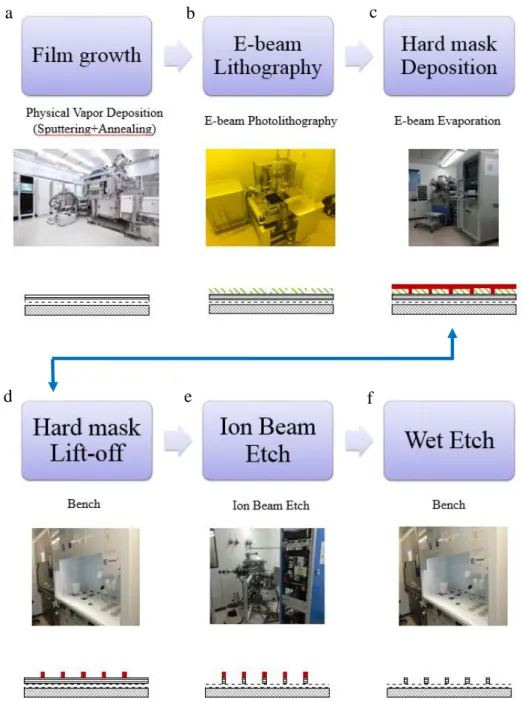
Figure 9 shows the full fabrication process flow of magnetic nanodots that I have developed during my PhD research.
Figure 9 Process flow for the fabrication of magnetic nanodots
a b c
22
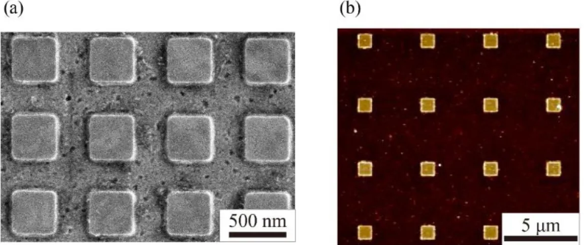
Nanodots with sizes ranging from 400 nm to 1 µm are fabricated using a lift-off process based on an Al hard mask. First, after spin coating the PMMA950A4 resist with a thickness of 200 nm, electron beam lithography (EBL) with 80 keV electrons is used to define the squared dots (step b). Subsequently, a 50-nm-thick Al mask is deposited by electron beam evaporation (step c). The resist is removed in 1165 solvent (step d) and then an ion milling process with Ar ions (etching angle of 45°) is used to etch the magnetic layers down to the CuN buffer layer using a secondary ion mass spectroscopy (SIMS) for the end point detection (step e). The final process is the removal of the Al mask by a wet etch process using a specific MF-CD-26 developer (step f). Figure 10 shows the typical high quality nanodots with vertical edges fabricated by this process.
Figure 10 The profile of a nanodot array. (a) SEM image of 400 nm nanodots (b) AFM image of 1 µm nanodots
2.2 Process flow for MTJ nanopillars
2.2.1 Growth of CoFeB-MgO based magnetic tunnel junction
The magnetic multilayers are deposited onto SiO2-coated Si wafers using a
combination of radio frequency (RF) and direct current (DC) sputtering in a Canon-Anelva system. From the substrate side, the MTJ structure consists of the following layers (the numbers are the nominal thicknesses in nanometers):
Ta(5)/Ru(15)/Ta(5)/Ru(15)/Ta(5)/Ru(5)/PtMn(20)/CoFeB(1.5)/CoFe(2.0)/Ru(0.85)/C oFeB(1.5)/CoFe(1.5)/MgO(0.8)/CoFe(1.5)/CoFeB(1.5)/Ru(2)/Ta(5)/Ru(10)
23
The bottom and top layers, Ta(5 nm)/Ru(15 nm)/Ta(5 nm)/Ru(15 nm)/Ta(5 nm)/Ru(5 nm) and Ru(2 nm)/Ta(5 nm)/Ru(10 nm), respectively, are designed for the Current-in-plane tunneling (CIPT) measurements using a CAPRES microprobe tool. The typical TMR ratio and the RA product of the unpatterned films are ~ 144% and =19 ohm·μm2, respectively. An annealing process is performed at 350°C for 1 hour with an in-plane magnetic field of 1 T under a vacuum of 10-6 Torr.
After the annealing, the magnetization curves are measured by VSM at room temperature. The free layer (CoFe(1.5 nm)/CoFeB(1.5 nm)), reference layer (CoFeB(1.5 nm)/CoFe(1.5 nm)) and pinned layer (CoFeB(1.5 nm)/CoFe(2.0 nm)) can be observed from the hysteresis loop under in-plane magnetic fields, as shown in Figure 11.
Figure 11 (a) In-plane magnetization hysteresis loops of the MTJ stack. The magnetic configuration of the free (F), reference (R) and pinned (P) layers are indicated by arrows. (b) Minor loop corresponding to the switching of the free layer.
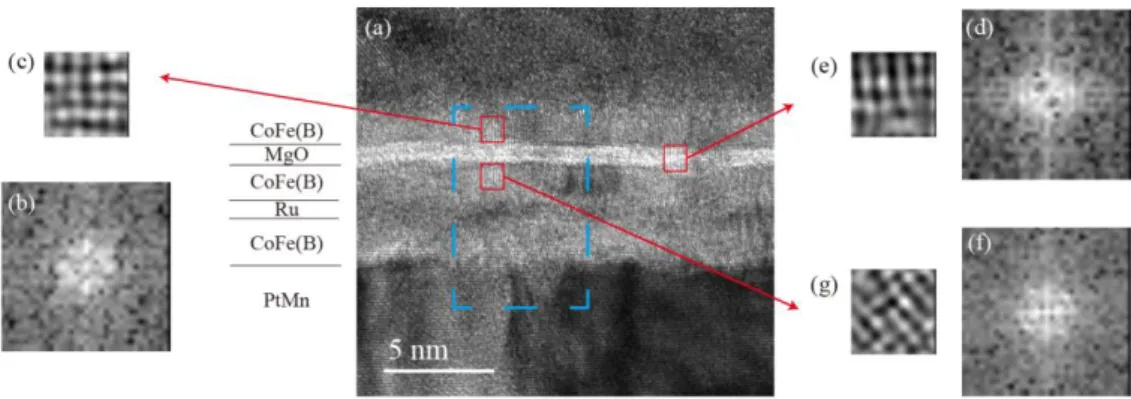
The presence of a good crystalline structure of the CoFe(B) and MgO layers, e.g. body-centered cubic (bcc) (001) and NaCl-structure respectively, is crucial for obtaining a high TMR ratio [YUA07]. As shown in Figure 12, the cross-sectional high resolution transmission electron microscopy (HRTEM) have been performed to characterize the lattice structure of the MTJ stack. The free layer (CoFe(B)), tunnel barrier (MgO), synthetic ferri-magnetic (SyF) reference layer (CoFe(B)/Ru/CoFe(B)) and anti-ferromagnetic layer PtMn are indicated. A crystalline structure can be observed for both CoFe(B) and MgO layers.
24
Figure 12 Cross-sectional TEM of magnetic multilayers in CoFe(B)-MgO based MTJ
In order to further investigate the crystalline structure for both CoFe(B) and MgO layers, fast Fourier transformation (FFT) have been performed for diffraction patterns, as shown in Figure 13. Four diffraction points in the top CoFe(B) layer can be observed in FFT diffraction images (see Figure 13 (b)), indicating a bcc structure of CoFe(B) [NAG06]. However, different lattice directions are also observed in the bottom CoFe(B) layer (see Figure 13 (f)) and MgO layers (see Figure 13 (d)). These twisted crystalline structures are possibly induced during the preparation process of TEM samples.
Figure 13 The crystalline structure analysis of the MgO and CoFe(B) layers of MTJ. The region in Figure 12 is marked by a blue dash rectangle. The original image (a) were firstly processed by a Gaussian filter (not showed), and then the fast Fourier transformation diffraction patterns (b, d, f) were obtained and finally, the crystalline lattice patterns (c, e, g) after the inversed FFT.
25
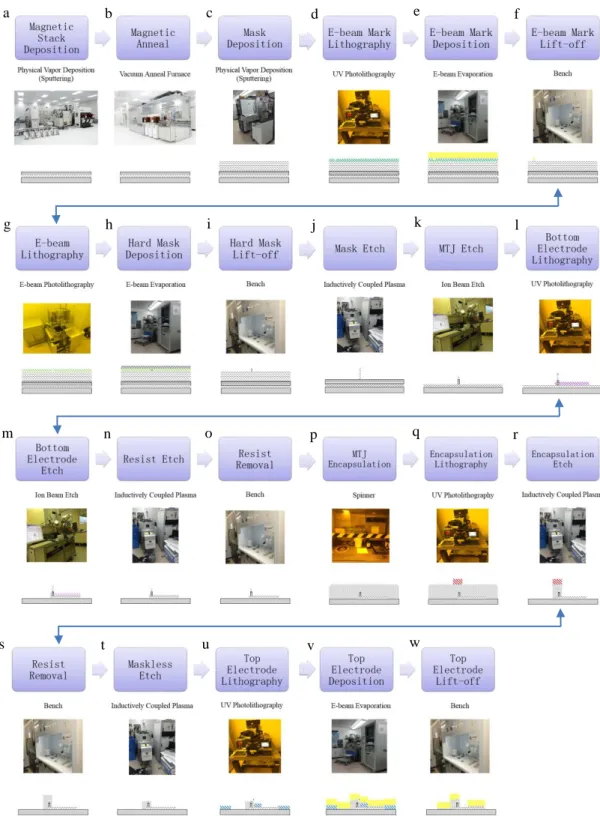
2.2.2 Nanofabrication process of MTJ nanopillars
The MTJ fabrication process can be divided into three different parts: MTJ lithography, MTJ etching and MTJ encapsulation. The typical process including these three important parts is described as following: submicron-sized ellipses are obtained using EBL process with a ZEP520A positive resist on top of a 150 nm Ta layer, followed by Pt evaporation and a lift-off process. Then the Pt patterns are used as a protective mask to etch down the 150 nm Ta layer using inductively coupled plasma (ICP). After that, the Ta patterns are used as a hard mask to etch down the magnetic multilayers using an optimized ion beam etching (IBE) process to avoid sidewall redisposition. A VM652 promoter and an Accuflo T-25 Spin-on Polymer (produced by Honeywell [HUA11]) are then sequentially spin coated, followed by a low-temperature curing process (below 300°C) for encapsulating the patterned structure in the SiOx-based materials. The encapsulation layer is patterned into 40×60 µm2
elements using ICP. Finally, Cr/Au top electrodes are fabricated utilizing a lift-off approach. The schematic of the final device is shown in Figure 14.
Figure 14 Schematic of the final MTJ device
Below, we give more details of the description in each step and the issues we have faced to develop this full process. All the process steps of the MTJ nanopillars are listed below:
26
1. A Ta layer with a thickness of 80 nm is deposited by sputtering onto the top of magnetic multilayers as a hard mask. (step c)
2. Alignment marks for the EBL process are realized. Here, a lift-off process is involved, including optical lithography with positive photoresist AZ5214, metal e-beam evaporation of Ti/Au and lift-off with Acetone. (step d-f)
3. Once the EBL alignment marks are done, a second lift-off process is involved, including EBL of 80 keV electrons with positive e-beam resist ZEP520A of a thickness of 400 nm, metal Pt e-beam evaporation with a thickness of 80 nm and lift-off with a Butanone. After those steps, the pattern (the shape of nanopillar) has been transferred to the hard Pt mask. (step g-i)
4. ICP dry etching with a mixture of SF6 and Ar is used to etch the Ta mask using the
hard Pt mask. In this step, the pattern (the shape of nanopillar) is transferred to the Ta mask. (step j)
5. IBE dry etching with 45º is used to etch the magnetic multilayers using the Ta mask. The etching stops at the seed layer of the MTJ stack (e.g. Ta/Ru/Ta). In this step, the pattern (the shape of nanopillar) is transferred to the magnetic multilayers. (step k) 6. Definition of the pattern of the bottom electrode, including the optical lithography with AZ5214 resist and the following IBE dry etching with 45º. The etching stops in the SiO2 substrate. (step l-m)
7. Resist removal, including an ICP dry etch with O2 and a wet etch with 1165 solvent.
After this step, the MTJ nanopillar will be exposed to O2. (step n-o)
8. MTJ encapsulation, including spin-coating VM652/Accuflo and low-temperature curing process below 300 ºC. (step p)
9. Definition of the pattern for the encapsulation layer, including the optical lithography with AZ5214 resist and the following ICP dry etch with a mixture of O2
and Ar. Then the resist is removed by wet etching in Acetone. (step q-s)
10. Fabrication of the top contact. First, the top Ta mask is opened by etching the encapsulation layer with ICP dry etch with a mixture of O2 and Ar (step t). Then the
27
lithography with positive photoresist with AZ5214 resist, metal e-beam evaporation of Ti/Au and lift-off with Acetone. (step v-w)
Figure 15 gives the fabrication flow of the MTJ nanopillar as described above.
Figure 15 Process flow for the fabrication of MTJ nanopillar
2.2.2.1 MTJ lithography
Five levels of lithography are needed for the full process: one level for the EBL
a b c d e f
g h i j k l
m n o p q r
28
process and four levels of optical lithography for the alignment marks, bottom/top electrodes and encapsulation layer. The layouts, e.g. photomasks, for the optical lithography are showed in Figure 16.
Figure 16 Layout of the photomasks for MTJs
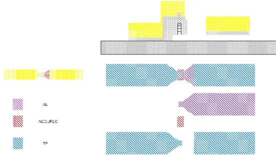
The photomasks are designed for 4-inch wafer but they are also compatible with 1cm×1cm or 2cm×2cm samples. The details for the shape and relative location of the three-level (e.g. bottom electrode, top electrode and encapsulation layer) photomask layouts are presented in Figure 17. The MTJ nanopillar is located at the narrow constriction of the bottom electrode and it is encapsulated with the Accuflo.
Figure 17 Layout of a single MTJ cell. “BE” represents the “Bottom Electrode”, “TE” represents the “Top Electrode” and “ACCUFLO” represents the encapsulation layer.
29
Figure 18 shows the top view of a fabricated MTJ device under SEM. The bottom electrode, top electrode, MTJ nanopillar and encapsulation layer are indicated.
Figure 18 Top view of MTJ device under SEM. The red dash circle marks the location of a MTJ nanopillar and the inset image shows the nanopillar under a tilt view of 45 degree.
2.2.2.2 MTJ etch
The etching of MTJ is the most difficult and crucial step, which directly determines the profile and performance of the device. In this section, several important points are highlighted and discussed.
① Use of IBE to etch the MTJ
Since the FM layer, e.g. CoFeB, is very sensitive to the oxygen and halogen elements (F and C based compounds), the IBE method is more suitable than ICP for etching the core structure of the MTJ stack, e.g. CoFe(B)/MgO/CoFe(B).
② The use of a hard Ta mask for the IBE process
Since a vertical current has to flow through the nanopillar and an e-beam resist mask is very difficult to remove after IBE, we have developed a process based on a Ta mask, for which the etching rate is quite low in the milling process.
③ Use of a hard Pt mask to etch the Ta layer
As discussed above, a Ta mask is needed to etch the nanopillar. Furthermore, in order to pattern the Ta layer with the shape of nanopillar, an additional metallic hard mask is
30
needed. For that, a lift-off process is used involving the EBL with positive resist followed by the deposition of a metallic layer as hard mask. There is a trade-off in the resist thickness: the metallic hard mask should be sufficient thick for the etching process, however, the e-beam resist should be sufficient thin for a better EBL resolution. The best compromise we have found is to use a positive e-beam resist with high resolution (ZEP520A). Due to the high etching selectivity ratio, Pt has been chosen as the hard mask for etching the Ta using ICP.
④ Use of SF6 and Ar to etch the Pt layer using a ICP process
For ICP, there are two etching processes involved. The first one is physical etching, based on Ar ions. The second process is chemical etching, which originates from the chemical interaction between a reactive gas of ions and the layer to be etched. A failure for using the improper parameters (pressure, gas flow rate, acceleration voltage …) will lead to a low etch selectivity and a bad device profile. In other words, a right combination of physical and chemical etching is expected.
In order to improve the ICP process, up to 8 different recipes have been tested on more than 10 samples. The SEM image of the etched MTJ nanopillar under the best recipe (the etching duration is 46 minutes) has been shown in Figure 19 (a) and a very good vertical profile has been achieved. A clear interface between the Pt and Ta masks can be observed in Figure 19 (b) for larger patterns as dummy (used for checking the patterns).
Figure 19 A good profile of the metallic hard mask (Pt and Ta) nanopillar is shown in (a). A clear interface of Pt and Ta layers is shown in (b) for larger patterns.
31
It needs to be noted that the etching process described above is discontinuous in the sense that we have used 6 periods of etching with idle time in between. If we do a continuous etching for the same duration (e.g. 46 minutes), a ring appears at the bottom of the nanopillar (see Figure 20), which can be due to an over physical etching.
Figure 20 SEM image of the metallic hard mask (Pt and Ta) nanopillar after a continuous ICP process (e.g. 46 minutes).
We have found that a heating process involved in the physical etching can explain this result. By lowering down the etching power, a very goodmetallic hard mask (Pt and Ta) profile and a very good etching selectivity (between Pt and Ta) can be obtained again, as shown in Figure 21.
Figure 21 SEM image of the metallic hard mask (Pt and Ta) nanopillar after ICP etching
⑤ IBE etching of the MTJ stack using the Ta mask
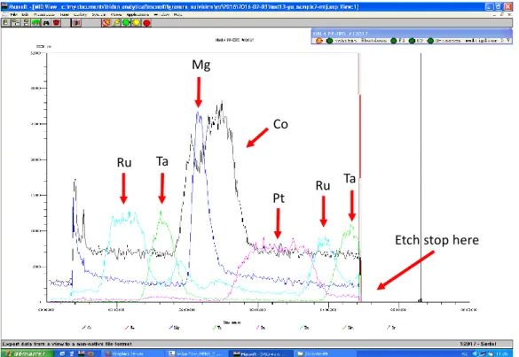
As we have mentioned at the beginning of this section, we use IBE to etch the MTJ stack. The screenshot of the SIMS measurement for the end-point detection (see Figure 22) indicates that the etching stops at the top Ta layer of the bottom electrode.
32
Figure 22 SIMS measurement for the IBE process of the MTJ stack
The IBE process is done at 45° to minimize the redeposition on the sidewall of the MTJ nanopillar [SUG09, PRE15], as shown in Figure 23.
Figure 23 Schematic drawing of the IBE process used here. The figure is reproduced from Sugiura et al. [SUG09]
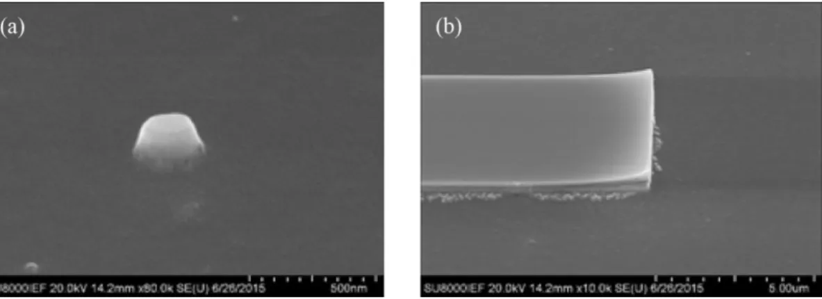
The SEM images of the MTJ nanopillars with 15° and 45° IBE angles are presented in Figure 24 (a) and (b), respectively. A clear tail at the bottom of the nanopillar is shown only for 45° (see Figure 24 (b)), which is due to the shadow effect in IBE [SUG09]. Decreasing the etching angle to 15° helps to reduce the tail, as shown in Figure 24 (a);
Mg Ta Ta Ru Ru Pt Co
33
however, the later transport measurement for the fabricated MTJ devices shows an electrical short-cut, which indicates a redeposition on the sidewall [PEN09]. We note that the existence of redeposition can be further confirmed by the TEM check with very high resolution on the sidewall of MTJ [PEN09]. Although a multi-step etch strategy could be utilized to eliminate the tails [CHU12], we used 45° as the etching angle in IBE.
Figure 24 SEM image of the MTJ nanopillar after IBE with different etch angles. The etch angle for (a) and (b) are 15° and 45° respectively.
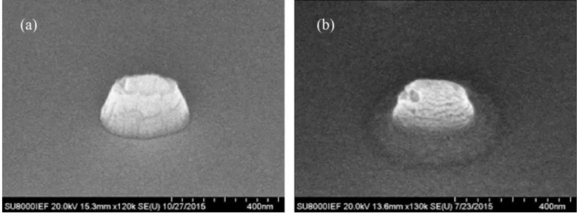
Figure 25 shows a MTJ nanopillar after IBE with an etch angle of 45°. The size of the nanopillar is around 100 nm and the sidewall is vertical. The cylinder on the top is the left Ta mask and the circular shape below is the MTJ stack. The dimension of the tail here is around 400 nm, which indicates the limitation for high density nanopillars using IBE techniques [PRE15].
34
2.2.2.3 MTJ encapsulation
In order to protect the nanopillars from oxidation, to insure electrical insulation and to maintain the mechanical stiffness of the nanopillars, an encapsulation matrix is necessary. In the semiconductor industry, SiO2 and SiN are widely used as
encapsulation material due to their good electrical insulation and thermal stability. Both sputtering and plasma enhanced chemical vapor deposition (PECVD) can be used for depositing such materials, however, either an etch-back process or a chemical mechanical polishing (CMP) process is needed for the later step of electrodes contact.
Another possible solution is the utilization of a spin-on glass. As a method of planarization, the use of spin-on glass gets rid of the extra step of dry etching or CMP process. Due to the liquid feature of spin-on glass, it can be spun off on the sample surface and then turns into SiO-based material using a curing process. Figure 26 shows the results of electron energy loss spectroscopy (EELS) mapping for the spin-on polymer Accuflo provided by the Hspin-oneywell Company that we have used in our process. The exact details of molecular formula is unknown, however, the carbon, oxygen and silicon elements are detected from the EELS measurement.
Figure 26 Element analysis of the spin-on polymer Accuflo. The region for EELS testing is marked by a green rectangle in STEM image obtained by a high-angle annular dark field (HAADF) detector. The EELS mapping indicates the existence of carbon, oxygen and silicon elements in Accuflo.
35
For the MTJ encapsulation, it is important to use a curing temperature below 300°C to avoid any further annealing of the magnetic multilayers, which may lead to a degradation of the TMR ratio [PRE15, LEE07, IKE08, JAN11]. It is also necessary to pattern the encapsulation layer into micro-sized rectangle. The purpose for the patterning is to minimize the effect of capacitance. As shown in Figure 14, metal-insulator-metal (MIM) structure including the top electrode, the bottom electrode and the encapsulation layer in between, is similar to a plate capacitance. By decreasing the area of the encapsulation layer, the capacitance can be reduced. Figure 27 shows the patterned encapsulation layer. A small dot well encapsulated in the Accuflo can be observed at the extremity of the bottom electrode, which is actually the MTJ nanopillar (see Figure 27 (a)).
Figure 27 Images of the encapsulation layer after patterning under (a) optical microscope and (b) SEM .The dash circle marks the location of the nanopillar.
After the patterning process, the thickness of the encapsulation layer needs to be reduced by ICP dry etch down to the top of the Ta mask, as shown in Figure 28. Figure 28 (b) shows clearly that the top of the Ta mask has been opened and is ready for the later step of depositing the Au electrode.
36
Figure 28 SEM images of the (a) square of dummy (used for checking the patterns) and (b) the top of Ta nanopillar after the process of etching down the encapsulation layer by ICP.
Finally, the cross-sectional TEM images of the fabricated MTJ devices with the top electrode are presented in the Figure 29.
Figure 29 Cross-sectional TEM images of the MTJ nanopillar with a size of 80nm×200nm
2.3 Summary
In this section, we have discussed about the nanofabrication process flow of two magnetic devices, e.g. magnetic nanodots down to 400 nm and MTJ nanopillars down to 100 nm. For the magnetic nanodots, a process based on IBE through an Al mask followed by a wet etch of the mask has been developed. For MTJ nanopillar, we have shown that crucial steps include the optimization of the etching process using both ICP and IBE with Ta and Pt hard masks, as well as the encapsulation process with a
37
low-temperature curing for encapsulation layer Accuflo and an ICP process to open the top contact. In the next two chapters, we are going to study the switching process in these devices, i.e, field-induced switching in nanodots with PMA and current-induced switching in the MTJ nanopillars with in-plane magnetization.
38
CHAPTER 3 MAGNETIZATION REVERSAL OF
NANODOTS GOVERNED BY LAPLACE PRESSURE
In this chapter, we study the magnetization reversal of CoFeB-MgO nanodots with perpendicular anisotropy under magnetic field for sizes ranging from w=400 nm to 1 μm. We show that contrary to previous experiments for patterned media, the switching field distribution (SFD) is shifted toward lower magnetic fields as the size of the elements is reduced with a mean switching field varying as 1/w. We demonstrate that this mechanism can be explained by the nucleation of a magnetic domain wall (DW) at the edges of the nanodots where damages are introduced by the patterning process followed by a DW depinning process.
3.1 Magnetic reversal mechanism
Magnetic nanostructures based on PMA [HEL17] materials are attracting a large amount of attention for their potential applications including high-density MRAM [IKE10, KEN15], bit patterned media [OCON10, ALB15], or magnetic logic [TOR17]. The scalability of these applications toward ultimate technology nodes is in general limited by the structural variability of the nanostructures. This leads to a dispersion of the magnetic properties, which strongly affects the switching mechanism when the dimension of the nanostructures becomes smaller. In particular, this has been extensively shown for the switching process of magnetic dots [HUG05, THO06, SHA08, OKA12, SUT16]. When the size of the dots is sufficiently large, the dominant mechanism for switching has been found to be nucleation followed by rapid propagation of domain walls (DWs). In this case, as the propagation fields are usually lower than the nucleation fields [HUG05, BUR13], the SFD corresponds to the distribution of nucleation fields, which is related to the distribution of magnetic anisotropy in the films. As the size of the dot decreases, the SFD is enlarged and shifted toward higher fields. A simple model taking into account the initial intrinsic distribution of magnetic anisotropy in the films can explained these results [HUG05, THO06]. When the dots become mono-domains (typically for sizes < 30 nm), a
39
coherent reversal described by the Stoner–Wohlfarth model is expected [STO48]. However, due to the distribution of magnetic anisotropy in the films, the SFD is also increased when the dot size is reduced. In addition to such variability of magnetic properties in the pristine films, edge damages introduced by the patterning process can also have a strong influence on the switching behavior. This is the case for instance for STT-MRAM or DW-based nanodevices where the edges have been found to reduce the efficiency of the switching process at small dimensions [CAY04, KIN14, NOW16].
3.2 Kerr microscopy
In this section, we first introduce the concept of magneto-optical Kerr effect and then describe the Kerr microscopy setup that has been used in the invesitagation of field-induced switching of magnetic nanodots.
3.2.1 Magneto-optical Kerr effect
In order to directly observe the reversal process of magnetic nanodots, a Kerr microscope has been utilized. The Kerr microscope is based on the magneto-optic Kerr effect (MOKE) which was discovered in 1877 by John Kerr [Ker58]. When a beam of light passes through a polarizer, it will be polarized; and when a beam of polarized light is reflected from the surface of magnetic film, the direction of polarization of the light will rotate by an angle. This phenomenon is called the MOKE effect, as shown in Figure 30.