A 512kb 8T SRAM macro operating down to 0.57V
with an AC-coupled sense amplifier and embedded
data-retention-voltage sensor in 45nm SOI CMOS
The MIT Faculty has made this article openly available.
Please share
how this access benefits you. Your story matters.
Citation
Qazi, M. et al. “A 512kb 8T SRAM Macro Operating down to 0.57V
with an AC-coupled Sense Amplifier and Embedded
Data-retention-voltage Sensor in 45nm SOI CMOS.” Solid-State Circuits Conference
Digest of Technical Papers (ISSCC), 2010 IEEE International. 2010.
350-351. Copyright © 2010, IEEE
As Published
http://dx.doi.org/10.1109/ISSCC.2010.5433818
Publisher
Institute of Electrical and Electronics Engineers
Version
Final published version
Citable link
http://hdl.handle.net/1721.1/62194
Terms of Use
Article is made available in accordance with the publisher's
policy and may be subject to US copyright law. Please refer to the
publisher's site for terms of use.
350
• 2010 IEEE International Solid-State Circuits Conference
ISSCC 2010 / SESSION 19 / HIGH-PERFORMANCE EMBEDDED MEMORY / 19.5
19.5
A 512kb 8T SRAM Macro Operating Down to 0.57V
with An AC-Coupled Sense Amplifier and Embedded
Data-Retention-Voltage Sensor in 45nm SOI CMOS
Masood Qazi1, Kevin Stawiasz2, Leland Chang2, Anantha Chandrakasan1 1Massachusetts Institute of Technology, Cambridge, MA
2IBM T. J. Watson, Yorktown Heights, NY
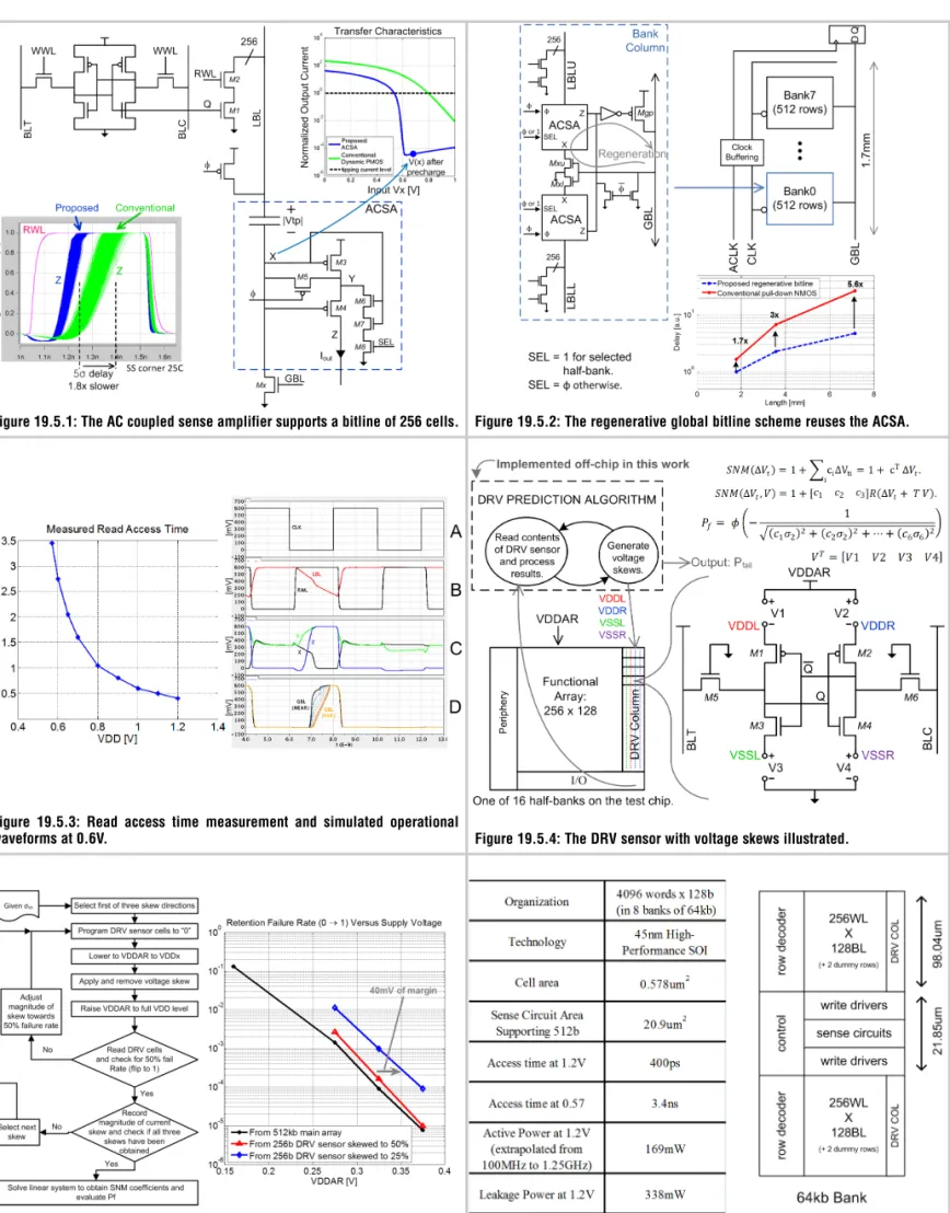
There is a need for large embedded memory that operates over a wide range of supply voltage compatible with the limits of static CMOS logic that also mini-mizes standby power [1,2]. A 512kb 8T SRAM macro in 45nm SOI CMOS is developed as a building block for this application. It addresses the design chal-lenges related to area efficiency and process variation with three contributions: 1) an AC coupled sense amplifier (ACSA) that operates at a power supply ulti-mately limited by the worst-case bit line on/off current ratio; 2) area efficient, regenerative driving of long data lines to permit bidirectional signaling on a sin-gle metal 4 wiring track on the memory cell column pitch; 3) a data retention voltage (DRV) sensor to determine the mismatch-limited minimum standby sup-ply voltage without corrupting the contents of the memory.
The ACSA is shown in Fig. 19.5.1. During precharge (φ=0), device M5 diode-connects the sensing PMOS M3, charging the input capacitor to the VTof M3.
Loading from devices M6-M8 and stacking from M4 establishes a steep trans-fer characteristic near the tipping current level at the dynamic output Z. A thick oxide MOS capacitor achieves a coupling ratio close to 1 while keeping the area of the entire ACSA under 9µm2. During sensing (φ=1, RWL=1), node X is
initial-ized 50mV above the tipping point of the ACSA through Cgdcoupling and charge
injection from M5. When reading a 1, devices M2 and M1 discharge the local bit-line, and after 100mV of signal development the output current quickly charges node Z to VDD. Waveform plots B and C in Fig. 19.5.3 show amplification when reading 1 and stability when reading 0.
The conventional domino read path [3], which replaces the ACSA by an optimal-ly sized PMOS device of the same VT, is 1.8x slower (Fig. 19.5.1). Monte Carlo
simulation of the 5σ timing window reveals that additional variation of the dynamic PMOS also restricts the minimum operating VDD to 0.9V; whereas, the ACSA works down to 0.53V (FF corner, 85C). Small-signal, single-ended sens-ing with offset compensation has also been employed in [5] and [6]. By AC cou-pling, this work avoids the unconditional full VTswing on the bitlines and the
requirement for interlock between wordline access and precharge found in [6]. By exploiting the sharp cutoff characteristics of a PMOS stack M3-M4 to sepa-rate 1 from 0, this work avoids the 2 capacitors, 13 transistors, and power penal-ty related to regenerative feedback in [5]. Hence, 128 parallel ACSAs can be laid out on the bitline pitch, satisfying the non-interleaved column constraint of low-voltage 8T SRAM to avoid half-selected write operation.
After local sensing, data is forwarded across eight 64kb banks in the read cycle via the regenerative global bitline scheme (RGBS) shown in Fig. 19.5.2. Two ACSAs with shorted outputs are buffered to the global pull-up PMOS Mgp. When accessing bank0, device Mgp needs only to charge up the GBL input to the neighbor bank1 above the VTof NMOS Mxu/Mxl to trigger the next ACSA,
turn-ing on device Mgp in bank1 and so on until the data traverses the 1.7mm glob-al bitline (plot D Fig. 19.5.3). The simulated delay of the RGBS is 40% faster than the conventional pull down NMOS. The RGBS scales linearly with distance, pre-serving sharp transitions and performance comparable to a buffering daisy chain [7]; yet the RGBS avoids cross-over currents and enables bidirectional signal-ing—preventing routing congestion of the 128b word—through a single metal 4 track on the memory cell pitch.
The access times in Fig. 19.5.3 equal the minimum difference between the falling edge of CLK and the rising edge of ACLK (Fig. 19.5.2). Each measurement cor-responds to 100% pass of all 512kb under alternating checkerboard and blanket data patterns. Two measurements below 0.65V require partial turn-on of a bleed-er PMOS device on the bitlines to compensate for fast process cornbleed-er leakage. Performance scales from 400ps at 1.2V to 3.4ns at 0.57V. Measured leakage power scales down 9.4x over this range. The read path benefits from CMOS scal-ing by avoidscal-ing differential sense amplifiers, which are sensitive to mismatch, and variable timing control signals [4,5].
For idle banks, lowering the supply to the DRV—measured to lie between 0.375V and 0.4V—reduces leakage power by 29x going from 1.2V to 0.4V. Generally the minimum supply voltage is determined by the one memory cell out of 524,288 with the largest DRV, resulting from local mismatch variation and its functional relation to the static noise margin (SNM) of the memory cells. This
relation changes with process corner, temperature, and end-of-life degradation. Prior work [8,9] recognizes the importance of tracking the DRV but relies on apriori characterization of the main memory. The primary challenge remains: how to determine the DRV without corrupting the contents of the main memory?
In this work, a separate column of 256 cells is employed in conjunction with sta-tistical techniques as a DRV sensor to predict the 5σ failure rate of the main memory (Fig. 19.5.4). The test chip contains 4096 DRV sensor cells but only one segment of 256 is measured to demonstrate the area efficiency of the technique. The layout of DRV sensor cells is identical to the main memory cells except for one modification: the metal 2 wire supplying VDDAR is split into two separate VDDL and VDDR supply lines. Along with VSSL and VSSR, the four independent supplies of the DRV sensor cells are used to program and skew without access-ing the main memory.
Given a 1σ measurement of VTvariation in memory cell devices, the DRV
sen-sor is skewed in multiple directions to reconstruct the SNM as a linear function of VT. The resulting coefficients are combined with σVtto estimate failure. The
detailed algorithm in Fig. 19.5.5 searches the magnitude of three linearly inde-pendent voltage skews that collapse the nominal SNM, as observed by 50% fail-ure in the 256 memory cells. The application of voltage skews emulates an effec-tive shift in threshold voltage—through a transformation represented by T in the matrix equation of Fig. 19.5.4—since the drain current depends on (VGS– VT)
and the voltage skews directly add to or detract from VGS. By simplifying
coeffi-cients (assuming M5 and M6 do not influence retention and M3 and M2 have similar influence on the SNM), a system of three equations and three unknowns can be solved. The measurement results in Fig. 19.5.5 show that the predicted retention failure matches the actual retention failure in the main memory. A con-servative estimate is also produced by replacing the failure criterion of 50% with 25% in the prediction algorithm, introducing a measured margin of 40mV. Thus, for real-time embedded operation, the DRV sensor can permit aggressive reduc-tion of retenreduc-tion standby voltage with negligible risk of losing data. This tech-nique is relevant to state-of-the-art embedded SRAM that requires the retention voltage as an input to standby power regulation circuits [10].
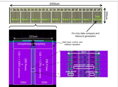
Figure 19.5.6 lists key features of the fabricated 8T SRAM, a viable candidate for voltage scalable operation down to 0.57V. The die photo in Fig. 19.5.7 illustrates the 2.0mm x 0.35mm chip floor plan containing 8 banks of 64kb along with on-chip testability circuits.
Acknowledgements:
This work was funded in part by the FCRP Focus Center for Circuit & System Solutions (C2S2), under contract 2003-CT-888. The authors thank Robert Montoye for technical discussion and Keith Jenkins for test support. References:
[1] D. J. Frank, W. Haensch, G. Shahidi, O. Dokumaci, “Optimizing CMOS Technology for Maximum Performance,” IBM J. Res. Dev., vol. 50, pp. 419, Jul., 2006.
[2] R. Krishnamurthy, et al., “High-performance, Low-power, and Leakage-toler-ance Challenges for Sub-70nm Microprocessor Circuits,” ESSCIRC Dig. Tech. Papers, pp. 315-322, Sept., 2002.
[3] L. Chang, et al., “A 5.3GHz 8T-SRAM with Operation Down to 0.41V in 65nm CMOS,”Dig. Symp. VLSI Circuits, pp. 252-253, Jun., 2007.
[4] K. Zhang, et al., “The Scaling of Data Sensing Schemes for High Speed Cache Design in Sub-0.18µm Technologies,”Dig. Symp. VLSI Circuits, pp. 226-227, Jun., 2000.
[5] N. Verma and A. P. Chandrakasan, “A High-Density 45nm SRAM Using Small-Signal Non-Strobed Regenerative Sensing,” ISSCC Dig. Tech. Papers, pp. 380-381, Feb., 2008.
[6] I. Arsovski and R. Wistort, “Self-referenced Sense Amplifier for Across-chip-variation Immune Sensing in High-performance Content-Addressable Memories,” CICC Dig. Tech. Papers, pp. 453-456, Sept., 2006.
[7] K. Zhang, et al., “A Fully Synchronized, Pipelined, and Re-Configurable 50Mb SRAM on 90nm CMOS Technology for Logic Application,” Dig. Symp. VLSI Circuits, pp. 253-254, Jun., 2003.
[8] J. Wang and B. Calhoun, “Canary Replica Feedback for Near-DRV Standby VDDScaling in a 90nm SRAM,” CICC Dig. Tech. Papers, pp. 29-32, Sept., 2007.
[9] H. Qin, Y. Cao, D. Markovic, A. Vladimirescu and J. Rabaey, “SRAM Leakage Suppression by Minimizing Standby Supply Voltage,” ISQED Dig. Tech. Papers, pp. 55-60, Mar., 2004.
[10] Y. Wang, et al., “A 4.0 GHz 291Mb Voltage-Scalable SRAM Design in 32nm High-k Metal-Gate CMOS with Integrated Power Management,” ISSCC Dig. Tech. Papers, pp. 456-457, Feb., 2008.
351
DIGEST OF TECHNICAL PAPERS •
ISSCC 2010 / February 10, 2010 / 10:45 AM
Figure 19.5.1: The AC coupled sense amplifier supports a bitline of 256 cells. Figure 19.5.2: The regenerative global bitline scheme reuses the ACSA.
Figure 19.5.3: Read access time measurement and simulated operational waveforms at 0.6V.
Figure 19.5.5: DRV Sensor algorithm and measurement results from test chip. Figure 19.5.6: Summary of chip characteristics and 64kb bank floor plan. Figure 19.5.4: The DRV sensor with voltage skews illustrated.
• 2010 IEEE International Solid-State Circuits Conference
978-1-4244-6034-2/10/$26.00 ©2010 IEEE
ISSCC 2010 PAPER CONTINUATIONS
Figure 19.5.7: Die photo of the 512kb SRAM test chip in 45nm SOI CMOS along with a close-up snapshot of the bank layout. Global bit lines run 1.7mm long from left to right across 8 banks of 64kb each.