HAL Id: hal-01745071
https://hal.archives-ouvertes.fr/hal-01745071
Submitted on 18 Apr 2018
HAL is a multi-disciplinary open access
archive for the deposit and dissemination of
sci-entific research documents, whether they are
pub-lished or not. The documents may come from
teaching and research institutions in France or
abroad, or from public or private research centers.
L’archive ouverte pluridisciplinaire HAL, est
destinée au dépôt et à la diffusion de documents
scientifiques de niveau recherche, publiés ou non,
émanant des établissements d’enseignement et de
recherche français ou étrangers, des laboratoires
publics ou privés.
polytypes in the SiC (CVI) matrix of SiC/SiC
composites
Sylvie Schamm-Chardon, Annie Mazel, Dominique Dorignac, Jean Sévely
To cite this version:
Sylvie Schamm-Chardon, Annie Mazel, Dominique Dorignac, Jean Sévely.
HREM
identifi-cation of ”one-dimensionally-disordered” polytypes in the SiC (CVI) matrix of SiC/SiC
com-posites.
Microscopy Microanalysis Microstructures, EDP Sciences, 1991, 2 (1), pp.59-73.
�10.1051/mmm:019910020105900�. �hal-01745071�
HREM
identification
of
"one-dimensionally-disordered"
polytypes
in the
SiC
(CVI)
matrix of
SiC/SiC
composites
Sylvie
Schamm,
AnnieMazel,
Dominique
Dorignac
and JeanSévely
CEMES-LOE/CNRS,
B.P.4347, 31055
ToulouseCedex,
France(Received
October18, 1990,
accepted
December17, 1990)
Résumé. 2014 La matrice de carbure de silicium des
composites
SiC/SiC a été examinée d’unpoint
devue
chimique
et structural parspectroscopie
de pertesd’énergie
d’électrons(EELS)
et parmicrosco-pie électronique à
haute résolution(MEHR).
La croissance colonnaire des cristaux de la matrice etleur distribution radiale par rapport aux fibres
qui
constituent le renfort sontcaractéristiques
de cematériau. La st0153chiométrie des cristaux a été vérifiée
(Si/C
=1).
La structurecubique (polytype 3C)
de certains d’entre-eux a été identifiée à l’aide des
diagrammes
de diffraction. Dans le cas d’autrescris-taux, dits
"polytypes
de désordreunidimensionnel",
l’imagerie
haute résolution s’est avérée nécessairepour mettre en évidence la
désorganisation
dans la directiond’empilement
des couches de tétraèdres. La résolutionponctuelle,
0,19
nm, dumicroscope
PHILIPSCM30-ST,
fonctionnant à 300kV,
permetde reconnaître la structure
projetée
de SiC et d’évaluer ledegré
de désordre dans cespolytypes.
La si-mulationnumérique
desimages
nous apermis d’interpréter
sansambiguité
nos clichésexpérimentaux.
Abstract. 2014 The matrix of SiC/SiCcomposites
has been observedby
electron energy lossspec-troscopy
(EELS)
andhigh
resolution electronmicroscopy
(HREM)
from both the chemical and the structuralpoint
of view. In thismaterial,
columnargrowth
and radial arrangement around the fibres of the reinforcement aretypically
observed for thecrystal
of the matrix. Theratio,
Si/C
=1,
ofthese
crystals
has been checked. The cubic structure of some of them has been identifiedthrough
their diffractionpatterns.
High
resolutionexperiments
wereperformed
torecognize
the structure of the otherspolytypes,
which are characterizedby
a disorder in the direction of the tetrahedrallayer
stacking.
For this reason,they
arecalled,
"one-dimensionally-disordered" polytypes.
The PHILIPS CM30-STpoint
resolution(0.19 nm)
enables theprojected
SiC structure to berecognized
so that thedegree
of disorder in thispolytype
can be estimated. Theinterpretation
of theexperimental images
was based on
comparison
with simulations.Classification
Physics
Abstracts61.16D - 81.15H
1. Introduction.
The fact that a
composite
made of two brittle constituents(ceramics)
may not be brittlejustifies
the interestduring
recent years in ceramic matrixcomposites (CMC)
[1].
Tbughened
CMCconsisting
of a fibrouspreform
embedded in a ceramic matrix arebeing developed
as apotential
solutionto some of
today’s high
temperature
materials needs.Among
them areSiC/SiC
composites,
the matrix of which isinvestigated
in thispaper.
The
properties
of CMC aregoverned by
the characteristics of their différentconstituents,
Le. thefibre,
the matrix and also the interface between them. Therelationships
between theseprop-erties and characteristics are not
yet
clearly
understood. This could be remediedby characterizing
simultaneously
the microstructure of the constituents and the mechanicalproperties
of thecorre-sponding composite.
Numerous models havealready
beendeveloped
to describe the mechanical behaviour of theCMC,
but their microstructure has not beenthoroughly investigated.
By using
electron energy lossspectroscoy
(EELS)
andhigh
resolution electronmicroscopy
(HREM),
it ispossible
to characterize materials from the chemical and the structuralpoint
of view at aquasi-atomic
scale. Theapplication
of such studies to the différent constituents of the CMC is nownecessary
for theirdevelopment.
The reinforcement
(Nicalon
type
fibres)
and the interface in theSiC/SiC
composites
haveal-ready
been observed at nanometric resolution[2-5],
but the matrix has not hitherto been consid-ered. The latter is obtainedaccording
to the ChemicalVapour
Infiltrationprocess
(CVI).
In thisprocess,
theopen
porosity
of a fibrouspreform
is infiltratedby
reactant gases thatdecompose
atelevated
temperature
(about
1000° C)
todeposit
silicon carbide between and around the fibres[6].
The microstructure of theSiC(CVI)
isstrongly dependent
on the numerouspreparation
param-eters such as
temperature,
totalpressure,
gascomposition
and flow rate. Thisinvestigation
wasinitiated to characterize the microstructure of the SiC matrix and to determine which of the SiC structural forms
(polytypes)
have beendeposited during
the CVIprocess.
HREM wasperformed
with JEOL 200CX-S and PHILIPS CM30-ST
microscopes.
In order tointerpret
the contrast of theexperimental images correctly, they
have beencompared
with simulated ones which take intoaccount the various
parameters
involved in thehigh
resolutionexperiments (voltage,
defocus,
thickness and orientation of the
sample)
[7].
2.
Polytypism
of silicon carbide.The différent
polytypes
of silicon carbide(more
than 150 differentforms)
are all basedupon
aframework of
SiC4
(or
CSi4)
tetrahedral units. These units are associated withinlayers by
three of their vertices in the same way as hardspheres
in acompact
structure. 1Bvo succesivelayers
occupypositions
which are related to one another eitherby
asimple
translation(cubic polytype 3C)
orby
both a translation and a rotation of 1800(hexagonal
polytypes, e.g.
6H)
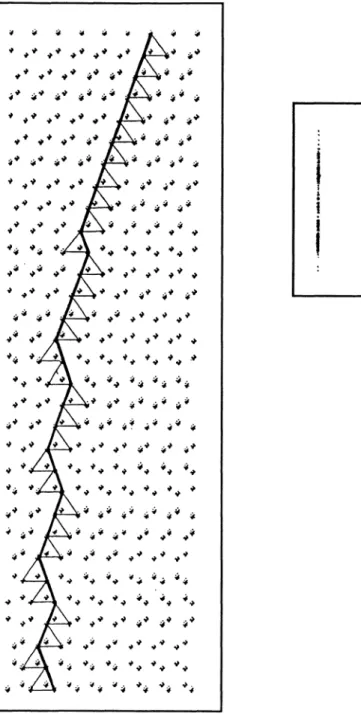
(Fig. 1). Polytypism
in silicon carbide results from theability
of the tetrahedral unitlayers
to be stackedaccording
to différent
sequences
on the basis of these two modes. All SiCpolytypes
have two structuralparameters
in common(that
of the tetrahedral basalplane),
a = 6 = 0.308 nm.They
differonly
by
the thirdparameter,
which is amultiple
of the tetrahedral unitheight (in
the direction of thestacking sequence),
i.e. c = 0.25 x N nm(Fig. 1).
N is theperiodicity
of thepolytype,
that is tosay the number of
layers
after which thestacking
recurs. Shortperiod
polytypes,
denoted2H, 4H,
6H, 15R
and 3C in the Ramsdell notation(H
forhexagonal,
R forrhombohedral,
C forcubic),
arecalled "basal structures" of SiC because
polytypes
oflarge
cparameter
can be constructed fromstacking
sequences
of thesepolytypes.
When SiC is observed
along
a 1120 >(hexagonal structures)
or 110 >(cubic structure)
direction,
it ispossible
to visualize thestacking
sequence
of thetetrahedral layers
[8-12].
With such an orientation and for ahigh enough
resolution of themicroscope,
the exact nature of eachpolytype
can be identified. Thepoint
resolutions of the JEOL 200CX-S and PHILIPS CM30-STmicroscopes
are 0.27 and 0.19 nm,respectively.
These values are sufficient to visualize theprojected
SiC bicolumnsseparated by
0.307 and 0.266 nm as shown infigure
1,
whichrepresents
the
projected
interatomic distances of the tetrahedral units.However,
the 0.109 nm distanceFig.
1. - Structures of thecubic, 3C,
and of one thehexagonal,
6H,
forms of SiCrespectively
observedalong
the[110]
and the[1120]
direction. Thecorresponding
interatomic distances are shown on theprojected
tetrahedral unit.3. The
SiC(CVI)
matrix ofSiC/SiC
composites.
3.1 MICROSTRUCTURE. - The
general
morphology of
the infiltrated matrix hasbenobserved in the conventionalbright
fieldimage
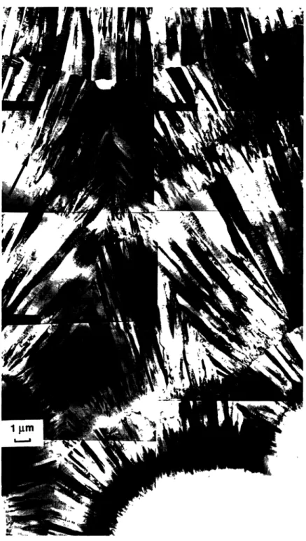
mode.Figure
2 shows such animage corresponding
to an arealocated near the fibres
constituting
thepreform
of thecomposite.
In this case, the fibres have theiraxes
parallel
to the incident beam andthey
have been eliminatedduring
the ionmilling operation.
Their transversal sections wereinitially
located where three circular holes are observed. Thecrystals
of theSiC(CVI)
matrix are columnar and growradially
from the surface of these fibreswith some
interruptions arising
from theprocessing.
Thus,
theSiC(CVI)
matrixappears
as anarrangement
of domains several micrometres across.They
are delineatedfirstly by
the boundaries betweencrystals
grown from different fibres andsecondly by
several zones concentric with the transversal section of the fibres and related to arupture
ofgrowth.
crys-Fig.
2. -Morphology
of theSiC(CVI)
matrix. The three holes of circularshape -
two at theright
bottom of theimage
and another one, but lessvisible,
at the left bottom - werepreviously occupied by
the transversal section of fibres. The three black arrows indicate the directionsof growth
of theSiC(CVI)
crystals
from the surface of the fibres.tals,
theboundary
zones and the areas where arupture
of growth
occurs. Thispaper
is concernedonly
withcrystals
that have been studied both from the chemical and structuralpoints
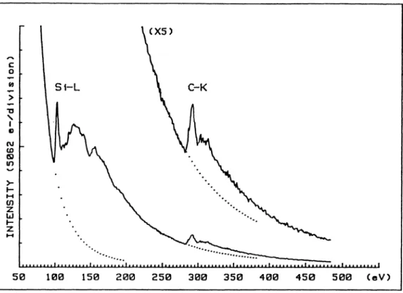
of view. 3.2 COMPOSITION. - The ratio of the number of silicon and carbon atoms(NSi/Nc)
in the columnarcrystals
has been checkedby
EELS. This ratio has been determinedby applying
aquan-titative treatment to the distributions
corresponding
to the Si-Ledge
to the C-Kedge
of theSiC(CVI) crystals
and of a 6Hsingle crystal,
withproper
thicknessconditions,
according
to thefollowing
relation[13]:
where
Ssi(a, ¡lE)
andSc( a, ¡lE)
are the areas under the Si-L and the C-K distributions above thebackground (Fig. 3)
and,
03C3Si(03B1, AE)
anduc( a, AE)
are thepartial
cross-sectionsintegrated
overthe collection
angle a
and the energy window AE. For thefollowing
experimental
conditions,
V =120 kV and a = 9.25
mrad,
the values of thepartial
cross-sections were: 0- si = 9.213 x10- 20
cm2
and uc = 6.157 x
10-21 cm2.
The value of the ratio obtained varies from 0.9 to 1.0 for thepolytypes
and isequal
to 0.9 for thesingle crystal. Taking
into account the 10% accuracyrecognized
for this kind of measurement, we can consider that thewell-developed
columnarcrystals
of the matrix arestoichiometric.
Fig.
3. - ElectronEnergy
Loss spectra of aSiC(CVI) crystal
(V
= 120kV,
a = 9.25mrad).
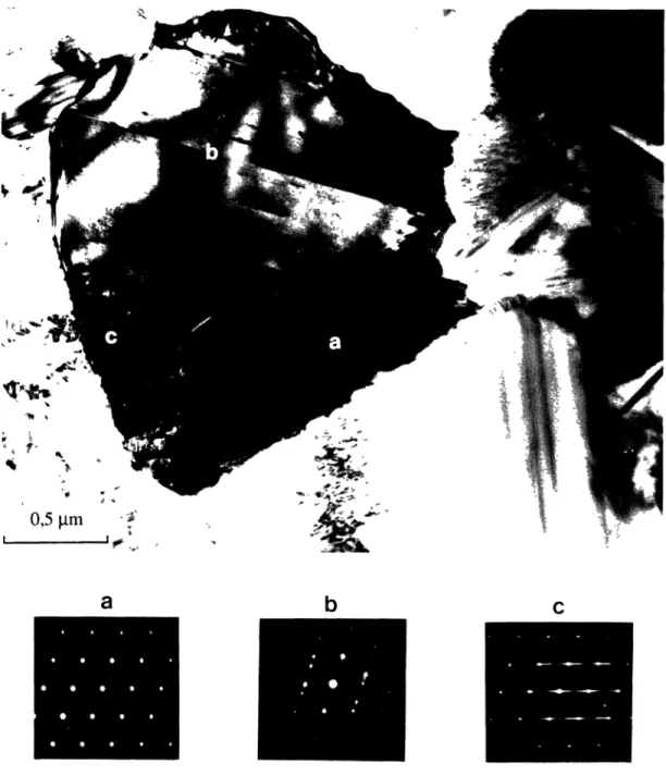
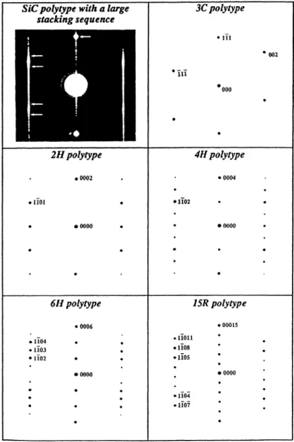
The dotted3.3 DIFFRACTION PATTERNS. - 1BB’0 kinds of diffraction
patterns
have been obtained. The firstcorresponds
to the cubicstructure,
which can beeasily
identified in this way. This structure maybe
perfect
3C structure(Fig. 4a),
twinned(Fig. 4b)
orheavily
faulted(Fig. 4c).
The second kind ofdiffraction
patterns
shows the same features as theheavily
faulted cubic one(Fig.
5)
but does notexhibit
strong
diffractionspots
at thepositions
wherethey
would beexpected
for the cubic struc-ture({111}, {002}).
Here,
thepositions
of theintensity
maxima could be attributed to those of both the cubic and thehexagonal
structures, as confirmedby
thecorresponding
simulated diffrac-tionpatterns.
From thesepatterns,
the nature of thepolytype
cannot bedirectly
identified,
but the continuousstreaking
of the reflexions associated with thestacking
direction indicates that thec
parameter
of thispolytype
is verylarge. Consequently,
twoassumptions
can beproposed:
either thestacking
is ordered and thepolytype
has a verylarge period
[14-16]
or there is noperiodicity
and the
polytype
is called"one-dimensionally-disordered"
[17-19].
3.4 HIGH RESOLUTION IMAGES. -
High
resolutionimages
aredependent
on numerousphysical
parameters,
such as themicroscope
characteristics(i.e. voltage, spherical
aberration and focusspread),
the conditions of observation(i.e.
defocus and beamdivergence),
and thesample
itself(i.e.
thickness andorientation). High
resolutionimage
interpretation
is notstraightforward.
The best way ofconfirming
theseinterpretations
is to relate theexperimental images
to simulated ones[7, 20-22].
This
procedure
was followed in the case of the structure shown infigure
6,
which has been extracted from anexperimental image.
This structure is observedalong
a1120 >
direction. It can be considered either as alarge period polytype
(N
=30)
with c = 7.5 nm or as apart
ofa
sequence
of a"one-dimensionally-disordered" polytype.
As shown infigure
6,
the simulated diffractionpattern
of this structure agreesperfectly
wit theexperimental
one shown infigure
5.The
images
of thispolytype
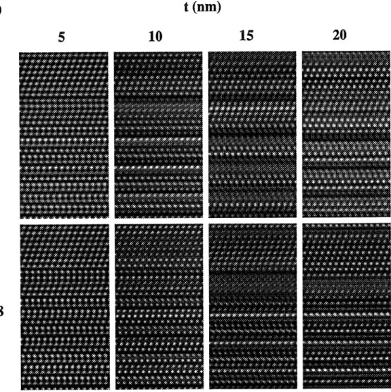
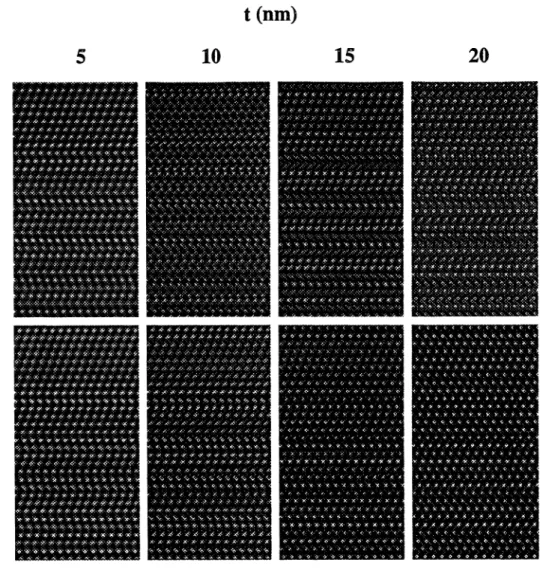
have been calculated for JEOL 200CX-S and PHILIPS CM30-STmicroscopes
with different thicknesses(5, 10, 15
and 20nm)
and defocus valuescorresponding
tothe two first
positive
andnegative passbands (Figs.
7 and 8respectively). They
may becompared
with theexperimental images
obtained with a JEOLmicroscope (Fig. 9)
and with a PHILIPSmicroscope (Fig. 10).
Figure
9 is characterizedby
bands
of different widthperpendicular
to thestacking
direction. Some of these contain whitedots,
wellseparated,
while othersappear
blurred. Such a feature is observed onnearly
all the simulationscorresponding
to the 200 kV situationexcept
for the 5 nmthickness
(Fig. 7).
It isnoteworthy
that these simulations were calculated for an axial illumination.The
possible
effect of aslight misalignment
of thespecimen [23]
isonly
toemphasize
such a feature as can be controledthrough
calculations. No conclusion can be deduced about the exact natureof the
polytype
from suchexperiments.
As shown
by
thesimulations,
theproblem
could be solved if the resolution were better. Thisis confirmed
by figure
10,
whichcorresponds
to anexperiment
on a CM30-STmicroscope.
From thecomparison
of simulations andfigure
10 theimage
is consistent with asample
thickness ofapproximately
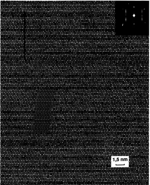
5 nm, with a defocus close to 78 nm.Figure
11,
which is anenlargement
offigure
10,
emphasizes
the excellentagreement
between theexperimental
and the calculatedimages.
Under theseconditions,
the white dots coincideexactly
with theprojected
SiC atomic columns(see
Fig. 1)
and the nature of thestacking along
the c direction can bedirectly
identified. In the case of thisSiC(CVI) crystal,
noperiodicity
has been observed in thestacking
over about a hundredFig.
4. -Bright
fieldimage
and electron diffractionpatterns
of SiC(CVI)
crystals
orientedalong
a 110 >direction. The
perfect (a),
twinned(b)
andheavily
faulted(c)
3C structures are observed.4. Conclusion and discussion.
Perfect,
twinned andheavily
faulted cubiccrystals
have beeneasily
identified in theSiC(CVI)
matrix ofSiC/SiC
composites through
their diffractionpatterns.
Fig.
5. - Simulated(3C,
2H, 4H,
6H and15R)
andexperimental
(SiC(CVI)
crystal)
diffractionpatterns
of SiC. Theintensity
maxima of theSiC(CVI)
(indicated by
arrows)
can be attributed to those of both the cubic and thehexagonal
forms of SiC(indexed
on thecorresponding
simulated diffractionpattern).
"One-dimensionally-disordered" polytypes
have also been identified in another area of thema-trix
by
HREMexperiments
and calculations. Suchpolytypes
werepreviously
observed in 1978by
Shinozaki et al. in chemical
vapour-deposited
silicon carbide[17-19].
Whenimaged
with about 1 nmresolution,
thesepolytypes
appear
as a distribution of lamellaeperpendicular
to thegrow-ing
direction.lbday,
theperformance
of modernhigh
resolution electronmicroscopes,
whose resolution is better than 0.2 nm, associated withimage
simulation,
render thestacking
sequence
of disorderedpolytypes directly interpretable.
Fig.
6. - Structure extracted from anexperimental image (Fig.
10 and11)
and thecorresponding
simulated diffraction pattern.This new situation encourages us to go further in the
understanding
of theapparent
irregularity
in thestacking
of thetetrahedral layers
of thesepolytypes.
Such anarrangement
appears
chaotic. Thepossibility
offollowing
directly
thestacking
order,
using high
resolutionimages,
is one wayFig.
7. - Simulatedimages
for the structure shown infigure
6 for the JEOL 200CX-Smicroscope
(voltage
V = 200kV;
spherical
aberrationCs
= 2 nm; beamdivergence (half-angle)
88 = 0.603mard;
focusspread
(rms)
bz = 7.1 nm;objective
aperture
cut-off at afrequency
u = 0.8Â-1).
Different thicknesses(t)
andFig.
8. - Simulatedimages
of the structure offigure
6 for the PHILIPS CM30-STmicroscope
(voltage
V = 300kV;
spherical
aberrationCs
= 0.9 nm; beamdivergence
(half-angle)
hO = 0.64mrad;
focusspread
(rms)
hz = 5.4 nm;objective
aperture u
= 0.8Â-1 ).
Same thicknesses(t)
as infigure
7. The values of the defocus(Az)
alsocorresponds
to the two firstpassbands.
Fig.
9. - JEOL 200CX-Shigh
resolutionimage
of aSiC(CVI)
crystal.
Blurred bandsprevent
the identifi-cation of thepolytype.
Fig.
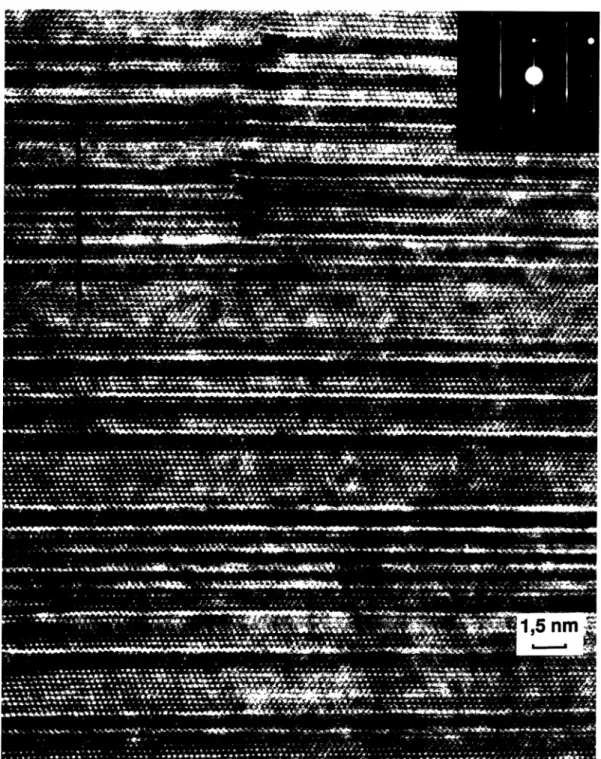
10. - PHILIPS CM30-SThigh
resolutionimage
of aSiC(CVI) crystal.
The white dots can bedirectly
correlated with the SiC atomic bicolumns(see Fig. 1).
Noperiodicity
is observed in thestacking
so that theFig.
11. -Enlargement
offigure
10 where thegood matching
between theexperimental
and the calculatedimages
of the structure offigure
6 isstriking.
References
![Fig. 1. - Structures of the cubic, 3C, and of one the hexagonal, 6H, forms of SiC respectively observed along the [110] and the [1120] direction](https://thumb-eu.123doks.com/thumbv2/123doknet/13708973.434256/4.723.133.560.103.649/fig-structures-cubic-hexagonal-forms-respectively-observed-direction.webp)
![[PDF] cours Diagrammes d'interaction UML | Cours informatique](data:image/gif;base64,R0lGODlhAQABAIAAAP///wAAACH5BAEAAAAALAAAAAABAAEAAAICRAEAOw==)