HAL Id: cea-01053384
https://hal-cea.archives-ouvertes.fr/cea-01053384
Submitted on 30 Jul 2014
HAL is a multi-disciplinary open access archive for the deposit and dissemination of sci-entific research documents, whether they are
pub-L’archive ouverte pluridisciplinaire HAL, est destinée au dépôt et à la diffusion de documents scientifiques de niveau recherche, publiés ou non,
Mixed metal dielectric gratings for pulse compression
Jerome Neauport, Gabriel Dupuy, N. Bonod, S. Hocquet, S. Palmier
To cite this version:
Jerome Neauport, Gabriel Dupuy, N. Bonod, S. Hocquet, S. Palmier. Mixed metal dielectric gratings for pulse compression. Optics Express, Optical Society of America - OSA Publishing, 2010, 18 (23), pp.23776-23783. �10.1364/OE.18.023776�. �cea-01053384�
Mixed metal dielectric gratings for pulse
compression
J. Neauport,1,* N. Bonod,2 S. Hocquet,1 S. Palmier,1 and G. Dupuy1 1Commissariat à l’énergie atomique, Centre d’études scientifiques et techniques d’Aquitaine,
BP 2, 33114 Le Barp, France
2Institut Fresnel, CNRS, Aix-MarseilleUniversité, Ecole Centrale Marseille, Domaine Universitaire de Saint Jérôme,
13013 Marseille, France
Abstract: We report on manufacturing and testing results of high efficiency
mixed metal dielectric gratings (MMLD) for high power pulse compression applications. The gratings with 1780 l/mm are etched in the top low index layer of a Au-(SiO2/HfO2)4-SiO2 mirror stack. Various grating profiles
manufactured in order to modify the near electric field distribution are damage tested on a facility operating at 1.053 µm, 500 fs pulse duration. We evidence that damage threshold is governed by the value of the maximum electric field intensity inside the grating pillar. Moreover thresholds close to 3 J/cm2 beam normal are obtained with this new MMLD grating being thus an interesting alternative to gold and pure dielectric gratings for pulse compression applications.
©2010 Optical Society of America
OCIS codes: (140.7090) Ultrafast lasers; (050.0050) Diffraction and gratings; (350.1820)
Damage; (350.2250) Femtosecond phenomena.
References and links
1. D. Strickland, and G. Mourou, “Compression of amplified chirped optical pulses,” Opt. Commun. 56(3), 219– 221 (1985).
2. N. Blanchot, and C. Rouyer, “Lasers femtosecondes de forte intensité et forte énergie,” in Lasers et technologies
femtosecondes, M. Sentis, O. Uteza, eds (Publications de l'Université de Saint Etienne, 2004), pp. 33–43.
3. B. C. Stuart, M. D. Feit, S. Herman, A. M. Rubenchik, B. W. Shore, and M. D. Perry, “Optical ablation by high power short-pulse lasers,” J. Opt. Soc. Am. B 13(2), 459–468 (1996).
4. M. D. Perry, R. D. Boyd, J. A. Britten, D. Decker, B. W. Shore, C. Shannon, and E. Shults, “High-efficiency multilayer dielectric diffraction gratings,” Opt. Lett. 20(8), 940–942 (1995).
5. B. C. Stuart, M. D. Feit, A. M. Rubenchik, B. W. Shore, and M. D. Perry, “Laser-induced damage in dielectrics with nanosecond to subpicosecond pulses,” Phys. Rev. Lett. 74(12), 2248–2251 (1995).
6. N. Bonod, and J. Neauport, “Optical performances and laser induced damage threshold improvement of diffraction gratings used as compressors in ultra high intensity lasers,” Opt. Commun. 260(2), 649–655 (2006). 7. S. Palmier, J. Neauport, N. Baclet, E. Lavastre, and G. Dupuy, “High reflection mirrors for pulse compression
gratings,” Opt. Express 17(22), 20430–20439 (2009).
8. N. Blanchot, E. Bar, G. Behar, C. Bellet, D. Bigourd, F. Boubault, C. Chappuis, H. Coïc, C. Damiens-Dupont, O. Flour, O. Hartmann, L. Hilsz, E. Hugonnot, E. Lavastre, J. Luce, E. Mazataud, J. Neauport, S. Noailles, B. Remy, F. Sautarel, M. Sautet, and C. Rouyer, “Experimental demonstration of a synthetic aperture compression scheme for multi-Petawatt high-energy lasers,” Opt. Express 18(10), 10088–10097 (2010).
9. N. Blanchot, G. Marre, J. Néauport, E. Sibé, C. Rouyer, S. Montant, A. Cotel, C. Le Blanc, and C. Sauteret, “Synthetic aperture compression scheme for a multipetawatt high-energy laser,” Appl. Opt. 45(23), 6013–6021 (2006).
10. J. Neauport, E. Lavastre, G. Razé, G. Dupuy, N. Bonod, M. Balas, G. de Villele, J. Flamand, S. Kaladgew, and F. Desserouer, “Effect of electric field on laser induced damage threshold of multilayer dielectric gratings,” Opt. Express 15(19), 12508–12522 (2007).
11. HORIBA Jobin Yvon SAS, 16–18 rue du Canal, 91165 Longjumeau cedex, France.
12. C. J. Stolz, J. R. Taylor, W. K. Eickelberg, and J. D. Lindh, “Effects of vacuum exposure on stress and spectral shift of high reflective coatings,” Appl. Opt. 32(28), 5666–5672 (1993).
13. R. Thielsch, A. Gatto, and N. Kaiser, “Mechanical stress and thermal-elastic properties of oxide coatings for use in the deep-ultraviolet spectral region,” Appl. Opt. 41(16), 3211–3217 (2002).
14. T. Z. Kosc, A. A. Kozlov, and A. W. Schmid, “Formation of periodic microstructures on multilayer dielectric gratings prior to total ablation,” Opt. Express 14(22), 10921–10929 (2006).
1. Introduction
The Chirped Pulse Amplification (CPA) technique proposed in 1985 by Stickland and Mourou [1] strongly impacted the laser community and permitted to highly enhance the fluence of femtosecond pulse [2]. Diffraction gratings are good candidates for stretching and compressing laser pulses; and the development of Ultra High Intensity (UHI) laser systems of increasing performances all around the world is currently pushing grating performances to new extent. The half meter to meter scale pulse compression gratings used in vacuum compressors of such CPA laser systems must comply with many different constraints. First, they must exhibit high and uniform diffraction efficiencies in the 1st reflected order; e.g. mean efficiencies of more than 95% can be obtained with multilayer dielectric gratings. Secondly, they must present low aberrations in this reflected order; e.g. a few hundred of nanometers can be obtained on half meter scale parts. Thirdly, they shall keep their integrity during air/vacuum cycles. This specific constrain is of peculiar importance for multilayer dielectric gratings. Finally, they shall sustain high fluence in short pulse regime. Values of 1 J/cm2 to some J/cm2 at wavelengths of 800nm or 1053nm for picoseconds or down to a few tenths of femtoseconds are requested depending on the laser facility.
The first CPA laser systems used gold gratings. But the rather low diffraction efficiency and limited damage threshold [3] of such gratings limit the performances of these facilities. Multilayer dielectric gratings (MLD) were proposed and developed at Lawrence Livermore National Laboratory by Perry et al. in 1995 [4]. A MLD grating consists in a mirror stack made of alternative low and high refractive index dielectric materials with a grating engraved in its top layer. This type of grating offers the benefit of having up-rated diffraction efficiency and high damage threshold around the wavelength of 1µm thanks to the use of dielectric material instead of metal [5]. As it is the case with dielectric mirrors, multiple layers of dielectrics used in the MLD grating are prone to crazing when exposed to vacuum. Usually, this problem is solved by optimizing the deposition process. Since crazing is due to stress in the dielectric stack and that stress is proportional to the whole stack thickness, we have proposed in a previous work to limit this quantity [6]. This Mixed Metal Dielectric grating (MMLD) is obtained by adding a gold reflective layer below a very limited number of pairs of low and high refractive index dielectric layers. The grating is engraved in an additional SiO2
top layer. We evidenced that this technique permits to reduce the number of pairs down to 3 together with preserving the gold surface from a high electric field intensity. The strong reduction of the electric field intensity through the reduced mirror stack permits to achieve high reflected efficiencies higher than 96%. The electric field enhancement in the top engraved layer was reduced by increasing the groove width (i.e. by reducing the pillar width) [6]. More recently we made an experimental measurement of the laser induced damage threshold of the mirror stacks used in both MLD and MMLD gratings. We demonstrated that both mirrors exhibit similar performances [7] evidencing that the additional gold layer of the MMLD design does not lower damage performances.
Hereafter, we present results on full MMLD gratings. MMLD gratings were manufactured to comply with the specification of the PETAL facility [8]. Let us remind that this facility uses a synthetic aperture compression scheme [9] with 1780 l/mm gratings illuminated at an incidence of 77.2° at the wavelength of 1.053 µm in TE polarization. Pulse duration on the last grating of the compressor is 500 fs. Grating design, manufacturing and characterization are detailed in Section 2. We then discuss the results in Section 3 and finally offer our conclusions.
2. Numerical simulations
Our first aim was to optimize MMLD gratings to fulfil PETAL compressor requirements (1780 l/mm, 77.2° incidence, TE polarization). This optimization was done using numerical simulations that have been presented in [6]. The numerical treatment is made with the use of the differential method which resolves Maxwell equations in periodic media. It allows the
calculation of the diffraction efficiencies in the various orders of the grating as well as the accurate calculation of the near electric field intensity in the periodic structure.
We evidenced previously that only 3 to 4 pairs of low index and high index dielectrics were sufficient to reduce the amount of energy impinging the gold layer of the MMLD grating [6]. In the present work, we selected a Au-(LH)4L design where high and low index materials are chosen to be HfO2 and SiO2 respectively. Such a design is a good trade-off to achieve a
reflectivity higher than 99% at 1053nm under vacuum for an incidence of 70.6° (average angle between the (0)th and the 1st order of the final 1780 l/mm grating). The retained design of the mirror is the following: 20nm Cr 150nm Au (232nm SiO2 157nm HfO2)4 574nm SiO2
and the grating is then to be engraved in the 574 nm silica top layer. The grating profile is characterized by the duty cycle DC = 1 - c1/2/d, the groove height h, the residual thickness of
the silica layer e, and the angle of pillars slope α considering assuming a trapezoidal geometry as depicted on Fig. 1.
h
e
c1/2
Mixed metal dielectric stack H
d
Fig. 1. A silica layer of thickness H is coated on a MMLD mirror reflecting more than 99% of the incident light ( = 1053 nm and θ = 70.6°). A grating is ion etched in the silica layer with a period d, a groove height h, and a groove width at the half depth c1/2. The residual thickness of
the silica layer is denoted e. Pillars present a trapezoidal geometry with angle of slope α taken equal to 83° in the whole manuscript.
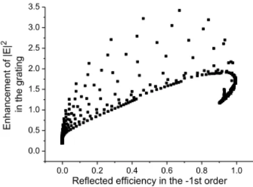
We can then calculate both 1st reflected order diffraction efficiency and maximal value of the electric field enhancement in the solid material for the all possible {h, DC} couples. Such a diagram is presented on Fig. 2 where each dot on the plot represent an {h, DC} couple when h varies from 0 to 574 nm, DC varies from 0.2 to 0.6. It can be seen that with such a design, low electric field enhancements around 1.25 can be obtained together with high diffraction efficiencies close to 94%.
0.0 0.2 0.4 0.6 0.8 1.0 0.0 0.5 1.0 1.5 2.0 2.5 3.0 3.5 E nhance m ent of |E | 2 in t he grat ing
Reflected efficiency in the -1st order
Fig. 2. Maximum value of the enhancement of the electric field |E|2 in the solid material
normalized by the incident field |E0|2 as a function of the reflected efficiency. An enhancement
of about 1.25 can be obtained for efficiencies close to 94%.
From these results, the best grating design can be selected to get a high diffraction efficiency and a high laser damage threshold. The grating profile is optimized in order to maximize the reflection efficiency and to minimize the electric field enhancement [10].
3. Experimentals and discussions
3.1. Sample manufacturing and characterization
On the basis of the numerical optimization performed at the Fresnel Institute, the samples were manufactured on 120 × 140 × 15 Pyrex substrates. Coating was done by CEA LITEN using an Electron Beam Physical Vapor Deposition (EBPVD) process. A full description of deposition conditions is available in [7]. The reflectivity of each manufactured sample was then measured and the physical thicknesses of the various layers were then numerically fitted from the measured curves. Uncertainty on the obtained thicknesses is estimated to less than 1%. The resulting final stacks are presented in Table 1.
Table 1. Fitted design for each sample. Quantities in nanometres are physical thicknesses of each layer
Serial number Fitted design
06-0675 20nm Cr 150nm Au (225nm SiO2 157nm HfO2)4 558nm SiO2 06-0676 20nm Cr 150nm Au (235nm SiO2 155nm HfO2)4 580nm SiO2
06-0679 20nm Cr 150nm Au (235nm SiO2 155nm HfO2)4 580nm SiO2
Gratings were finally etched in the silica top layer of the deposited mirrors by Horiba Jobin Yvon [11]. Three samples were manufactured using various grating profiles. The groove profiles were then controlled by atomic force microscopy (AFM) at the position where the damage testing shall be conducted. Measurements on calibrated references have shown that uncertainty on h is +/3% and +/0.03 on c1/2/d ratios. Diffraction efficiencies were also controlled at the same location at an incidence of 77.2° and wavelength of 1053nm in TE polarization on a dedicated scanning photometer on the whole clear aperture of the part with a 2mm × 4mm sampling step. Taking into account the real grooves profiles measured by AFM, calculations were performed to get the normalized electric field intensity |E/E0|2 in the top
modulated area. These measurements are summarized in Table 2.
Table 2. MMLD grating manufactured. (1) diffraction efficiency measurements are in good agreement with simulations. Diffraction efficiency and grating profile are given at
the position of the future damage test
Serial
number α e (nm) h (nm) DC
(1) reflected order diffraction efficiency, measured / calculated |E/E0|2 maximum calculated in the MMLD, TE, 77.2° 06-0675 80° 164 394 0.346 96.7% / 99.2% 1.71 06-0676 81° 180 400 0.365 96.3% / 95.5% 1.97 06-0679 78° 124 456 0.357 96.9% / 97.2% 1.59
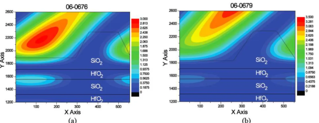
The electric field intensity distribution in the top area of the grating is displayed in Fig. 3 for two manufactured gratings which present pronounced difference between of |E/E0|2
maximum values. One can see that for both gratings, the maximum intensity occurs in the grating pillar. Same results have already been observed with MLD gratings designs [10].
Fig. 3. Reconstitution of |E/E0|2 in the top area of gratings 06-0676 (a), and 06-0679 (b)
respectively.
3.2. Stress management of MMLD coatings
Gratings used for Petal pulse compression operate under high-vacuum environment (3.2 × 10⁶ mBar). A vacuum exposure modifies the stress on coatings which can cause crazings in some catastrophic cases [12]. A reduction of the coating thickness is attended to reduce the stress impact on gratings [10] and we have compared MLD and MMLD structures on crazing phenomena. Two samples of MLD and MMLD stacks have been exposed to a few air/vacuum cycles to test there sensitivity to crazing (1 Atm, ambient temperature, 5.106mBar). Both stacks use the same EBPVD process (LITEN coatings) and the only difference is the number of SiO2/HfO2 layers. After a few cycles, samples are observed using an intense fiber lamp. We
observe that the MLD stack is very sensitive to crazing and that a few fractures appeared after the first air/vacuum cycles while the MMLD stack keeps its surface integrity. Even though MLD alternative deposit methods may solve some crazing issues [13], the thickness reduction offered by the MMLD technique can be an alternative option for stress considerations for a given deposit method. Moreover, both approach could also be combined.
3.3. Laser induced damage measurements
The laser damage resistance study was experimentally made with the so-called DERIC set-up developed at the CEA/CESTA. This facility has already been presented in detailed in [10] and we briefly remind in this manuscript the main parameters. DERIC is characterized by a Gaussian laser beam with wavelength of 1057 nm, pulse duration of 500 fs, a diameter of 200
m at 1/e2
on the sample. The repetition rate is 10 Hz. Fluences are always given in beam normal with a precision of ± 9%. The operator detects the damages thanks to a long working
distance microscope equipped with CCD camera (resolution of about 10 m). Tests are
performed at a temperature of 20°C under dry air (RH<10%).
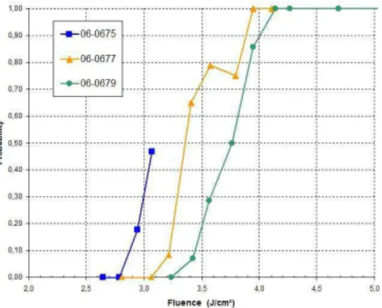
Before testing, samples were cleaned by a drag wipe method with ethanol. The test mode is S on 1. Depending on the sample behaviour during the damage test, from 10 to 40 sites are exposed to a burst of 100 laser pulses at a specified fluence. Then each damage site is counted in order to get a damage probability. This operation is repeated for different fluences; at the end, about 200 sites are tested to get the whole damage probability curve. From theses results, the laser induced damage threshold, i.e. the highest fluence value for which no damage is detected, is determined. The three grating samples were tested on the DERIC set-up at the incidence angle of 77.2° in TE-polarization.
Fig. 4. Damage probability of MMLD gratings. 1057nm, 500fs, TE polarization, at the incidence of 77,2°. Fluences are given in beam normal.
Figure 4 shows that damage threshold measured for each sample is about 3 J/cm2. This value can be compared with threshold measurements performed on similar 1780 l/mm MLD gratings which exhibited damage threshold about 4.5 J/cm2 [10]. Our previous work was focused on the comparison between MMLD and MLD mirror stack and we evidenced that their damage performances were similar as long as the electric field distribution was taken into account to correct the data [7]. And it is still questionable if this assertion shall apply in the case of gratings.
Figure 5 gives the dependence of the damage threshold with the electric field enhancement for the MMLD grating herein studied. Thresholds are obtained from Fig. 4 while the electric field enhancement is obtained from Tab. 1. Let us emphasize that both damage measurements and grating profile AFM measurements that lead to the calculations of light intensity are made on the same area. Those results can be compared with results obtained on MLD gratings [10]. We have already shown that the value of electric field enhancement is correlated to the damage threshold for MLD gratings [10]. It is still the case for MMLD gratings but a clear shift between the MLD and MMLD grating curves is observed. We believe that this shift is induced by the difference of coating manufacturers and then EBPVD process parameters since MLD gratings from [10] were made on SAGEM coatings while MMLD gratings were made on LITEN coatings.
Fig. 5. Damage performance at 1.053 m, TE polarization, 500 fs versus 1/|E/E0|2 in the solid
material on three different MMLD samples tested at 77.2°. Damage threshold is proportional to the inverse of the electric field enhancement. Comparison with MLD grating [10] is also
One can notice that the field enhancement in the MMLD samples is still rather high (1.57 for 06-0679) while compared to previous MLD gratings (1.4 for PW08 sample [10]). Figure 1 shows that, with the retained MMD design, the field enhancement could be reduced down to 1.25 with lower DC. Since the damage threshold appears to be related to the electric field enhancement, further improvements should be gained by optimizing the grating profile and reducing the pillar width. We should then expect similar MMLD and MLD grating damage behaviour.
We also have studied the damage morphology on MMLD gratings. Damages were observed on a ZEISS Axio Imager A2m microscope equipped with x20, x50 and x100 objectives in circular difference interference contrast mode. Since a S on 1 testing mode with 100 shots per site is used, damage created exhibit both initiation and some growth depending on when damage initiate during the 100 shots sequence. Results are presented in Fig. 6. Damage growth is similar to the one observed on MLD gratings [10]. Damages initiate on the SiO2 groove layer, as it can be seen in Fig. 6(a) showing a typical damage initiation with some
rather limited growth. They evolve in width and depth [the HfO2 layer is damaged in
Fig. 6(b)] and then reach the gold substrate [Fig. 6(c)]. Specifically, ripple structures perpendicular to the grating lines [see Fig. 6(d)] are easily observed on every damage periphery. The period of the ripples is approximately 2.5µm. This phenomenon has often been observed on MLD gratings [10,14].
Fig. 6. Damage morphology on MMLD grating sample 06-0676 at different stages of the damage: the initiation with some limited growth [Fig. 6(a)], subsequent growth [Fig. 6(b)], the damage for the highest fluence tested [Fig. 6(c)]. Figure 6(d) is a zoom of the damage from Fig. 6(c) made with the x100 microscope objective.
4. Conclusion
It has been evidenced that a judicious combination of metal and dielectric materials provides highly efficient gratings. Efficiencies as high as 96% have been recorded on 1780 l/mm MMLD gratings illuminated at incidence of 77.2° in TE polarization with 500 fs pulse duration. Furthermore, these gratings samples were damage in operating conditions and they
exhibited damage threshold close to 3 J/cm2. The threshold is seen to be governed by the maximum value of the electric field enhancement in the solid material. The damage initiates on the top silica layer were this enhancement is maximal. Hence, modifying grating structure should improve performances to threshold similar to MLD grating.
Acknowledgments
This work is supported by the Conseil Régional d’Aquitaine, the French Ministry of Research and the European Union, and is performed under the auspices of the “Institut Lasers et Plasmas” (ILP). DERIC damage testing facility development was performed under the auspices of Laserlab-Europe program. We thank the ALISÉ team for access to and modular capabilities of ALISÉ facility. We also would like to warmly thank people from HORIBA Jobin Yvon for grating manufacturing, N. Baclet from CEA Liten for mixed mirror manufacturing, and J Kolopp for air/vacuum cycles on samples.