HAL Id: hal-00257982
https://hal.archives-ouvertes.fr/hal-00257982
Submitted on 20 Feb 2008
HAL is a multi-disciplinary open access
archive for the deposit and dissemination of
sci-entific research documents, whether they are
pub-lished or not. The documents may come from
teaching and research institutions in France or
abroad, or from public or private research centers.
L’archive ouverte pluridisciplinaire HAL, est
destinée au dépôt et à la diffusion de documents
scientifiques de niveau recherche, publiés ou non,
émanant des établissements d’enseignement et de
recherche français ou étrangers, des laboratoires
publics ou privés.
A 6-GHz Low-Power BiCMOS SiGe:C 0.25 µm Direct
Digital Synthesizer
Stéphane Thuries, Éric Tournier, Andreia Cathelin, Sylvain Godet, Jacques
Graffeuil
To cite this version:
Stéphane Thuries, Éric Tournier, Andreia Cathelin, Sylvain Godet, Jacques Graffeuil. A 6-GHz
Low-Power BiCMOS SiGe:C 0.25 µm Direct Digital Synthesizer. IEEE Microwave and Wireless
Components Letters, Institute of Electrical and Electronics Engineers, 2008, 18 (1), pp.46 - 48.
�10.1109/LMWC.2007.911994�. �hal-00257982�
1
A 6-GHz Low-Power BiCMOS SiGe:C 0.25 µm
Direct Digital Synthesizer
St´ephane Thuries, ´
Eric Tournier, Andreia Cathelin, Sylvain Godet and Jacques Graffeuil Member, IEEE
Abstract— A 6-GHz low power SiGe direct digital synthesizer
(DDS) is reported. This paper discusses the BiCMOS design improvements used for the phase accumulator and the phase-to-amplitude conversion in order to achieve higher speed operation and lower power consumption compared to existing DDS. The phase accumulator is based on a three-level BiCMOS logic, and the phase-to-amplitude conversion is completed through a bipolar differential pair. The circuit has been processed in a BiCMOS SiGe:C 0.25 µm technology. The power consumption is 308 mW and it operates from a 2.8 V supply. The chip core area is 1 mm2.
I. INTRODUCTION
A Direct Digital Synthesizer (DDS) [1] is a very versa-tile signal generation block, known to have many attractive characteristics among which are fast settling time, possible high frequency resolution, phase and frequency modulation capabilities and large bandwidth. All these features make DDS very attractive for modern microwave telecommunication systems. Although the principle of DDS has been known for many years, it did not get a dominant role in microwave communication systems due to its frequency limitation and/or high power consumption.
The block diagram of the traditional DDS architecture is shown in Fig. 1. It consists of a phase accumulator, a phase-to-amplitude converter (ROM) and a digital-to-analog (D/A) converter. In this paper, we present a fully integrated 6-GHz DDS. This DDS does not only operate at the highest clock frequency on a silicon technology that has been reported to our knowledge, but also demonstrates a considerably reduced power consumption. Two techniques are used in order to achieve theses goals :
• the phase-to-amplitude conversion is performed from an analog triangle-to-sine conversion based on the non-linear transfer function of a bipolar differential pair.
• the digital blocks and particularly the phase accumulator are implemented in a 3-levels merged CMOS/bipolar-ECL logic.
II. DDS ARCHITECTURE
A. Bipolar Differential Pair Phase-to-Amplitude Converter
The proposed DDS 9-bits architecture is based on the idea that the non-linear transfer function of a bipolar differential
Manuscript received september, 2006; revised august, 2007. This work was supported by ST Microelectronics.
St´ephane Thuries, ´Eric Tournier, Sylvain Godet and Jacques Graffeuil are with the LAAS/CNRS research laboratory and with the Paul Sabatier university, Toulouse, 31077, France (email: sthuries@laas.fr; tournier@laas.fr; graffeui@laas.fr). Andreia Cathelin is with ST Microelectronics, Crolles, 38926, France (email: Andreia.Cathelin@st.com)
FCW R eg is te r I I I I I R O M D A C L P F Phase accumulator A d d er
Fig. 1. Traditional DDS architecture
FCW R eg is te r 9 9 9 9 9 D iff er en tia l L in ea r D A C L P F Phase accumulator C o m p le m en te r MSB 8 8 Bip o la r D iff er en tia l P ai r A d d er A B
Fig. 2. DDS architecture of the proposed phase to amplitude converter
pair can be pertinently used in order to convert a triangle wave into a sine wave [2], [3]. The DDS resultant architecture is shown in Fig. 2. It consists of a phase accumulator, a complementer, a D/A converter and a bipolar differential pair. The frequency control word (FCW) is repeatedly added to the accumulator contents, generating a digital ramp which represents the instantaneous phase of the output signal. The most significant bit (MSB) is used to decode the half wave symmetry property of the sine wave: the MSB controls a
n − 1 bits complementer which transforms the phase ramp
into a digital triangle. The D/A converter translates this digital triangle into two differential analog ones. Finally, the bipolar differential pair transforms the differential analog triangle into an analog sine wave as shown in Fig. 3. The resistor between the two transistor emitters used in [2] has been safely removed because we use here one collector as a single output.
Gnd i Analog triangle from DAC Output signal Transfer function Vdd Vin(V) Vin Vout(V) Vout
2 (a) (b) Ai Ai Bi Bi Bi Bi Ci Ci Rsum Rsum Ai Ai Bi Bi Ci Ci Ci Ci Rsum Rsum Level 1 Level 2 Level 3 Ibias Q1 M1 Q2 M2
Fig. 4. Bipolar half adder (a) and merged bipolar/NMOS half adder (b)
B. BiCMOS Phase Accumulator
Typically the conventional phase accumulator designs that provide the highest speed capability are based on ECL adder [4], [5]. These designs are not suitable for wireless telecommunications systems due to their high power consump-tion and the use of high cost technologies. SiGe BiCMOS technologies are now considered as mid-cost while they pro-vide both high-speed Heterojuntion Bipolar Transistors (HBT) and CMOS transistors. Merged CMOS/Bipolar current switch logic (MCSL) has been suggested [6] in order to reduce the adder power consumption. The 3-levels series BiCMOS phase accumulator proposed in this paper consists of a nine-bits ripple adder followed by a 9-nine-bits register. In a phase accumulator (Fig. 2) the adder inputs are not used identically: one (A) is used to control the phase increment and the other (B) is connected to the register output. The A input is constant most of the time as long as the output frequency is kept fixed. Then, in order to reduce the supply voltage and the power consumption, the lower level switches (Q1,Q2) and
the current source (Ibias) from the bipolar adder (Fig. 4 (a))
have been merged into two NMOS (M1,M2) controlled current
sources (Fig. 4 (b)). These sources are complementary driven according to the adder input. The power consumption for this 3-level, BiNMOS (Bipolar + NMOS) adder versus three-levels bipolar ECL is about 30% less because the Vdsvoltage needed
for the NMOS current source is very low compared to the voltage needed by the bipolar level (Vcemin= 0.8 V ) and the
current source. This modification does not affect the maximum operating frequency, nor the rejection of supply and process variations. The adder speed is limited by the carry propagation time, so by the level 3 bipolar transistor characteristics.
III. MEASUREMENTS ANDRESULTS
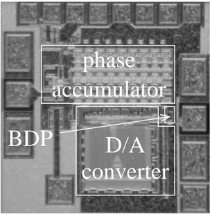
The proposed 9-bits DDS with an on chip 8-bits current steering D/A converter has been implemented in ST Micro-electronics 0.25 µm BiCMOS SiGe:C process that provide HBT with a Ft about 70 GHz. The die microphotograph is
shown in Fig. 5. The chip size is 1 × 1 mm2 with an active circuit size of 600 × 700 µm2. It consumes 308 mW and operates from a 2.8 V supply. The DDS chip operates up to a 6 GHz clock frequency and has been probing on wafer. Shown
accumulator
phase
BDP
converter
D/A
Fig. 5. Microphotograph of the DDS (BDP: Bipolar Differential Pair)
0.075 0.100 0.050 0.025 0 −0.025 −0.100 −0.050 −0.075 −0.125 0 20 40 60 80 100 120 140 160 180 Time (ns) O u tp u t (V )
Fig. 6. DDS output for FClk= 6 GHz and Fout= 11.71 MHz (FCW=1)
in Fig. 6 is the measured output waveforms at 11.71 MHz
corresponding to a frequency clock of 6 GHz with a FCW of 1. Fig. 7 shows the corresponding measured spectrum. The spurious free dynamic range (SFDR) versus FCW for three clock frequency is shown Fig. 8. At clock frequencies of 1 and 3 GHz, the SFDR is better than 31 dBc, and at a clock frequency of 6 GHz, the SFDR is better than 25 dBc for half of the FCW values. The Fig. 9 shows the harmonics level at the bipolar differential pair output versus the input triangle amplitude. This triangle-to-sine conversion provides a good harmonic rejection : −48 dBc, −74 dBc, −60 dBc and −43 dBc for the first, the second, the third and the fourth harmonics respectively.
IV. SUMMARY
In order to push the DDS beyond its traditional limits regarding the maximum operating frequency and power con-sumption, we have revisited the design of two of its main blocks. Firstly we have substituted an analog differential pair to any ROM-RAM or digital computation block used to convert the phase into amplitude. This drastically saves chip area and power consumption. Moreover, the maximum oper-ating frequency is now only limited by the phase-accumulator
3
TABLE I
COMPARISON OFDIFFERENTDDS ICS
Chip Process Clk frequency Accumulator Power Core area
(MHz) size (bits) (mW) (mm2) (MHz / mW)
Xuefeng [7] 0.35 µm CMOS 2000 8 820 3.99 2.43
Saul [8] 1 µm Bipolar Si 2500 31 5000 20 0.5
Dai [9] 0.35 µm BiCMOS SiGe 5000 8 2000 2 2.5
Guitierrez [10] Bipolar InP 9200 8 15000 40 0.613
Turner [11] Bipolar InP 13000 8 5420 3.92 2.39
This work 0.25 µm BiCMOS SiGe 6000 9 308 1 19.48
−20 −30 −40 −50 −60 −70 −80 −90 −100 10 20 30 40 50 60 70 Frequency (MHz) M ag n it u d e (d B m )
Fig. 7. DDS output spectrum for FClk= 6 GHz and Fout=11.71 MHz
(FCW=1) 15 20 25 30 35 40 45 0 50 100 150 200 250
Frequency control word [0:255]
S F D R (d B c) FClk= 1 GHz FClk= 3 GHz FClk= 6 GHz
Fig. 8. SFDR versus FCW for FClk= 1, 3 and 6 GHz
−10 −20 −30 −40 −50 −60 −70 −80 0.06 0.08 0.10 0.12 0.14 0.16 0.18 0.20 Triangle amplitude (V) H ar m o n ic s m ag n it u d e (d B c) First Second Third Fourth
Fig. 9. Output harmonics magnitude versus triangle amplitude applied to the differential pair
speed. Secondly, the traditional four-levels phase accumulators switches and bipolar current sources have been successfully merged into two NMOS current sources: this provides a 3-levels design featuring a 30% additional power consumption reduction. The proposed 9-bits DDS has been processed using a 0.25 µm SiGe:C BiCMOS technology and is fully functional
with a 308 mW power consumption. To our knowledge this is the first on-silicon DDS supporting a 6 GHz clock frequency. Further improvements should be done on the SFDR which remains a bit high at the full speed.
ACKNOWLEDGMENT
The authors would like to thank ST Microelectronics for providing the technology.
REFERENCES
[1] J. Tierney, C. Rader, and B. Gold, “A digital frequency synthesizer,” Audio and Electroacoustics, IEEE Transactions on, vol. 19, no. 1, pp. 48–57, 1971.
[2] R. Meyer, W. Sansen, and S. Peeters, “The differential pair as a triangle-sine wave converter,” Solid-State Circuits, IEEE Journal of, vol. 11, no. 3, pp. 418–420, 1976.
[3] S. Thuries and E. Tournier, “A DDS-oriented phase-to-amplitude con-verter using a SiGe:C bipolar transistors differential pair,” in Radio-Frequency Integration Technology: Integrated Circuits for Wideband Communication and Wireless Sensor Networks, 2005. Proceedings. 2005 IEEE International Workshop on, 2005, pp. 211–214.
[4] T. Mathew, S. Jaganathan, D. Scott, S. Krishnan, Y. Wei, M. Urteaga, M. Rodwell, and S. Long, “2-bit adder: carry and sum logic circuits at 19 GHz clock frequency in InAlAs/InGaAs HBT technology,” Electronics Letters, vol. 37, no. 19, pp. 1156–1157, 2001.
[5] S. Turner, J. Elder, R.B., D. Jansen, and D. Kotecki, “4-bit adder-accumulator at 41-GHz clock frequency in InP DHBT technology,” Microwave and Wireless Components Letters, IEEE, vol. 15, no. 3, pp. 144–146, 2005.
[6] W. Heimsch, B. Hoffmann, R. Krebs, E. Mullner, B. Pfaffel, and K. Ziemann, “Merged CMOS/bipolar current switch logic (MCSL),” Solid-State Circuits, IEEE Journal of, vol. 24, no. 5, pp. 1307–1311, 1989.
[7] X. Yu, F. Dai, Y. Shi, and R. Zhu, “2 GHz 8-bit CMOS ROM-less direct digital frequency synthesizer,” in Circuits and Systems, 2005. ISCAS 2005. IEEE International Symposium on, 2005, pp. 4397–4400 Vol. 5. [8] P. Saul and D. Taylor, “A high-speed direct frequency synthesizer,”
Solid-State Circuits, IEEE Journal of, vol. 25, no. 1, pp. 215–219, 1990. [9] F. Dai, L. Chimakurthy, D. Yang, J. Huang, and R. Jaeger, “A low power
5 GHz direct digital synthesizer designed in SiGe technology,” in Silicon Monolithic Integrated Circuits in RF Systems, 2004. Digest of Papers. 2004 Topical Meeting on, 2004, pp. 21–24.
[10] A. Gutierrez-Aitken, J. Matsui, E. Kaneshiro, B. Oyama, D. Sawdai, A. Oki, and D. Streit, “Ultrahigh-speed direct digital synthesizer using InP DHBT technology,” Solid-State Circuits, IEEE Journal of, vol. 37, no. 9, pp. 1115–1119, 2002.
[11] S. Turner and D. Kotecki, “Direct digital synthesizer with ROM-less architecture at 13-GHz clock frequency in InP DHBT technology,” Microwave and Wireless Components Letters, IEEE, vol. 16, no. 5, pp. 296–298, 2006.