HAL Id: hal-02958187
https://hal.archives-ouvertes.fr/hal-02958187
Submitted on 5 Oct 2020
HAL is a multi-disciplinary open access
archive for the deposit and dissemination of sci-entific research documents, whether they are pub-lished or not. The documents may come from teaching and research institutions in France or abroad, or from public or private research centers.
L’archive ouverte pluridisciplinaire HAL, est destinée au dépôt et à la diffusion de documents scientifiques de niveau recherche, publiés ou non, émanant des établissements d’enseignement et de recherche français ou étrangers, des laboratoires publics ou privés.
Distributed under a Creative Commons Attribution - NonCommercial| 4.0 International License
Waveguides
Marc Margalef-Rovira, J. Lugo-Alvarez, A. Bautista, L. Vincent, S. Lepilliet,
Abdelhalim Saadi, Florence Podevin, Manuel J. Barragan, Emmanuel
Pistono, Sylvain Bourdel, et al.
To cite this version:
Marc Margalef-Rovira, J. Lugo-Alvarez, A. Bautista, L. Vincent, S. Lepilliet, et al.. Design of mm-Wave Slow-wave Coupled Coplanar mm-Waveguides. IEEE Transactions on Microwave Theory and Tech-niques, Institute of Electrical and Electronics Engineers, 2020, �10.1109/TMTT.2020.3015974�. �hal-02958187�
Abstract— This paper focuses on the design of
high-performance Coupled Slow-wave CoPlanar Waveguide (CS-CPW) in CMOS technologies for the mm-wave frequency bands. First, the theory as well as the electrical model of the CS-CPW are presented. Next, the analytical approach for the calculation of the model parameters is discussed. Then, by using the developed model, two millimeter-wave backward directional 3-dB couplers are designed in a Bipolar Complementary-Metal-Oxide-Semiconductor (BiCMOS) 55-nm technology for 120 and 185-GHz operation, respectively. Simulation and experimental results demonstrate that the use of the CS-CPW concept leads to state-of-the-art performance, with a good agreement between the analytical model, electromagnetic simulations and measurement results.
Index Terms—CMOS/BiCMOS technology, coupling coefficient, directional couplers, slow-wave concept
I. INTRODUCTION
Nowadays, the need of high data-rates in a wide variety of applications such as novel communication standards, high-resolution radars, imaging systems for medicine and security, etc. pushes the electronic industry to the mm-wave frequency bands. In that context, the recent advances in CMOS and BiCMOS technologies have made them viable alternatives to GaAs or InP technologies. Current nanometric CMOS and BiCMOS transistors feature a fmax – ft higher than 300 GHz [1], but at a lower fabrication cost than their GaAs or InP counterparts. However, while active circuits offer a high performance in these technologies, the development of state-of-the-art passive circuits remains a challenging task. Beyond about 50 GHz, lumped circuits, such as baluns, couplers, power dividers, etc, based on capacitances, inductances and transformers, suffer from increased design complexity due to M. Margalef-Rovira and M. J. Barragan are with TIMA, CNRS, Grenoble INP, Université Grenoble Alpes, 38000 Grenoble, France (e-mail: [email protected]; [email protected]).
J. Lugo-Alvarez is with CEA, LETI, Univ. Grenoble Alpes, 38000 Grenoble France (e-mail: [email protected]).
A. Bautista is with Advanced Silicon, Lausanne, Switzerland (e-mail: [email protected]).
L. Vincent is with Grenoble INP, 38000 Grenoble, France (e-mail: [email protected])
M. Margalef-Rovira, A.A. Saadi, F. Podevin, E. Pistono, S. Bourdel, and P. Ferrari are with the RFIC-Lab, Grenoble INP, Université Grenoble Alpes,
parasitic effects that can no longer be neglected, but which are complex to model. Moreover, the quality factor of lumped components decreases with frequency, especially for Metal-Insulator-Metal (MIM) and Metal-Oxide-Metal (MOM) capacitors.
In this scenario, distributed circuits become a better option than the traditional lumped approaches, especially for the design of circuits like couplers, power dividers, balun, filters, etc. It is worth to mention that the quality factor (𝑄) of transmission lines, given by 𝑄 =#$%&, increases with the operation frequency for integrated technologies when the performance is dominated by metallic losses. In that case, the propagation constant, 𝛽, increases linearly with the operation frequency whereas the attenuation constant, 𝛼, increases with the square root of the frequency due to the skin effect. Hence, 𝑄-factor of these transmission lines increases with frequency, leading to circuits having better performance at mm-wave than at RF frequencies. However, the size of these passive circuits remains an issue, even at mm-waves, in particular between 50 GHz and 100 GHz, where the trade-off between lumped and distributed approaches becomes very tight. As an example, let us consider the physical length of a transmission line. If we consider a given electrical length, the physical length would be inversely proportional to the working frequency. However, for an operation frequency of 100 GHz, the guided wavelength for microstrip lines in CMOS and BiCMOS technologies is still around 1.5 mm, leading to 375-µm long quarter-wave length transmission lines. Moreover, whereas the length of the transmission lines decreases with frequency, this is not the case for their width. A 50-Ω characteristic impedance transmission line has almost the same width at 1 GHz and 100 GHz. For instance, the Process Design Kit (PDK) of the STM 55-nm 38000 Grenoble, France (e-mail: : [email protected]; [email protected]; [email protected]; [email protected]; [email protected]).
S. Lepilliet, C. Gaquiere are with IEMN, Université de Lille, Villeneuve d’Ascq, France (e-mail: [email protected]; [email protected]).
This work has been funded by the European Union (ECSEL JU GA 737454: TowARds Advanced BiCMOS NanoTechnology platforms for RF applicatiOns - Taranto), and the General Directorate for Enterprises (DGE) in France.
Authors would like to thank Cedric Durand and Daniel Gloria from STMicroelectronics for providing the access to the technology.
Design of mm-Wave Slow-wave Coupled
Coplanar Waveguides
Marc Margalef-Rovira, Member, IEEE, Jose Lugo-Alvarez, Alfredo Bautista, Loic Vincent, Sylvie Lepilliet, Abdelhalim A. Saadi, Florence Podevin, Member, IEEE, Manuel J. Barragan, Member,
IEEE, Emmanuel Pistono, Sylvain Bourdel, Christophe Gaquiere and Philippe Ferrari, Senior Member, IEEE
BiCMOS technology reveals that a microstrip transmission line with a width of 7.7 µm presents a characteristic impedance of 51 Ω at 1 GHz, while at 100 GHz its characteristic impedance is of 50 Ω. And last but not least, the electrical performance of classical microstrip lines, mainly used in CMOS and BiCMOS technologies at mm-waves, is limited by the electrical losses, and tends to deteriorate the performance of the overall system composed of active and passive devices. This is why efforts are carried out by many research teams and companies towards the development of high-performance miniaturized integrated passive circuits.
A possible solution to this issue was proposed in 2003 [2]. The authors proposed the concept of slow-wave CPW (S-CPW) in CMOS technology. Later, an equivalent electrical model of the S-CPW was proposed. The model topology was presented in [3], and the method for the calculation of the model parameters was described in [4]. S-CPWs provide a significant longitudinal miniaturization (a factor of 2 or 3 compared to the microstrip lines), as well as a high- 𝑄 (40 at 60 GHz, which is at least twice the value obtained for a microstrip line for a 130-nm BiCMOS technology). Moreover, it is highly compatible with the back-end-of-line (BEOL) metal stack in advanced CMOS and BiCMOS processes. However, the width of S-CPW is roughly twice that of a microstrip line, leading to comparable footprints in practical designs, but their highest electrical performance makes these transmission lines very good candidates for the development of the future state-of-the-art passive circuits for mm-wave integrated systems.
All the mm-wave systems use passive circuits, the simplest ones being perhaps matching networks for LNAs or PAs. Among the wide family of passive circuits, directional couplers are a key element in many systems, since they are used for sensing, matching or dividing purposes. Their main ability is to distinguish the direction of a travelling wave. This device is therefore very useful for applications such as signal sampling, monitoring, feedback, combining, separating, receiving or beam forming. There are two main families of directional couplers, the coupled-line and the hybrid (or branch-line) coupler [5].
In this paper, our work is focused on the development of coupled-line couplers. Nowadays, the main approach to implement coupled-lines at mm-wave frequencies in advanced integrated technologies is based on the microstrip structure. This structure is well-known by the designers’ community and offers a good trade-off between electrical performance and design complexity. However, it presents some issues such as the inhomogeneity of the medium, which prevents the couplers to present high directivity, or the difficulty to achieve tight coupling due to the limitations in the dimensions generally imposed by the fabrication process design rules. Broadside coupled-lines were proposed to overcome the tight coupling problem [6], [7], but the proposed solution increases the inhomogeneity problem between the two coupled strips, leading to different even- and odd-mode phase velocities, thus decreasing the directivity. Solutions to equalize the phase velocities were proposed, with clear improvement of the directivity [8]. However, this technique is cumbersome in terms
of design complexity.
In this paper, an alternative approach for mm-wave coupled-line couplers is studied. It overcomes the aforementioned microstrip lines couplers limitations, and offers the possibility to design compact coupled-line couplers with an extra degree of freedom, leading to simpler design process and better electrical performance in terms of directivity and insertion loss. The concept is based on the coupled-slow-wave coplanar waveguide (CS-CPW) that was conceptually introduced in [9] and validated by simulation results of a backward coupler. The concept of CS-CPW was also used later in [10] to implement the matching network of a mm-wave power amplifier using a simpler topology of CS-CPW, which does not offer the same flexibility as proposed in [9] for the choice of electric and coupling coefficients, thus limiting the design possibilities.
To the best of the authors’ knowledge no complete analytical model of the S-CPW couplers has been proposed to date, which makes their use too complex for a circuit designer. In the present paper, the principle and theory of CS-CPW are explained in section II, where an equivalent electrical model is also proposed. The evaluation of the model elements is described in section III. Capacitance calculation is based on the method described in [4] with improvements to better account for the capacitance in the case of strips placed in a close configuration. The evaluation of the partial self- and mutual-inductance of the model is based on the method described in [11] together with the analytical equations in [12] for the computation of the elementary partial self- and mutual-inductances. Analytical results are compared to quasi-static 3D-EM-based simulations for validation. Section IV presents design charts realized by using the developed electrical model to show the versatility of the presented structure. In section V, CS-CPW are used for the design and realization of two backward coupled-line couplers, with a comparison between measurement and simulation results. In section VI, the presented couplers are compared to the state-of-the-art. Finally, the paper is concluded in section VII.
The BiCMOS 55 nm technology from ST Microelectronics was considered for all the designs carried out in this work. However, the developed concepts can be applied to any CMOS or BiCMOS technology without lack of generality.
II. THEORY OF COUPLED S-CPW(CS-CPW)
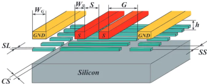
The structure of CS-CPW was presented in [9]. It is described in Fig. 1. It is composed of two central signal strips, with coplanar lateral ground strips. Thin floating ribbons (also called
SL CS WG WS S G SS Silicon h GND S S GND
Fig. 1 CS-CPW with SC-shielding structure with nomination of the dimensions.
floating shield) of width SL, separated by a gap SS, are placed below, as in a classical S-CPW.
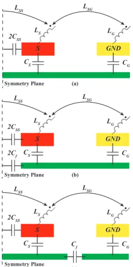
The structure of the proposed electrical model for CS-CPW is given in Fig. 2. As for S-CPWs, the electric field is confined between the CPW strips and the floating shield. The electric field is captured by the floating ribbons, instead of going directly from the central strips to the ground (as in CPW), which leads to new capacitors in the electrical model (𝐶+ and 𝐶, as
shown in Fig. 2) that are not present in microstrip or CPW structures. In practical cases, the direct capacitance between central and ground strips is negligible, because the gap 𝐺 is usually larger than the distance between signal/GND strips to the floating ribbons, ℎ. Hence, the electrical field between ground and signal strips is almost entirely captured by the floating ribbons. Meanwhile, the magnetic field is almost unperturbed by the floating shield, since it passes through it, in between the floating ribbons. Hence the inductance of S-CPW and CS-CPW is almost the same as classical single or coupled CPWs. The magnetic flux created by currents in each metal strip leads to four partial inductances, the partial self-inductance of the signal, 𝐿0, and ground strips, 𝐿1, and the partial
mutual-inductance between signal strips, 𝐿00, and between ground and
signal strips, 𝐿10. These inductances are almost equal to the
ones of a coupled CPW, due to the low perturbation of the magnetic field.
In addition to the classical structure, authors in [9] also presented two alternative topologies for added design flexibility. These topologies can include either a cut in the center of the shielding, namely Central-Cut (CC-shielding) or Side-Cut (SC-shielding).
The topologies of the lossless electrical model of the three CS-CPW architectures are shown in Fig. 2a, 2b, and 2c for the uncut, CC-shielding and SC-shielding topologies, respectively. In these models, the partial self-inductance of the ribbons is neglected as it has a very low impact unless 𝐺 becomes long enough to support any perceptible propagation, which usually means 𝐺 > 100 µm for the mm-wave band [13].
Using the described lossless model for CS-CPWs, the magnetic (𝑘6) and electric (𝑘7) coupling coefficients can be
derived, along with the even- and odd-mode characteristic impedances, 𝑍9:9; and 𝑍<==, respectively, which can be
expressed as:
𝑍<==/9:9;= ?
6@AA/BCBD
7@AA/BCBD. (1)
with 𝐿9:9;/𝐶9:9; and 𝐿<==/𝐶<== the even- and odd-mode
inductances/capacitances.
A. Magnetic coupling
The expression of 𝑘6 is independent of the chosen
architecture (i.e. uncut, CC-shielding or SC-shielding) as the shielding has a negligible impact on the magnetic flux. Coefficient 𝑘6 can be expressed as:
𝑘6=66BCBDF6@AA
BCBDG6@AA=
6HH
6HG6IF$6HI (2)
𝐿9:9; can be calculated placing a magnetic wall (i.e.
open-circuit) in the symmetry plane in Fig. 2, leading to 𝐿9:9; = 𝐿0+
𝐿1− 2𝐿01+ 𝐿00. On the other hand, 𝐿<== is calculated placing
an electric wall (i.e. short-circuit) in the symmetry plane in Fig. 2, leading to 𝐿<=== 𝐿0+ 𝐿1− 2𝐿01− 𝐿00.
B. Electric coupling for uncut CS-CPWs
The electric coupling, 𝑘7, can be calculated using the same
boundary conditions employed above for the modal analysis of 𝑘6, as:
𝑘7 =77BCBDF7@AA
BCBDG7@AA, (3)
In the case of an uncut CS-CPW, 𝐶9:9; and 𝐶<== can be
calculated as:
𝐶9:9;=77H7I
HG7I, (4)
𝐶<=== 2𝐶00+ 𝐶0. (5)
Next, in sections II.C and II.D, the analysis of the impact on 𝑘7 for CS-CPWs with either a CC-shielding or a SC-shielding
is carried out. The goal is to demonstrate how these design alternatives add a degree of freedom for the designer to modulate 𝑘7 and 𝑍<==/9:9; without altering 𝑘6.
C. Electric coupling for CS-CPWs with CC-shielding
In the case of CS-CPWs with CC-shielding, a cut is performed in the center of the ribbons as shown in Fig. 2b. This creates a
2Cf CS CG S GND LS LG LSG LSS 2CSS 2CSS 2CSS CS CG S GND LS LG LSG LSS Symmetry Plane Symmetry Plane Cf CS CG S GND LS LG LSG LSS Symmetry Plane (a) (b) (c)
Fig. 2 Elementary cell of the electrical model of a lossless CS-CPW. (a) Uncut CS-CPW. (b) CS-CPW with CC-shielding. (c) CS-CPW with SC-shielding.
capacitance, 𝐶M, between the ribbon in the left and right parts of
the symmetry plane. In this case the even-mode capacitance is not modified as compared to the uncut case and can be calculated using equation (4).
On the contrary, the new odd-mode capacitance is calculated as:
𝐶<=== 2𝐶00+
7+($7OG7I)
7HG$7OG7I. (6)
It is trivial to show that in (6), as compared to (5), the term 𝐶0 has been substituted by the equivalent capacitance of 𝐶0 in
series with 2𝐶M+ 𝐶1. Hence, the value of 𝐶<== in a CS-CPW
with CC-shielding is decreased, yielding to a reduced 𝑘7 and a
greater odd-mode characteristic impedance. However, as 𝐶9:9;
and 𝑘6 are unmodified, the even-mode characteristic impedance
remains the same as that of the uncut CS-CPW.
D. Electric coupling for CS-CPWs with SC-shielding.
For a CS-CPW with SC-shielding, the cuts in the ribbons are performed on the sides, as shown in Fig. 2c, creating a capacitance 𝐶M between the two sides of the ribbon. In this case,
the odd-mode capacitance is unmodified as compared to the uncut case and can be calculated using equation (5).
On the contrary, for this configuration, the new 𝐶9:9; is
calculated as:
𝐶9:9;=
7H7O7I
(7H7I)GQ7H7ORGQ7O7IR. (7)
In the case of the CS-shielding, the even-mode capacitance is reduced as compared to the uncut case. For the latter, 𝐶9:9;
is calculated as the series configuration of 𝐶0 and 𝐶1, as shown
in (4), whereas for CS-shielding, 𝐶9:9; is the equivalent
capacitance of the series configuration of 𝐶0, 𝐶M and 𝐶1. Hence,
(7) leads to a lower value than (4). As a result, the CS-shielded CS-CPWs presents a lower even-mode capacitance, and a greater 𝑘7 and 𝑍9:9;. The odd-mode characteristic remains the
same as that of the uncut case.
To summarize, the previous analysis shows that, for a given lateral dimension of the CS-CPW (i.e. given 𝑊0, 𝑆, 𝐺, and 𝑊1),
the different shielding topologies allow to tune 𝑘7, 𝑍9:9; and
𝑍<== independently from 𝑘6. The obtained expressions for the
magnetic coupling coefficient, 𝐶9:9; and 𝐶<==, for the three
considered shielding topologies are summarized in Table I.
Note that for any of the shielding topologies, 𝐶<== always
presents a greater magnitude than 𝐶9:9;. Hence, a comparison
on 𝑘6, 𝑘7, 𝐶9:9;, 𝐶<==, 𝑍9:9; and 𝑍<== can be carried out, as
compared to the uncut case. This comparison presented in Table II, where the symbol → stands for an unchanged parameter, ↗ stands for an increase of the parameter and ↘ represents a decrease in the parameter, as compared to the uncut case.
III. ANALYTICAL APPROACH FOR THE CALCULATION OF MODEL PARAMETERS
In this section, all the parameters of the model proposed in section II are calculated analytically, and then compared to the parameters calculated by using a quasi-static 3D solver (ANSYS Maxwell).
In the previous section, a lossless model for CS-CPWs was considered for each shielding topology. Using this model, thanks to the simple calculations that have to be performed, charts for the design goals (i.e. 𝑘7, 𝑘6, 𝑍9:9; and 𝑍<==) can be
generated for a given technology and a wide variation in the dimensions of the CS-CPW. Subsequently, designers can use these charts to get a first approximation of the necessary dimensions, but of course the losses cannot be evaluated with the previous model. Hence, even if these charts can narrow
TABLE I
SUMMARY OF THE 𝑘6,𝐶9:9; AND 𝐶<== EXPRESSIONS
Shield Uncut CC SC 𝑘6 𝐿00 𝐿0+ 𝐿1− 2𝐿01 𝐶9:9; 𝐶0𝐶1 𝐶0+ 𝐶1 𝐶0𝐶1 𝐶0+ 𝐶1 𝐶0𝐶M𝐶1 (𝐶0𝐶1) + Q𝐶0𝐶MR + Q𝐶M𝐶1R 𝐶<== 2𝐶00+ 𝐶0 2𝐶00+ 𝐶𝑠(2𝐶M+ 𝐶1) 𝐶0+ 2𝐶M+ 𝐶1 2𝐶00+ 𝐶0 CS CG S GND LSG LSS Rf Rf Rf,1 Rf,2 Rs+jωLS RG+jωLG Rs+jωLS RG+jωLG Rs+jωLS RG+jωLG Symmetry Plane Symmetry Plane Cf CS CG S GND S LSG LSS Symmetry Plane (a) (b) (c) 2Cf CS CG S GND S LSG LSS 2CSS 2CSS 2CSS
Fig. 3 Elementary cell of the electrical model of a lossy CS-CPW. Signal and Ground resistances have been merged together with Signal and Ground
partial self-inductances. (a) Uncut CS-CPW. (b) CS-CPW with CC-shielding. (c) CS-CPW with SC-CC-shielding.
TABLE II
SUMMARY OF THE 𝑘6,𝐶9:9;,𝐶<==,𝑘7,𝑍9:9; AND 𝑍<== BEHAVIOR FOR THE
CC- AND SC-SHIELD TOPOLOGIES
Shield 𝑘6 𝐶9:9; 𝐶<== |𝑘7| 𝑍9:9; 𝑍<==
CC → → ↘ ↘ → ↗
down the space of possible dimensions of the CS-CPW for a given target specification, the design of state-of-the-art CS-CPWs still requires a number of iterations in an optimization process to minimize the losses. This issue can be addressed using two approaches: (i) using time-consuming full-wave 3D EM simulations or (ii) using an electrical model considering lossy CS-CPWs.
The required time for full-wave 3D EM simulations of these structures is very long. For instance, using commercial software such as ANSYS HFSS the processing time can go from few minutes to 8-10 hours, depending on the architecture (i.e. uncut, CC-shielding or SC-shielding) and the computing power. Indeed, long design and optimization times are one of the main obstacles for the adoption of the CS-CPW structures. In order to overcome this issue, in this work we propose a complete electrical model considering lossy CS-CPW. The proposed model is conceptually depicted in Fig. 3 for each of the shielding topologies. It is based on the topology of the RLRC model proposed in [3]. It is important to remember here that the classical RLCG model is not adequate for S-CPW. In CS-CPWs, as for S-CS-CPWs, the resistance of the shielding strips, 𝑅M
(or 𝑅M,# and 𝑅M,$ for the SC-shielding case), is in series with the
shunt capacitance, the losses in the dielectric (SiO2) being
negligible as compared to metallic losses, thus leading to an RLRC model structure. The modeling approach for each element of the model for lossy CS-CPWs is based on the principle presented in [4] for S-CPW modelling. A quasi-TEM mode is considered, which allows the study of electric and magnetic fields separately. However, in this paper, a more in-depth treatment is carried out for the calculation of the inductances and resistances, considering the frequency
dependence linked to the skin effect as well as the proximity effects, which must absolutely be considered within the framework of coupled lines.
A. Capacitance calculation
Capacitance calculation for S-CPWs and their analytical expressions are thoroughly discussed in [4]. In [4], authors divide the electrical field around the strips into four regions leading to the calculus of four independent capacitances, namely bottom plate (leading to 𝐶\]^_9 capacitance), angle point
charge (𝐶^;,]9), fringe (𝐶M`a;,9) and upper plate (𝐶b\), as
depicted in Fig. 4a. The work presented in [4] also details the methodology to accurately calculate the different capacitances in these regions. The same methodology is used herein to calculate the capacitances of the CS-CPW.
Even though the scenario of signal to ground electrical coupling in an S-CPW context was discussed in [4], the case of a very close strip configuration was not considered because it does not correspond to an interesting practical case. However, for CS-CPWs, signal strips can be placed in a very close configuration to achieve greater electromagnetic coupling. Closer investigation of [4] revealed that for geometries where
0
$< ℎ0 (i.e. strips in a very close configuration) insufficient
accuracy was achieved. In that paper, the parallel plate capacitance between ground/signal strips and the floating shielding, 𝐶\]^_9, is considered to be constantly calculated as:
𝐶\]^_9= εe𝜀`]·hi
j, (8)
where 𝜀e is the vacuum dielectric constant, 𝜀` is the relative
dielectric constant between the ground/signal strips, 𝑙 is the length of the unit cell and 𝑊 is the width of the ground/signal conductor.
However, if circular paths are defined for the fringing regions as proposed in [4], when 0
$< ℎ0, some electric field is shared
beneath the conductor strips in between them. This effect is illustrated in Fig. 4b. In this scenario, 𝐶=<l; is calculated using
the formula for fringing capacitance introduced in [4] for an effective width of the conductor 𝑊0m, where:
𝑊0m= ℎ0− 𝑆/2 (9)
Note that this leads to a reduction of the effective surface of the parallel plate as defined in equation (8), which is now calculated as: 𝐶\]^_9m = εe𝜀` ]·(hHFhHn) ij ∀ 𝑊0≥ 𝑊0 m 𝐶\]^_9m = 0 ∀ 𝑊0< 𝑊0m (10) These improvements lead to a more accurate calculation of 𝐶0
and 𝐶00, showing good agreement with simulations carried out
with a commercial quasi-static simulator (i.e. ANSYS Maxwell 3D).
Finally, the capacitance between parts of the floating ribbons (𝐶M), in the case of a CC- or SC-shielding, was not discussed in
[4]. However, these capacitances can easily be calculated using the same approach used to calculate the capacitances between strips.
B. Resistance and inductance calculation
This paper aims to present a distributed electrical model and an analytical procedure to determine the lumped elements of the model that is compatible with very high frequencies (i.e. full
S1 Symmetry Plane S2 WS-WS’ WS hS tS S Ribbons Cdown Cplate’ WS’ Ribbons Cplate Cangle Ribbons Cfringe Cup (a) (b) Conductor
Fig. 4 (a) Capacitance regions of a S-CPW conductor defined as in [4]. (b) New electric field distribution, as compared to [4], for very close signal conductors. Even though other capacitance regions exist, only the modified
mm-wave and sub-THz bands). For this reason, accurate modelling of the partial mutual- and self-inductances and resistances is required across a wide frequency range.
As opposed to capacitances, which present low variation across the frequency spectrum, inductances and resistances have a strongly frequency-related behavior, the skin effect being one of the most obvious cause of this relationship. For this reason, in this article, a thorough treatment is given to the calculation of the magnitudes of inductances and resistances versus frequency.
Several approaches for accurate inductance calculation have been reported in the literature. In this work, we use a similar approach to that described in [11]. The work in [11] presents a technique for inductance calculations using a pair of rectangular conductors, although it may be extended for any conductor shape or number. The technique is based on a discretization of the conductors into a mesh of 𝑁 elements, as shown in Fig. 5. Based on a quasi-static analysis, the proposed methodology gives the resistance, and the mutual- and self-inductances as a function of the partial resistance, mutual- and self-inductances for each sub-element.
In the field of CPWs with a patterned shield underneath, the approach given in [11] has already been used in [14]. However, in [14], authors only used an unidimensional meshing (i.e. meshing along the width of the patterned CPW). This approach is sufficiently precise only for conductors whose height is very small compared to the skin depth, which is not the case here, since the goal of the present work is to provide an accurate methodology up to very high frequencies. For this reason, a two-dimensional mesh as depicted in Fig. 5a is needed.
1) Mesh definition
Following the methodology presented in [11], the faces of each conductor with an elementary length 𝛿𝑙 = 𝑆𝑆 + 𝑆𝐿,which corresponds to a period of the CS-CPW, was meshed using 𝑛$
elements with rectangular shapes (𝑛 elements in the x- and y-direction, respectively). Note that any other mesh that results in the same number of elements for the signal and ground conductors can be used without loss of generality. Considering a symmetrical CS-CPW, this leads to ground (signal) conductors with elements of the mesh having a height of 𝛿𝑦1
(𝛿𝑦0) and a width of 𝛿𝑥1 (𝛿𝑥0), respectively. Using this mesh,
𝛿𝑥0/1 and 𝛿𝑦0/1 can be defined as:
𝛿𝑥0/1= 𝑊0/1⁄𝑛
𝛿𝑦0/1= 𝑡0⁄𝑛 (11)
2) Impedance matrix definition
After defining the mesh, the next step is to define the impedance matrix. In the context of a CS-CPW, this impedance
matrix contains contributions from four conductors (strips): the two signal strips and the two ground strips.
It is important to note that the voltage is considered to be constant across the face of each conductor (i.e. in the x- and y-directions), resulting in the absence of propagation across the conductors’ face, which is realistic considering the practical dimensions. Hence, by considering the general definition of the Z-matrix, 𝒁, as a function of the voltage vector, 𝑽, and the current vector, 𝑰, in each conductor, the impedance matrix can be defined as: 𝑽 = 𝒁𝑰 (12) { 𝑉1}~ 𝑉0# 𝑉0$ 𝑉1}~ • = ⎣ ⎢ ⎢ ⎢ ⎡ 𝑍1}~ 𝑗𝜔𝑀0#1}~ 𝑗𝜔𝑀1}~0# 𝑍0# 𝑗𝜔𝑀0$1}~ 𝑗𝜔𝑀1}~1}~ 𝑗𝜔𝑀0$0# 𝑗𝜔𝑀1}~0# 𝑗𝜔𝑀1}~0$ 𝑗𝜔𝑀0#0$ 𝑗𝜔𝑀1}~1}~ 𝑗𝜔𝑀0#1}~ 𝑍0$ 𝑗𝜔𝑀1}~0$ 𝑗𝜔𝑀0$1}~ 𝑍1}~ ⎦ ⎥ ⎥ ⎥ ⎤ · · { 𝐼1}~ 𝐼0# 𝐼0$ 𝐼1}~ •, (13) where 𝜔 is the angular frequency, 𝑉a and 𝐼a are the voltages and
currents on the face of the 𝑖-th conductor, respectively, 𝑍a
represents the impedance of the 𝑖-th conductor and 𝑗𝜔𝑀‹a
represents the impedance of the partial mutual-inductance between the 𝑖-th and 𝑗-th conductors, 𝑀‹a.
At this point, 𝒁 and 𝑰 are unknown matrixes since 𝑗𝜔𝑀‹a and
𝑍a= 𝑅a+ 𝑗𝜔𝐿a, where 𝑅a and 𝐿a are the series resistance and
partial self-inductance of the 𝑖-th conductor, respectively, are frequency-dependent impedances.
Next, each diagonal element of the 𝒁 matrix, 𝒁𝒊, is calculated
using a quasi-static analysis of the elements of the mesh that define it. By assuming that the voltage across the faces of a given conductor is the same for all the elements, an equivalent circuit as depicted in Fig. 5b can be defined, hence, defining 𝑍a
as: 𝒁𝒊= • 𝑅#,#+ 𝑗𝜔𝐿#,# ⋯ 𝑗𝜔𝑀;,;#,# ⋮ ⋱ ⋮ 𝑗𝜔𝑀#,#;,; ⋯ 𝑅;,;+ 𝑗𝜔𝐿;,; ‘, (14) where 𝑅’,“ and 𝐿’,“ are the DC-resistance and DC-partial
self-inductance of the element in the 𝑘-th row and the 𝑚-th column of the mesh. 𝑀<,\’,“ is the quasi-static value of the mutual
inductance between the elements in the 𝑘-th row and the 𝑚-th column and in the 𝑜-th row and the 𝑝-th column, respectively. The DC-resistance is classically calculated as:
Symmetry Plane
Signal Conductor GND Conductor
S21,1 S2n,n S2n,1 S21,n S21,2 S22,1 ... ... ... ... ... ...... ... G21,1 G2n,n G2n,1 G21,n G21,2 G22,1 ... ... ... ... ... ...... ... G δyG δxG WG WS δxS δyS tS S/2 (a) R1,1(δx,δy) L1,1(δx,δy) R1,2(δx,δy) L1,2(δx,δy) Rn,n(δx,δy) Ln,n(δx,δy) V(z+δl) V(z) I1,1 I1,2 In,n M1,1(δx,δy) 1,2 M1,2(δx,δy) n,n M1,1(δx,δy) n,n (b) z y x
𝑅~7=—·˜™·˜š] . (15)
The value of the partial self- and mutual-inductance can be calculated using equations (8) and (9) in [12], respectively. Finally, the elements outside the diagonal of 𝒁, 𝑗𝜔𝑴𝒋𝒊, are in
their turn 𝑛$∙ 𝑛$ square matrixes containing the partial mutual
inductances between the elements of the 𝑖-th and 𝑗-th conductors.
At this point, all the scalars in 𝒁 can be substituted by their matrixes, obtained through the previous analysis, leading to 𝒁𝒎,
a 4𝑛$∙ 4𝑛$ square matrix. 𝑽 𝒊
𝒎 is the column matrix containing
the voltage at the face of each mesh element in the conductor 𝑖. Hence, in the absence of propagation across the face of the conductor, 𝑽𝒊𝒎 is a column vector with a single value. On the
other hand, 𝑰𝒊𝒎 is redefined as a column vector containing the
currents flowing through each element of the 𝑖-th conductor, which are unknown and different, as depicted in Fig. 5b.
3) Admittance matrix derivation
The next step is to define the meshed admittance matrix, 𝒀𝒎,
as follows: 𝑰𝒎= 𝒀𝒎· 𝑽𝒎 ⎣ ⎢ ⎢ ⎡𝑰𝑮𝑵𝑫𝒎 𝑰𝑺𝟏𝒎 𝑰𝑺𝟐𝒎 𝑰𝑮𝑵𝑫𝒎 ⎦ ⎥ ⎥ ⎤ = ⎣ ⎢ ⎢ ⎡𝒀𝟏𝟏𝒎 𝒀𝟏𝟐𝒎 𝒀𝟐𝟏𝒎 𝒀𝟐𝟐𝒎 𝒀𝟏𝟑𝒎 𝒀𝟏𝟒𝒎 𝒀𝟐𝟑𝒎 𝒀𝟐𝟒𝒎 𝒀𝟑𝟏𝒎 𝒀𝟑𝟐𝒎 𝒀𝟒𝟏𝒎 𝒀𝟒𝟐𝒎 𝒀𝟑𝟑𝒎 𝒀𝟑𝟒𝒎 𝒀𝟒𝟑𝒎 𝒀𝟒𝟒𝒎⎦ ⎥ ⎥ ⎤ · ⎣ ⎢ ⎢ ⎡𝑽𝑮𝑵𝑫𝒎 𝑽𝑺𝟏𝒎 𝑽𝑺𝟐𝒎 𝑽𝑮𝑵𝑫𝒎 ⎦ ⎥ ⎥ ⎤ (16) where 𝒀𝒎= (𝒁𝒎)F#.
Then, the equivalent admittance of each conductor can be calculated as:
𝑌a‹= ∑ ∑ 𝒀; ; 𝒊𝒋𝒎 (17)
Next, the scalar values obtained in (17) can be introduced in (16), leading to the admittance matrix:
{ 𝐼1}~ 𝐼0# 𝐼0$ 𝐼1}~ • = { 𝑌## 𝑌#$ 𝑌$# 𝑌$$ 𝑌#« 𝑌#¬ 𝑌$« 𝑌$¬ 𝑌«# 𝑌«$ 𝑌¬# 𝑌¬$ 𝑌«« 𝑌«¬ 𝑌¬« 𝑌¬¬ • · { 𝑉1}~ 𝑉0# 𝑉0$ 𝑉1}~ •, (18)
4) Reduction of the matrix dimension
Both ground strips are assumed to be connected at the same voltage. Hence, a reduced admittance matrix, 𝒀𝒓,can be defined
as: ® 𝐼0# 𝐼0$ 2𝐼1}~ ¯ = ® 𝑌𝑌$$«$ 𝑌𝑌$««« 𝑌𝑌$#«#+ 𝑌+ 𝑌$¬«¬ 𝑌#$+ 𝑌¬$ 𝑌#«+ 𝑌¬« 𝑌##+ 𝑌#¬+ 𝑌¬#+ 𝑌¬¬ ¯ °±±±±±±±±±±±±±±²±±±±±±±±±±±±±±³ · 𝒀𝒓 ®𝑉𝑉0#0$ 𝑉1}~ ¯ (19) Finally, the reduced impedance matrix 𝒁𝒓 can be calculated
as 𝒁𝒓= (𝒀𝒓)F#, leading to: ® 𝑉𝑉0#0$ 𝑉1}~ ¯ = { 𝑍0# 𝑗𝜔𝑀0$0# 𝑗𝜔𝑀1}~,\0# 𝑗𝜔𝑀0#0$ 𝑍 0$ 𝑗𝜔𝑀1}~,\0$ 𝑗𝜔𝑀0#1}~,\ 𝑗𝜔𝑀0$1}~,\ 𝑍1}~,\ • °±±±±±±±±±±±²±±±±±±±±±±±³𝒁 𝒓 ® 𝐼𝐼0#0$ 2𝐼1}~ ¯ (20) where 𝑍a is a complex value of the form 𝑅a+ 𝑗𝜔𝐿a, where 𝑅a
and 𝐿a are the resistance and partial self-inductance of the 𝑖-th
conductor, respectively. 𝑀‹a is the partial mutual-inductance
between conductors 𝑖 and 𝑗.
Note that after all these calculations, the resistances, partial self- and mutual-inductances now take into account the frequency effects (e.g., skin effect) and proximity effects, as explained in [11].
5) Calculation of reduced model parameters
The reduction of the matrix leads directly to a simplification of the model, that can be represented as the distributed model as shown in Fig. 6, for each CS-CPW configuration (uncut shielding, and CC- or SC-shielding).
The value of the model parameters is calculated as follows. The capacitors are calculated using the methodology presented in [4] together with the new developments considered in section III.A. The signal and ground strips resistance (𝑅0/1) is
CS LSG LSS Rf /2 Rs+jωLS RG+jωLG CS G Rs+jωLS LSG 2CG CSS δl (a) CS LSG LSS Rf Rs+jωLS RG+jωLG CS G Rs+jωLS LSG CG Cf CG Rf CSS δl (b) CS LSG LSS Rf /2 Rs+jωLS RG+jωLG CS G Rs+jωLS LSG 2CG 2Cf CSS δl (c)
Fig. 6 Reduced distributed model of a CS-CPW with an elementary length of 𝛿𝑙 with (a) uncut floating ribbons, (b) CC-shield and (c) SC-shield.
calculated as ℜ(𝑍0/1), the signal and ground partial
self-inductance (𝐿0/1) is calculated as ℑ(𝑍0/1)/𝜔 in (20). Finally,
the partial mutual-inductance between signal or ground strips (𝐿00/01) is calculated as ℑ(𝑗𝜔𝑀0/1,\0 )/𝜔 in (20).
Finally, the resistance of the floating ribbons 𝑅M is calculated
using (15). It is interesting to notice that since the floating ribbons are implemented using very thin strips (due to the characteristics of the BEOL stack of our BiCMOS technology), the resistance of the floating ribbons is practically constant in the frequency band of interest. However, for higher frequencies or thicker floating ribbons, the procedure described above for resistance and inductance calculation may be used without loss of generality. The same reasoning is valid for losses linked to eddy currents in the floating ribbons.
IV. VERSATILITY OF CS-CPWS
As previously introduced in section II, using the model described in the previous section together with equations (1) to (7), the designer can make a quick exploration of the design space of CS-CPWs in a given technology for performance optimization.
To illustrate this point as well as the possibilities offered by CS-CPWs in a given technology, some variations of the geometry of a CS-CPW were performed on the 8-metal STM
55-nm BiCMOS technology.
This technology features a Back-End-Of-Line (BEOL) with an ultra-thick top metal, two thick metals below (i.e. metals 6
and 7) and 5 thin metals. In this study, a stack composed of metal 7 and metal 8 was used for the signal and ground strips.
The floating shield was placed on metal 5, leading to an ℎ of around 2 µm. In this context, 𝑆 and 𝑊1 were fixed to 2 and 15
µm, respectively. 𝑆𝑆 and 𝑆𝐿 were fixed to 0.5 µm. Finally, for the SC- and CC-shielded structures, 𝐶𝑆 was fixed to 2 µm.
As a case-study example, in this configuration, we varied the ratios 𝐺/𝑆 and 𝑊0/ℎ in the ranges from 10 to 70 and 1 to 13,
respectively. The operation frequency was set to 100 GHz. The derived |𝑘7| and 𝑍7 are plotted in Fig. 7a and 7b, respectively.
𝑍7 is calculated as:
𝑍7= ¶𝑍9:9;· 𝑍<==. (21)
In Fig. 7, the three architectures of the floating shield were considered, i.e. uncut, SC- and CC-shielding.
Fig. 9 presents |𝑘6| calculated for the same dimension ratios.
The same values of |𝑘6| are found for all the shielding
architectures, since as it was discussed above, the shielding has a negligible effect on the magnetic coupling coefficient.
Some simple design rules can be extracted from the charts in Figs. 7 and 9. First, the electric coupling does not depend on the variation of 𝐺 as long as this dimension is large enough to prevent a direct coupling between the signal and ground strips (which is the case for our study). Second, the electric coupling decreases with 𝑊0 for the CC-shielding case. This can easily be
explained by the fact that 𝐶9:9; increases more rapidly than
𝐶<==, the value of the latter being dominated by 2𝐶00. On the
other hand, for the uncut and SC-shielding cases, the electric coupling coefficient first decreases and then increases with 𝑊0/ℎ. This is especially remarkable for the SC-shielding case.
For the uncut shielding, this can be explained by the fact that for a very narrow strip (i.e. small 𝑊0/ℎ ratio), the value of the
even-mode capacitance is almost 𝐶0. When the value of 𝐶0 starts
increasing with 𝑊0/ℎ, 𝐶9:9; increases more rapidly than 𝐶<==,
leading to a decrease of |𝑘7|. However, if 𝑊0/ℎ further
increases, the value of 𝐶9:9; is rapidly limited by the value of
𝐶1, while 𝐶<== continues to increase, leading to an increase of
|𝑘7|. A similar reasoning can be followed to analyze the
behavior of |𝑘7| for the SC-shielding case. In this case, 𝐶1 is in 0 5 WS/h 20 30 40 20 50 Zc ( ) 60 10 70 80 40 G/S 60 0 5 WS/h 0.4 0.45 0.5 0.55 20 0.6 0.65 kC 0.7 10 0.75 0.8 40 G/S 60 || Ω SC CC no Cut (a) (b)
Fig. 7 (a) Characteristic impedance of a CS-CPW for the uncut, SC- and CC-shielding. (b) |𝑘7| of a CS-CPW for the uncut, SC- and CC-floating shield.
𝑆=2µm, 𝑊1=15 µm, 𝑆𝑆=𝑆𝐿=0.5 µm, and 𝐶𝑆=2 µm. 0 5 WS/h 10 0.3 0.4 10 G/S 20 0.5 kL 30 40 0.6 15 50 60 0.7 70 ||
Fig. 9 |𝑘6| of a CS-CPW for the uncut, SC- and CC-floating shield. 𝑆=2µm,
𝑊1=15 µm, 𝑆𝑆=𝑆𝐿=0.5 µm, and 𝐶𝑆=2 µm.
Metal 7
Metal 6
Metals 1 to 5
Silicon
Metal 8
Alucap
series with 𝐶M, making the change in the slope of |𝑘7| happen
for smaller values of 𝑊0/ℎ.
The behavior of the magnetic coupling coefficient can be analyzed in the same way. When 𝐺/𝑆 increases, the partial self-inductance of the signal strips (𝐿0) increases because the
magnetic flux increases, and the partial-mutual inductance between signal and ground strips (𝐿10) decreases due to the
increased distance between those strips. On the other hand, the signal-to-signal partial mutual-inductance (𝐿00) does not
change according to 𝐺/𝑆 ratio. Based on these considerations, from equation (1) it can be derived that an increase of 𝐺/𝑆 leads to a decrease of |𝑘6|. On the other hand, the increase of 𝑊0/ℎ
also leads to a decrease of the magnetic coupling coefficient. This can be easily explained by the fact that the signal-to-signal partial-mutual inductance decreases more rapidly than 𝐿0, while
𝐿1 and 𝐿10 are practically unmodified by the variation of 𝑊0/ℎ.
Hence this leads to a decrease of |𝑘6| with 𝑊0/ℎ.
Finally, the charts in Figs. 7 and 9 show that it is possible to vary independently 𝑘· and 𝑘], for a given value of 𝑍·.
In the next section, in order to make a proof-of-concept of the CS-CPW technology and to validate the modelling approach and derived design charts, mm-wave couplers are designed and characterized.
V. APPLICATION TO MM-WAVE COUPLERS
As a direct application of the described design methodology, we present in detail the design procedure, practical
implementation considerations and experimental
characterization for two different backward directional couplers. The first case study is a coupler designed for a 3-dB coupling at 120 GHz. 3-dB coupling is a challenge when dealing with advanced CMOS/BiCMOS technologies, since the distance between coupled strips is limited by the technology design rules. For instance, the minimum distance between strips in the BiCMOS 55-nm technology for strips wider than 10 µm is 5 µm. As presented in [9], such a distance leads to a maximum coupling of 11 dB when considering classical coupled microstrip lines. As explained in the introduction, some authors developed broadside coupling in order to address this issue, which leads to complex design methodologies as compared to that proposed in the present paper, from the moment we have an electric model like the one developed here. The second case study is also a 3-dB coupler, but at a much higher frequency, around 180 GHz, in order to show the capability of CS-CPWs to work at high frequency. To give further insight into the feasibility and performance of the proposed design methodology, we present a direct comparison between the measurement results, the proposed analytical model and 3D EM simulations carried out with ANSYS HFSS.
A. Design Procedure
A 3-dB coupler corresponds to a coupling coefficient 𝑘 equal to 1/√2, i.e. about 0.7. According to the port numbering used in this article, the coupling coefficient corresponds to |𝑆«#|,
considering the third port to be the coupled one. In terms of 𝑘7
and 𝑘6, the coupling coefficient is calculated as follows:
𝑘 =?¹ º»¼½ º¾¼½¿¹º¾¼Àº»¼À¿F# ?¹º»¼½º¾¼½¿¹º¾¼À º»¼À¿G# (22) However, 𝑘 only defines the amount of energy transmitted from the input to the coupled output. In order to get high directivity, the condition of equal electric and magnetic coupling coefficients must be respected:
𝑘7= 𝑘6=√$# ≈ 0.7 (23)
Similar charts to the ones presented in the previous section were used to explore the space of dimensions that verifies the condition in equation (23).
Once the space of possible dimensions was narrowed down to a few possibilities, a model-based optimization was performed to obtain the dimensions that gave the best performance. Finally, model-based results were validated by EM simulation with good agreement.
B. Measurement results
For the design of both couplers, metals 7 and 8 were stacked using the maximum amount of vias allowed by the design rules of the technology to obtain artificially thicker conductors for the ground and signal strips, leading to lower resistive losses and greater 𝐶00. On the other hand, the floating shield was
placed on metal 5, which is the closest layer to metals 7 and 8 featuring a thin strip. This choice was done so as to reduce the eddy currents in the floating ribbons [15] while keeping a relatively high slow-wave effect, for miniaturization purposes. Finally, as it can be retrieved from the analysis carried out in the previous section, a SC-shielding was used as it offers a greater range of lateral dimensions complying to the design condition in (23).
1) 3-dB Coupler at 120 GHz
The 3-dB coupler with a central frequency of 120 GHz was TABLE III
DIMENSIONS OF THE 120-GHZ 3-DBCOUPLER
𝑊0
(µm) (µm) 𝑆 (µm) 𝐺 (µm) 𝑊1 𝑆𝑆 = 𝑆𝐿 (µm) (µm) 𝐶𝑆
2 1.8 20 15 0.5 2
Reference planes
after TRL calibration
Fig. 10 Microphotograph of the 120-GHz 3-dB coupler and the reference planes after multimode TRL calibration.
designed using the above considerations, a length of 255 µm and the dimensions given in Table III.
The fabricated device, whose microphotograph is shown in Fig. 10, was measured using an Anritsu VectorStar ME7838A4 4-ports Vector Network Analyzer (VNA), from 1 GHz to 145 GHz. A first-tier LRRM (Line-Reflect-Reflect-Match) calibration [16] was performed on a commercial ISS (Impedance Standard Substrate) to set the reference planes at the probe tips. Subsequently, as a second-tier calibration, an on-wafer multimode TRL calibration [17] was performed in order to set the reference planes at the input/output of the coupler, as shown in Fig. 10.
In a TRL calibration, the Line standard sets the impedance for which the system is calibrated. For an accurate read-out of this impedance, it is necessary that the electrical length difference between the Line and Thru standards is significant (i.e. some degrees) to ensure a proper reading. On the other hand, the electrical length difference has to be sufficiently short to avoid approaching 𝜋, where resonances appear. As a rule-of-thumb, for the frequencies where the electrical length difference between the Line and Thru standards is between 10º and 170º, it can be considered that the system is accurately calibrated. In this work, the Line and Thru standards lengths were set to 850 µm and 300 µm, respectively. This leads to an electrical length between Line and Thru standards equal to 90º at 85 GHz.
Hence, calibration is accurate in the 10-145 GHz band. The width of the strips was set to 7.7 µm and their spacing to 2 µm, leading to an even- and odd-mode characteristic impedance equal to 75 Ω and 25 Ω, respectively. These dimensions were chosen as they allow using the same access lines for the coupler, while presenting sufficiently similar phase velocities for the Line even- and odd-modes to avoid undesired resonances in the band of interest. Hence, following (21) the S-parameters after the on-wafer TRL are calibrated to 43 Ω. A subsequent renormalization was numerically performed to obtain S-parameters referenced at a 50-Ω impedance.
Fig. 11 shows the magnitude of the S-parameters for the measurement (solid-line), analytical model (dashed-line) and 3D EM simulations (dots). Even though measurements could only be carried out up to 145 GHz, model-based and 3D EM simulation-based results are shown up to 240 GHz for comparison purposes. Note that some discontinuities are observed in the isolation (𝑆¬#) and return loss measurements
(𝑆##); they appeared after the second-tier calibration. Regarding
the measurement results, at 120 GHz the coupler shows -3.7 dB at the through port, -3.6 dB at the coupled port, a return loss and an isolation of around 30 dB. At this frequency, the analytical model predicts -3.6 dB at the through port, -3 dB at the coupled port and around 22 dB of isolation and return loss. Finally, the 3D EM simulation predicted -3.6 dB at the through port, -3.5 dB at the coupled port and around 26 dB of isolation and return loss, in a good agreement with the measurement results and the proposed analytical model.
Above 180 GHz it can be observed that the EM simulation and the model-based results diverge. This can be easily explained by a difference in the magnitude of some of the parameters in the distributed model, which make the coupler resonate at a lower frequency than the one given by EM simulation.
Fig. 12 shows the phase difference between the through port and the coupled port seen from the input (i.e. ∠𝑆«#− ∠𝑆$#), for
the measurement (solid-line), model- (dashed-line) and EM-based (dots) datasets. At 120 GHz, the phase difference between these two ports is around 94º, with almost a flat curve throughout most of the measured frequency band. The
0 50 100 150 200 Frequency (GHz) -60 -50 -40 -30 -20 -10 0 |S | ( dB ) S11 S21 S31 S41 Measure Analytical HFSS
Fig. 11 S-parameters magnitude of the 120-GHz 3-dB coupler. Measurement, analytical model, and 3D EM simulation results are represented as solid-lines,
dashed lines and dots, respectively.
0 50 100 150 200 Frequency (GHz) 60 70 80 90 100 110 120 S21 -S31 ( °) Measure Analytical HFSS
Fig. 12 Phase difference between the through port (i.e. port 3) and the coupled port (i.e. port 2) seen from the input (i.e. port 1) of the 120-GHz coupler. Measurement, analytical model, and 3D EM simulation results are represented as solid-lines, dashed line
0 50 100 150 200 Frequency (GHz) 0 20 40 60 80 100 120 140 160 180 200 Zc ( ) Even Odd Mixed Measure Analytical HFSS Ω
Fig. 13 Even-, odd- and mixed-mode characteristic impedances for the three considered datasets for the 120-GHz coupler. Measurement, analytical model, and 3D EM simulation results are represented as solid-lines, dashed lines and
maximum error in the measurement (as compared to ideal case of 90°) is 7°. Note that in Fig. 12, the model-based results show an overall better agreement with the measurement results, as compared to the EM-based results. Again, the resonance at the frequency for which the coupler reaches an electrical length of 𝜆1/2, where 𝜆1 is the guided electrical length, can be observed
around 230 GHz, leading to disagreement between the EM- and model-based data sets.
Finally, Fig. 13 shows the even-, odd-, and mixed-mode
characteristic impedance of the measured (solid-line), EM- (dots) and model-based (dashed-line) data sets. These characteristic impedances could be measured thanks to the use of a 4-ports VNA. To authors’ knowledge, this is the first time that such a measurement is shown at a frequency higher than 110 GHz for coupled-lines.
The agreement between measurement (solid-line), model- (dashed-line) and EM-based (dots) results is very good for the odd-mode characteristic impedance over the whole bandwidth, from DC to 145 GHz. On the contrary, the agreement for the even-mode characteristic impedance is less good, with a difference of 10 to 15% between the measurement, model- and EM-based results. Consequently, the difference on the mixed-mode impedance is of the order of 5 to 8%.
2) 3-dB Coupler at 185 GHz
Beyond demonstrating the feasibility of the proposed design methodology, our second case study has been designed with the additional goal of demonstrating the feasibility and performance of the CS-CPW structure for the upper end of the mm-wave band. For the 185-GHz coupler case study, the design methodology was similar to that used for the 120-GHz coupler. The length of the 185-GHz coupler is 140 µm, the other dimensions being given in Table IV. The same metals layers as for the 120-GHz coupler were used for the ground and signal strips as well as for the floating ribbons. Finally, a cut of 2 µm was also performed on the side of the floating ribbons, in a SC-shielding configuration.
The measurement of the 185-GHz coupler was performed with a 4-ports VNA up to 145 GHz, and with a 2-ports VNA above 145 GHz. From 1 GHz to 145 GHz, the 185-GHz coupler was measured using 4-ports setup on an Anritsu VectorStar ME7838A4 Vector Network Analyzer (VNA) with a first-tier LRRM calibration and a second-tier on-wafer multimode TRL calibration, as for the 120-GHz coupler. The microphotograph of the fabricated device used for this measurement, together with the reference planes after TRL calibration is shown in Fig. 14a.
Measurements from 140 GHz up to 220 GHz were performed as 2-ports measurements using an Oleson extender associated to a R&S VNA. For each of the measurements, a first-tier LRRM calibration was performed and a subsequent 2-ports second-tier TRL [18] calibration was carried out in order to set the reference planes at the input/output of the coupler. The 2-ports TRL was performed on a Line of length 520 µm and a Thru of length 200 µm, leading to a Thru-Line electrical length difference of 105º at 140 GHz and 165º at 220 GHz. The characteristic impedance of the Line and Thru standards was set to 50 Ω.
In order to characterize the 185-GHz coupler above 140 GHz, three circuits were fabricated, each circuit making it possible to measure two S-parameters among four. For each
TABLE IV
DIMENSIONS OF THE 185-GHZ COUPLER
𝑊0
(µm) (µm) 𝑆 (µm) 𝐺 (µm) 𝑊1 𝑆𝑆 = 𝑆𝐿 (µm) (µm) 𝐶𝑆
2 2.4 20 15 0.5 2
Reference planes after TRL calibration
(a)
Reference planes after TRL calibration
(b)
(c)
Reference planes after TRL calibration
Reference planes after TRL calibration
(d)
Fig. 14 Microphotographs of the 185-GHz coupler and the reference planes after TRL calibration for: (a) 4-ports measurement, (b) 2-ports measurement of the Thru, (c) 2-ports measurement of the coupling, and (d) 2-ports measurement of the isolation.
measurement, the two ports that are not being measured were loaded with 50-Ω on-wafer loads. Figs. 14b, 13c and 14d show the three circuits that were used to measure the S-parameters of the 185-GHz coupler at the through, coupled and isolation ports, respectively.
Fig. 15 shows the measured (solid-line), EM- (dots) and model-based (dashed-line) S-parameters of the considered coupler from 1 GHz up to 360 GHz (up to 220 GHz for measurement data). Note that, in the 140-220 GHz band, for the measurement results, three sets of |𝑆##| are plotted. These
correspond to the return loss of each of the three measurements performed in this band.
In the 1-145 GHz band, all three data sets show very good agreement. Beyond, the measurements continuity between this band and the 140-220 GHz band is not very good for the return loss and the isolation (|𝑆¬#|). This can be easily explained due
to the non-idealities of the on-wafer loads. For example, when the measurement of the isolation is performed, if the on-wafer load presents some reactive parasitic, some signal is transmitted from the input to the theoretically isolated port, similarly to the working principle of Reflection-Type Phase Shifters (RTPS). Even though these effects impact all the measured S-parameters of the coupler, those parameters whose magnitude is smaller (i.e. return loss and isolation), suffer from a greater relative deviation. This is why the three return loss curves measured on the 140-220 GHz band vary by more than 10 dB between them.
Hence, with a 4-ports measurement, where all ports are 50 Ω, better isolation and return loss can be expected. At 185 GHz, the measured, EM- and model-based results show a coupling of 3.7, 4.2 and 3.2 dB, respectively. The through port presents -2.9, -2.6 and -3.1 dB for the measurement, EM- and model-based results, respectively. The EM- and model-model-based isolation (return loss) are 20 dB (23 dB) and 37 dB (37 dB), respectively.
Next, in the 220-360 GHz band, the through and coupled S-parameters present good agreement between the analytical model and the 3D EM simulations. However, as for the previous 120-GHz coupler, the isolation and return loss between these datasets diverge when considering frequencies for which the coupler electrical length gets closer to 𝜆1/2. This
is especially remarkable above 300 GHz.
Fig. 16 displays the phase difference between the through and coupled ports seen from the input, for the measurement (solid-line), EM- (dots) and model-based (dashed-line) datasets. The agreement between measurement, EM- and model-based results is very good. At 185 GHz, the phase difference is equal to 95°, 95° and 91° for measurement, EM- and model-based results.
In Fig. 17, the odd-, even- and mixed-mode characteristic impedances are shown. As for the 120-GHz coupler, the agreement between measurement (solid-line), model- (dashed-line) and EM-based (dots) results is very good for the odd-mode characteristic impedance, from DC to 145 GHz. On the contrary, the agreement for the even-mode characteristic impedance is limited, with a difference of 10 to 15% between the measurement, EM- and model-based results. Consequently, the difference on the mixed-mode impedance is of the order of 5 to 8%.
VI. COMPARISON TO THE STATE-OF-THE-ART
To put the obtained performance figures into perspective, we present a direct comparison between our experimental measurements and state-of-the-art designs in the literature. Table V summarizes this comparison.
In [19] authors report a coupled-line coupler using the CS-CPW architecture at 90 GHz with the floating shield connected
50 100 150 200 250 300 350 Frequency (GHz) -60 -50 -40 -30 -20 -10 0 |S | ( dB ) S11 S21 S31 S41 Measure Analytical HFSS
Fig. 15 S-parameters magnitude of the 185-GHz 3-dB Coupler. Measurement is represented as solid-lines, the analytical model results are plotted using
dashed lines and the 3D EM simulation results are the depicted as dots.
50 100 150 200 250 300 350 Frequency (GHz) 60 70 80 90 100 110 120 S21 -S31 ( °) Measure Analytical HFSS
Fig. 16 Phase difference between the through port (i.e. port 3) and the coupled port (i.e. port 2) seen from the input (i.e. port 1) of the 185-GHz coupler.
0 50 100 150 200 250 300 350 Frequency (GHz) 0 20 40 60 80 100 120 140 160 180 200 Zc ( ) Even Odd Mixed Ω Measure Analytical HFSS
Fig. 17 Even-, odd- and mixed-mode characteristic impedances for the three considered datasets for the 185-GHz coupler, extracted from measured
to the ground strips (i.e. grounded). The signal lines are designed using two metal layers (i.e. one layer for each strip), which are braided along the coupler length. This approach helps to equalize the even- and odd- velocities, yielding the coupler with the greatest relative bandwidths (i.e. 1-dB and ±3º BWs) among its counterparts in the published literature. However, relatively poor return loss and magnitude imbalance are achieved. On the other hand, the miniaturization achieved by the slow-wave effect makes it the smallest among the considered couplers.
Authors in [20] report a Coupled CPW in a broadside configuration. The coupler was designed in a BenzoCycloButene (BCB) substrate over a GaAs front-end. The BCB, which is not compatible with most of the commercial CMOS and BiCMOS technologies, offers a substrate for the design of high-𝑄 passive structures. However, due to the broadside architecture the achieved return loss, isolation and relative bandwidths are quite reduced.
In [21], Semi-Lumped broadside microstrip lines are used for the design of a 3-dB coupler at 60 GHz. In this work, thanks to the use of lumped capacitors and inductors, the phase velocities are equalized. Even if succeeding in this equalization, a rapid degradation of its performance can be observed above around 70 GHz, probably due to the decrease of the 𝑄-factor of the used lumped elements.
Authors in [22] report a meandered, Complementary-Conducting-Strip Coupled Line (CCS CL). The CCS CL is a structure similar to a traditional coupled microstrip line, whose ground plane has been altered by performing openings in it. Although this approach is sufficient to ensure an even coupling between both strips, limited isolation and return loss are reported. Moreover, the openings allow the electromagnetic field to penetrate the silicon, resulting in the greatest losses of the considered couplers.
Finally, in [23], a classical 3-dB coupler is designed using microstrip coupled-lines in a broadside configuration. The relatively poor return loss and isolation, together with the reduced bandwidth, show the difficulty of equalizing the propagation constants of the even- and odd- modes over a large bandwidth using the broadside architecture.
The 120-GHz coupler presented in this paper shows the best
matching and isolation over an ultra-wideband among all the couplers considered in Table V. In addition, the 120-GHz coupler presents one of the lowest magnitude imbalances between its through and coupled ports. If a bandwidth defined at 1 dB from the maximum coupling level is considered, the 120-GHz coupler presents a bandwidth as high as 75 GHz. On the other hand, if a bandwidth at ±3º is considered regarding the central frequency, this coupler presents around 110 GHz of bandwidth.
The 185-GHz coupler, even though better results may be expected from a 4-port characterization, presents a magnitude imbalance of 0.8 dB, which is of the same order of magnitude as the coupler reported in [19]. In addition, it presents an isolation and return loss also comparable to the other couplers. To summarize, in this work two CS-CPW-based coupled-line couplers were presented, which to the best of our knowledge, report the highest central frequencies ever reported in the CMOS and BiCMOS literature. Moreover, they present better or state-of-the-art performance, with comparable sizes to other existing mm-wave couplers thanks to the use of slow-wave propagation.
VII. CONCLUSION
The work in this paper concerned the development of Coupled-Slow-wave CoPlanar Waveguide (CS-CPW) on CMOS advanced technology at mm-wave frequencies. Compared to traditional coupled CPW or microstrip lines, the CS-CPW structure exhibits a high quality factor, longitudinal miniaturization, and probably the most important from a design point of view: a flexible choice in the coupling level.
In the first part of the paper, a full parametric electrical model, derived from a physical analysis of CS-CPWs and three associated shielding topologies was proposed. It is the first electrical model allowing a full-analytical modelling of the CS-CPW structure. Next, charts were plotted in order to show the degrees of freedom of the structure thanks to its intrinsic topology and the floating shield topologies.
The proposed model was then validated using two 3-dB couplers with central frequencies of 120 GHz and 185 GHz, respectively. These couplers showed state-of-the-art or beyond state-of-the-art performance while keeping comparable sizes as TABLE V
STATE-OF-THE-ART MM-WAVE COUPLERS
Ref. This work1 This work2 [19] [20] [21] [22] [23]
Tech. 55-nm BiCMOS 55-nm BiCMOS 65-nm CMOS 35-nm GaAs BiCMOS 130-nm 180-nm CMOS BiCMOS 0.35-µm Topology CS-CPW CS-CPW CS-CPW Broadside SL-Broadside Meandered CCS CL Meandered Broadside
Frequency (GHz) 120 185 90 270 60 40 75 Through (dB) 3.7 2.9 3.5 3.9 3.9 4.5 4 Coupling (dB) 3.6 3.7 4.4 4.1 3.8 4.5 4 Return Loss (dB) >25 >15‡ >18 >13 >25 >13 >15 Isolation (dB) >25 >15 - >17 >25 >18 17*** 1-dB BW (GHz) 75 80 55 51†† 34 20 30 ±3º BW (GHz) 110 80 >60 51‡‡ 47** 10 30 Size* (𝜆$) 0.003 0.0045 0.001 0.013 0.003 0.005 -

![Fig. 4 (a) Capacitance regions of a S-CPW conductor defined as in [4]. (b) New electric field distribution, as compared to [4], for very close signal conductors](https://thumb-eu.123doks.com/thumbv2/123doknet/13384299.404890/6.918.103.407.93.465/capacitance-regions-conductor-defined-electric-distribution-compared-conductors.webp)