Design & Optimization of Automotive Power
Electronics Utilizing FITMOS MOSFET Technology
by
Wei Li
S.B., California Institute of Technology, 2007
MASSACHUSETTS INSTITUTE OF TECHNOLOGY
AUG 0
7
2009
LIBRARIES
Submitted to the Department of Electrical Engineering and Computer Science in partial fulfillment of the requirements for the degree of
Master of Science
at the
MASSACHUSETTS INSTITUTE OF TECHNOLOGY
June 2009
© Massachusetts Institute of Technology 2009. All rights reserved.
ARCHIVES
Author... ...
Department of Electrical Engineering and Computer Science May 21, 2009 C ertified by ... ...
David J. Perreault Professor, Department of Electrical Engineering and Computer Science Thesis Supervisor
Terry P. Orlando Accepted by ...
Chairman, Department Committee on Graduate Students
Design & Optimization of Automotive Power Electronics
Utilizing FITMOS MOSFET Technology
by Wei Li
Submitted to the Department of Electrical Engineering and Computer Science on May 21, 2009, in partial fulfillment of the
requirements for the degree of Master of Science
Abstract
Power electronics are essential to many automotive applications, and their importance continues to grow as more vehicle functions incorporate electronic controls. MOSFETs are key elements in automotive power electronic circuits and MOSFET characteristics can strongly affect circuit size, cost and performance. Advances in MOSFET technology are thus of great importance to the advancement of automotive electronics.
The new Floating Island and Thick Bottom Oxide Trench Gate MOSFET (FITMOS) developed at Toyota has tremendous potential for automobile applications due to its reduced on-resistance, improved temperature coefficient of resistance and reduced gate charge and input capacitance. In this research, we investigated the detailed characteristics of FITMOS devices, developed the SPICE model for simulation and explored their applications in the design of automotive power electronics. Specifically, we identified how to best utilize the FITMOS characteristics to benefit power circuit design and on quantifying the gains that can be achieved through their use. We also expose a previously unrecognized phenomenon in the FITMOS MOSFET. In particular, we show that the on-state resistance of the device depends on both frequency and on peak di/dt at a given frequency. This dynamic on resistance variation can have a significant application impact.
Thesis supervisor: David J. Perreault
Acknowledgements
First of all, I am deeply indebted to my advisor Prof.Perreault to give me this precious opportunity to explore the power electronic filed. His valuable discussion and suggestion guided me through the whole research. In addition, I also want to thank Toyota Motor Corp to support this project and my tuition.
I want to thank all my group mates, YeHui, Brandon, Robert, Dave G, Tony and Jackie. They are always willing to help and share their experience.
I also want to thank all of the staff members and my fellow students from LEES who bring the sunshine and love to the basement of the MIT dome. Especially to our assistant, Vivian, I am impressed by the amount of work she needs to handle.
In addition, I would like to thank all my friends in or outside of MIT. You guys made my life joyful. Especially to Daniel, he is knowledgeable and user-friendly. You will feel confidence to work with him.
In the end, I want to thank my parents and my grand parents to support me forever with their love. My dad always likes to puff about me on the dinning table, which motivates me a lot. I also would like give my special thanks to my dear girlfriend OiKi. You give me a lovely home. I understand that you suffer a lot when I was stressful about studying or everything. I wish I will give you a better life in the future.
Table of Contents
CHAPTER 1 INTRODUCTION ... 17
CHAPTER 2 DEVICE MODELING ... ... 21
II.1 Capacitance Modeling ... 21
11.I.1 M easurem ent setup ... ... 21
1.1.2 Parameter Calculation ... 25
.1.3 Capacitance M odeling... ... 26
11.2 On-resistance Measurement... 31
11.2.1 M easurem ent M ethods ... 31
11.2.2 M easurement Result... ... 32
11.3 Threshold Voltage Measurement ... ... 35
11.3.1 Threshold Voltage Measurement Methods ... ... 35
11.3.2 D ata and Summary ... ... 36
11.4 I-V Characteristic Modeling ... 39
11.4.1 I-V Characteristic Measurement Methods ... ... 39
1 .4.2 M easurem ent D ata... ... 40
II.4.3 I-V Characteristic Modeling Method... ... 41
1.4.3.1 I/Ron Function... ... 42
11.4.3.2 K(Vgs- V^a in saturation region ... 47
II.4.3.3 slope A m odeling ... ... ... ... 49
11.4.4 FITMOS I- VModel equations and data ... 49
1.4.5 Difficulties in FITMOS I-V Characteristics Modeling...52
11.4.6 FITMOS and Commercial MOSFETI- VModel Simulation Comparison ... 53
11.5 Gate Charge Measurement... 59
11.5.1 M easurement Setup ... ... ... ... ... 59
11.5.2 Results and Comparison ... 61
IL.5.3 Scope Screen Shots for Qgate measurement ... ... 65
11.6 Gate-Drain Capacitance (Cgd) Modeling ... 67
11.6.1 Measurement Setup ... . . ... 67
11.6.2 D ata Analysis... .. .. ... ... ... 69
1.6.3 Sample Scope Screen Shots for Cgd measurement. ... 74
11.7 Reverse Recovery Modeling... 75
11. 7.2 Experiment Results ... 76
11. 7.3 Measurement Error Investigation ... ... 78
11.7.4 Improved Measurement Setup...79
11. 7.5 Final Reverse Recovery Result and Modeling ... 81
11.8 Complete FITMOS Model ... ... 86
11.9 Converter Simulation Test with FITMOS Model ... 88
CHAPTER 3 CONVERTER PROTOTYPE ... ... 91
III.1 Prototype DC-DC Converter Design Summary... 92
111.2 Converter PCB Layout... 94
CHAPTER 4 CONVERTER SIMULATION AND MEASUREMENT ... 97
IV. 1 Basic Converter Simulation ... ... ... 97
IV.2 Simulation and Measurement w/o Reverse Recovery ... 104
1V2.1 Simulation and Measurement Comparison for FITMOS... 104
IV2.2 Comparison between FITMOS and FDPO47AN... ... 111
IV.3 Simulation and Measurement with Complete Model ... 117
CHAPTER 5 VDS SATURATION PROBLEM IN FITMOS ... 125
V.1 Fixed Load with Various Input Voltage ... 126
V.2 Fixed Input Voltage with Various Load ... ... 128
V.3 Fixed Input Current with Various Output Voltage ... 130
CHAPTER 6 OPTIMIZATION ... 133
VI. 1 Simulation Optimization Process... 133
VI.2 Optimization Experimental Result... 140
CHAPTER 7 DYNAMIC ON-RESISTANCE STUDY ... 149
VII. 1 Dynamic On-resistance ... 149
CHAPTER 8 CONCLUSIONS ... 157
IX.1 Spice Model ... 158
IX 1.1 Spice modelfor the conventional power MOSFET FDPO47AN08... 158
IX. 1.2 First Basic SPICE model for FITMOS ... 159
IX. 1.3 Improved SPICE model for FITMOS... 160
IX. 1.4 Improved completed SPICE model for FITMOS ... 161
IX.2 PCB Layout Masks and Schematics ... 163
IX.3 Inductor Optimization Scripts ... 168
List of Figures
FIGURE II.1.1 DIAGRAMS SHOWING CONNECTIONS FOR MEASURING Coss... 23
FIGURE 11.1.2 CIRCUIT CONNECTION FOR MEASURING CIss ...... .. . ...... . . . ...... ... .. .... .. ... ... . . .24
FIGURE 11.1.3 CIRCUIT CONNECTION FOR MEASURING Cc = CGS+CDS...24
FIGURE 11.1.4 THE AVERAGE AND MAXIMUM CURVES OF THE DEVICES FOR CDG, CDS, AND CGS VERSUS VOLTAGE ... ... ... ... ... 25
FIGURE 11.1.5 THESE CHARTS ILLUSTRATE THE CAPACITANCES MEASURED FOR EACH OF THE DEVICES B2, B3, B4, AND B5. ... ... 27
FIGURE 11.1.6 AVERAGE CDG PLOT COMPARISON FOR FUNCTION FITTING AND MEASUREMENT ...29
FIGURE 11.1.7 AVERAGE CDs PLOT COMPARISON FOR FUNCTION FITTING AND MEASUREMENT...29
FIGURE 11.1.8 MAXIMUM CDG PLOT COMPARISON FOR FUNCTION FITTING AND MEASUREMENT ... 30
FIGURE II.1.9 MAXIMUM CDS PLOT COMPARISON FOR FUNCTION FITTING AND MEASUREMENT ... 30
FIGURE 11.2.1 CIRCUIT SETUP FOR THE FITMOS ON-RESISTANCE MEASUREMENTS ... 32
FIGURE 11.2.2 THE AVERAGE AND MAXIMUM FITMOS ON-RESISTANCE VERSUS TEMPERATURE WHEN THE DRAIN-SOURCE (IDs) CURRENT IS EQUAL TO 1A...33
FIGURE 11.2.3 THE AVERAGE AND MAXIMUM FITMOS ON-RESISTANCE VERSUS TEMPERATURE WHEN THE DRAIN-SOURCE (IDs) CURRENT IS EQUAL TO 10A...34
FIGURE 11.3.1 CIRCUIT SETUP FOR THE FITMOS THRESHOLD VOLTAGE MEASUREMENTS ... 36
FIGURE 11.3.2 THE MAXIMUM FITMOS DRAIN-SOURCE CURRENT VERSUS GATE-SOURCE VOLTAGE WHEN VDD =5V OR 10V. (CURRENT IS LIMITED BY THE 2 0 RESISTOR FOR HIGH VGS) ... 37
FIGURE 11.3.3 THE MAXIMUM FITMOS TEMPERATURE VERSUS GATE-SOURCE VOLTAGE WHEN VDD =5V OR 1OV ... ... ... ... ... .... .. .. ... ... 37
FIGURE 11.3.4 THE AVERAGE FITMOS DRAIN-SOURCE CURRENT VERSUS GATE-SOURCE VOLTAGE WHEN V DD =5V OR 10V ... 38
FIGURE 11.3.5 THE AVERAGE FITMOS TEMPERATURE VERSUS GATE-SOURCE VOLTAGE WHEN VDD =5V OR 10V . ... . ... ... ... 38
FIGURE 11.4.1 ABOVE CURVES SHOW THE I-V CHARACTERISTIC OF THE FITMOS. ... 40
FIGURE 11.4.2 THE GRAPH SHOWS THE I-V CURVES OF THE MOSFET, IN WHICH THE Y-AXIS (IDs) IS ON A LOGARITHMIC SCALE... ... ... ... 41
FIGURE 11.4.3 THE AVERAGE I-V CURVE OF THE FITMOS ... 42
FIGURE 11.4.4 THE TRIODE REGIONS OF THE FITMOS, LINEAR TRENDLINES ARE ADDED TO MODEL THE 1/R . ... ... 43
FIGURE 11.4.5 THIS PLOT SHOWS THE I/RON VERSUS VGS-VT. ... ... 43
FIGURE 11.4.6 MEASUREMENT SETUP FOR RoN VERSUS VGS ... 44
FIGURE 11.4.7 1/RON VERSUS (VGS-VT) FOR BOTH TRIODE AND SATURATION REGION (VT=3.16V)...45
FIGURE 11.4.8 I/RN VERSUS VGS-VT CURVE WHEN VGs IS LARGE ... ... 46
FIGURE 11.4.9 THE COMPARISON BETWEEN OUR MODEL FOR 1/RON AND THE MEASUREMENT RESULT....47
FIGURE 11.4.10 THE I-V CURVE IN SATURATION REGION ONLY. ... 48
FIGURE 11.4.11 K(VGs-V,)AA VERSUS (VGS-V,) PLOT ... ...48
FIGURE 11.4.12 THE SLOPE OF THE I-V CURVE A IN SATURATION REGION VERSUS VGS-V. ... 49
FIGURE 11.4.14 THIS SHOWS THE MEASURED FITMOS I-V CHARACTERISTIC AND OUR BEHAVIORAL
M ODEL... ... 51
FIGURE 11.4.15 SHOWS THE MODELED ID CURVE VERSUS VDS FOR LARGE Vs ... 52
FIGURE 11.4.16 THE SCHEMATIC OF THE TEST CIRCUIT USED IN SIMULATION AND MEASUREMENT. ... 54
FIGURE 11.4.17 EXPERIMENTAL I-V CHARACTERISTICS OF THE CONVENTIONAL POWER MOSFET FDP047AN ... ... ... 54
FIGURE 11.4.18 SIMULATION RESULT FOR THE THRESHOLD VOLTAGE OF THE FDP047AN USING THE MANUFACTURER'S PSPICE MODEL...55
FIGURE II.4.19 SIMULATION PLOT OF THE I-V CHARACTERISTICS OF THE CONVENTIONAL POWER M OSFET FDP047AN ... ... 56
FIGURE 11.4.20 SIMULATION PLOT OF THE I-V CHARACTERISTICS OF THE CONVENTIONAL POWER MOSFET FDP047AN WITH HIGHER GATE VOLTAGE ... 57
FIGURE 11.4.21 THE I-V CHARACTERISTICS SIMULATION OF FITMOS WITH DIFFERENT GATE VOLTAGES. ... ... ... ... 5 8 FIGURE 11.4.22 THE I-V CHARACTERISTICS MEASUREMENT PLOT OF FITMOS WITH DIFFERENT GATE VOLTAGES ... 58
FIGURE 11.5.1 THE SCHEMATIC OF THE TEST CIRCUIT USED IN GATE CHARGE MEASUREMENT...60
FIGURE 11.5.2 A TYPICAL WAVEFORM FOR THE VGS AS A FUNCTION OF GATE CHARGE ... 61
FIGURE 11.5.3 THE MAXIMUM GATE VOLTAGE AND CURRENT VERSUS TIME. ... 64
FIGURE II.5.4 THE AVERAGE GATE VOLTAGE AND CURRENT VERSUS TIME...64
FIGURE 11.5.5 .SCOPE SCREEN SHOT FOR B2 QGATE MEASUREMENT ... 65
FIGURE 11.5.6 SCOPE SCREEN SHOT FOR B5 QGATE MEASUREMENT...65
FIGURE II.5.7 SCOPE SCREEN SHOT FOR B10 QGATE MEASUREMENT ... 66
FIGURE II.5.8 SCOPE SCREEN SHOT FOR B17 QGATE MEASUREMENT ... 66
FIGURE II.6.1 THE SCHEMATIC OF THE TEST CIRCUIT USED IN THE CGD AND QGD MEASUREMENTS ... 68
FIGURE 11.6.2 A TYPICAL WAVEFORM FOR THE VGS AS A FUNCTION OF GATE CHARGE. ... 69
FIGURE 11.6.3 THE EXPERIMENTAL PLOT FOR VGS AND VDS VERSUS TIME ... 69
FIGURE 11.6.4 AVERAGE CDG MODEL AND MEASUREMENT DATA COMPARISON ... 71
FIGURE 11.6.5 MAXIMUM CDG MODEL AND MEASUREMENT DATA COMPARISON... ...72
FIGURE 11.6.6 THE CIRCUIT SCHEMATIC USED IN THE LTSPICE... ... ... 73
FIGURE 11.6.7 THE GATE VOLTAGE VGS WAVEFORM FROM THE LTSPICE SIMULATION. ... 73
FIGURE 11.6.8 SCOPE SCREEN SHOT FOR B2 CGD MEASUREMENT...74
FIGURE 11.7.1 REVERSE RECOVERY MEASUREMENT SCHEMATIC IN OUR PROTO-TYPE DC-DC CONVERTER. ... ... ... 76
FIGURE II.7.2 IT SHOWS THE REVERSE RECOVERY CHARACTERISTICS FOR FDP047AN. ... 77
FIGURE 11.7.3 IT SHOWS REVERSE RECOVERY CHARACTERISTICS FOR FITMOS ... 78
FIGURE 11.7.4 REVERSE RECOVERY MEASUREMENT SCHEMATIC IN OUR PROTO-TYPE DC-DC CON V ERTER ... 80
FIGURE II.7.5 TYPICAL RECTIFIER RESPONSE FOR REVERSE RECOVERY [6]. ... 80
FIGURE 11.7.6 SAMPLE REVERSE RECOVERY WAVE FORM ... 81
FIGURE 11.7.7 CIRCUIT FOR THE REVERSE RECOVERY SIMULATION AND MEASUREMENT RESULT CO M PARISON ... 83
FIGURE 11.7.8 REVERSE RECOVERY SIMULATION FOR FITMOS AND TOYOTA MEASUREMENT ... 84
FIGURE 11.8.2 THE SIMULATION OF THE I-V CHARACTERISTIC OF THE FITMOS MODEL ... 87
FIGURE II.9.1 THE DC-DC CONVERTER CIRCUIT FOR FITMOS IN THE SPICE SIMULATION ... 89
FIGURE 11.9.2 THE TRANSIENT OUTPUT RESULT FOR THE CONVERTER SIMULATION. ... 89
FIGURE 11.9.3 THE OUTPUT RIPPLING FOR OUR CONVERTER SIMULATION. ... 90
FIGURE III.1.1 THE DC-DC BOOST CONVERTER SCHEMATIC DRAWN IN EAGLE. ... 93
FIGURE 111.2.1 THE DC-DC BOOST CONVERTER PCB LAYOUT DRAWN IN EAGLE...94
FIGURE 111.2.2 THE DC-DC BOOST CONVERTER OUTPUT POWER STAGE PCB LAYOUT DRAWN IN EAGLE ... ... ... ... ... .... .. ... ... ... 95
FIGURE IV. 1.1 THE DC-DC BOOST CONVERTER SCHEMATIC LTSPICE. ... 98
FIGURE IV. 1.2 THIS PLOT SHOWS THE SIMULATED OUTPUT VOLTAGE FOR THE DC-DC CONVERTER ... 98
FIGURE IV.1.3 THIS PLOT SHOWS THE OUTPUT VOLTAGE RIPPLE IN THE SIMULATION ... 99
FIGURE IV. 1.4 THIS PLOT SHOWS THE INPUT RIPPLE CURRENT IN THE SIMULATION ... 99
FIGURE IV.1.5 THIS PLOT SHOWS THE SIMULATED CONVERTER EFFICIENCY WITH FITMOS AND THE COMMERCIAL POWER MOSFET FDP047AN ... ... 100
FIGURE IV.2.1 THE PICTURE OF OUR PROTO-TYPE DC-DC CONVERTER ... 105
FIGURE IV.2.2 THE SCHEMATIC OF THE DC-DC CONVERTER IN LTSPICE... ... 106
FIGURE IV.2.3 IT SHOWS THE CONVERTER EFFICIENCY BETWEEN THE SPICE SIMULATION AND THE PROTO-TYPE CONVERTER MEASUREMENT. ... ... 107
FIGURE IV.2.4 SCOPE WAVEFORMS FOR THE GATE-SOURCE AND DRAIN-SOURCE SIGNALS ON THE PROTO-TYPE CONVERTER. ... ... ... 108
FIGURE IV.2.5 GATE-SOURCE AND DRAIN-SOURCE WAVE FORMS IN SIMULATION... 109
FIGURE IV.2.6 THE OUTPUT VOLTAGE RINGING MEASURED ON THE PROTO-TYPE DC-DC CONVERTER ... ... ... ... 1 10 FIGURE IV.2.7 THE OUTPUT VOLTAGE WAVEFORM FROM OUR SPICE SIMULATION... 110
FIGURE IV.2.8 IT SHOWS THE CONVERTER EFFICIENCY COMPARISON BETWEEN FITMOS AND FDPO47AN... ... ... 112
FIGURE IV.2.9 IT SHOWS THE GATING LOSS COMPARISON BETWEEN FITMOS AND FDP047AN ... 113
FIGURE IV.2.10 THE COMPARISON BETWEEN SIMULATED GATE LOSS AND EXPERIMENTAL GATE LOSS FOR FITM O S. ... ... ... ... ... 115
FIGURE IV.2.11 CONVERTER EFFICIENCY COMPARISON BETWEEN FITMOS SIMULATION AND MEASUREMENT. ... . ... 116
FIGURE IV.3.1 CONVERTER EFFICIENCY COMPARISON BETWEEN FITMOS MODEL SIMULATION AND EXPERIMENTAL MEASUREMENT... ... 118
FIGURE IV.3.2 EFFICIENCY COMPARISON BETWEEN THE COMMERCIAL MOSFET FDPO47AN MODEL WITH THE EXPERIMENT AT OPERATION FREQUENCY 200KHz ... 19
FIGURE IV.3.3 EFFICIENCY COMPARISON BETWEEN THE COMMERCIAL MOSFET FDP047AN MODEL WITH THE EXPERIMENT AT OPERATION FREQUENCY 500KHZ ... 19
FIGURE IV.3.4 TURN ON TRANSIENT SIMULATION PLOT FOR THE LOW SIDE FITMOS AT 500KHZ OPERATION FREQUENCY AND 200W OUTPUT POWER ... ... 121
FIGURE IV.3.5 EXPERIMENTAL MEASUREMENT FOR THE TURN ON TRANSIENT OF LOW SIDE FITMOS AT 500KHZ OPERATION FREQUENCY AND 200W OUTPUT POWER... ... 121
FIGURE IV.3.6 THE EFFICIENCY COMPARISON BETWEEN OUR FITMOS MODEL WITH THE EXPERIMENTAL DATA AT OPERATION FREQUENCY 500KHz. ... 122
FIGURE IV.3.7 IT SHOWS THE EFFICIENCY COMPARISON BETWEEN OUR FITMOS MODEL WITH THE
EXPERIMENTAL DATA AT OPERATION FREQUENCY 500KHz ... .... 123
FIGURE IV.3.1 THIS GRAPH SHOWS THE VOLTAGE AND CURRENT MEASUREMENT SETUP ... .125
FIGURE V.1.1 SWITCHING WAVEFORM FOR FITMOS WITH FIXED LOAD AND VARIOUS INPUT VOLTAGE. ... ... ... 12 8 FIGURE V.2.1 SWITCHING WAVEFORM FOR FITMOS WITH FIXED INPUT AND VARIOUS LOAD. ...130
FIGURE V.3.1 SWITCHING WAVEFORM FOR FITMOS WITH FIXED CURRENT AND VARIOUS OUTPUT VOLTAGE ... ... ... 131
FIGURE V.3.2 IT SHOWS THE PREFERRED OPERATING REGION FOR FITMOS TO AVOID THE HIGH LOSS INDUCED BY THE VDs VOLTAGE SATURATION. ... 132
FIGURE VI. 1.1 IT SHOWS CONVERTER CIRCUIT FOR SOFT-SWITCHING IN SPICE SIMULATION ... 135
FIGURE VI. 1.2 IT SHOWS THE SWITCHING WAVEFORMS OF THE LOW-SIDE AND HIGH-SIDE DEVICES UNDER ZV S. ... ... ... 135
FIGURE VI.1.3 IT SHOWS THE CONVERTER EFFICIENCY VERSUS C_EXA UNDER SOFT-SWITCHING. ...136
FIGURE VI. 1.4 IT SHOWS THE CONVERTER EFFICIENCY VERSUS C EXTRA UNDER SOFT-SWITCHING FOR FD P047A N ... 137
FIGURE VI.2.1 IT SHOWS CONVERTER EFFICIENCY COMPARISON BETWEEN SIMULATION AND MEASUREMENT UNDER SOFT-SWITCHING MODE AT 500KHZ SWITCHING FREQUENCY ... 141
FIGURE VI.2.2 IT SHOWS EFFICIENCY OF THE CONVERTER WITH FDP047AN UNDER SOFT-SWITCHING MODE AT 500KHZ SWITCHING FREQUENCY ... ...142
FIGURE VI.2.3 IT SHOWS SWITCHING WAVEFORM FOR THE FDP047AN AT 500KHZ IN THE SOFT-SWITCHING CONVERTER. ... ... 143
FIGURE VI.2.4 IT SHOWS SWITCHING WAVEFORM FOR THE IMPROVED FITMOS AT 500KHZ IN THE SOFT-SWITCHING CONVERTER WITH DIFFERENT LOAD... ... 144
FIGURE VI.2.5 THE SWITCHING WAVEFORM FOR BOTH IMPROVED FITMOS AND OLD FITMOS IN THE HARD-SWITCHING CONVERTER ... ... ... 146
FIGURE VII. 1.1 THE EQUIPMENT SETUP FOR THE DYNAMIC ON-RESISTANCE MEASUREMENT... 150
FIGURE VII.1.2 THIS PLOT SHOWS THE ON-RESISTANCE DYNAMIC BEHAVIOR RESPECT TO SWITCHING FREQUENCY ... 151
FIGURE VII. 1.3 ON-RESISTANCE DYNAMIC BEHAVIOR RESPECT TO DI/DT AT 300KHz. ... 153
FIGURE VII. 1.4 ON-RESISTANCE DYNAMIC BEHAVIOR RESPECT TO DI/DT AT 500KHz ... 153
FIGURE VII. 1.5 ON-RESISTANCE DYNAMIC BEHAVIOR RESPECT TO DI/DT AT 800KHz. ...154
FIGURE VII.1.6 5M Q RESISTANCE VERSUS FREQUENCY WITH THE PEAK DI/DT HELD CONSTANT. ... 155
FIGURE VII.1.7 FDP047AN ON-RESISTANCE VERSUS FREQUENCY WITH THE PEAK DI/DT HELD CONSTANT . ... ... ... 155
FIGURE VII. 1.8 FITMOS ON-RESISTANCE VERSUS FREQUENCY WITH THE PEAK DI/DT HELD CONSTANT. ... ... 156
FIGURE IX.2.1 THE DC-DC BOOST CONVERTER SCHEMATIC DRAWN IN EAGLE. ... 163
FIGURE IX.2.2 THE FIRST LAYER PCB LAYOUT DRAWN IN EAGLE... ... 164
FIGURE IX.2.3 THE SECOND LAYER PCB LAYOUT DRAWN IN EAGLE ... 165
FIGURE IX.2.4 THE THIRD LAYER PCB LAYOUT DRAWN IN EAGLE... .... 166
List of Tables
TABLE 11.5.1 QGATE TOTAL, Q,,s AND QD FOR EACH MOSFET WE TESTED. ... 61 TABLE 11.5.2 THE DEVICE FIGURE OF MERIT COMPARISONS AT 1500C BETWEEN FITMOS AND OTHER 11
COMMERCIALIZED POWER MOSFETS ... ... 62
TABLE 11.6.1 SIMULATION AND MEASUREMENT COMPARISON FOR QTE, QGs AND QD ... 74
TABLE 11.7.1 THE DETAIL REVERSE RECOVERY CHARACTERISTICS FOR FITMOS AND FDP047AN ... 82
TABLE 11.7.2 FITMOS REVERSE RECOVERY SIMULATION RESULT AND EXPERIMENTAL DATA
COM PARISON ... .... ... 85
TABLE IV.1.1 DETAIL SIMULATION RESULT FOR THE CONVERTER WITH FITMOS ... 102
TABLE IV.1.2 DETAIL SIMULATION DATA FOR CONVERTER WITH COMMERCIAL POWER MOSFET
Chapter 1 Introduction
Power electronics are essential to many automotive applications, and their importance continues to grow as more vehicle functions incorporate electronic controls. MOSFETs are key elements in automotive power electronic circuits and MOSFET characteristics can strongly affect circuit size, cost and performance. Advances in
MOSFET technology are thus of great importance to the advancement of automotive
electronics.
The new Floating Island and Thick Bottom Oxide Trench Gate MOSFET (FITMOS) developed at Toyota has tremendous potential for applications requiring devices with blocking voltages on the order of 60V. As described in [1], advantages of this structure as compared to conventional power MOSFETs include reduced on-resistance, improved temperature coefficient of resistance and reduced gate charge and input capacitance. These characteristics yield new design opportunities which can be exploited in numerous ways to benefit power electronic circuits.
In this report, we will investigate the use of FITMOS devices in the design of automotive power electronics. Specifically, we will identify how to best utilize the FITMOS characteristics to benefit power circuit design and on quantifying the gains that can be achieved through their use. To achieve these research goals, behavioral model for FITMOS in Spice will be developed. Their characteristics will also be evaluated and compared with the commercial state-of-the-art MOSFETs. The system design opportunities and tradeoffs with FITMOS will be analyzed. We will make use
of analytical modeling, simulation and simulation optimization to identify the achievable design space and reveal the impact of these new devices on design. These results will be used in the development and experimental evaluation of a FITMOS-based prototype converter design to validate the analytical results and provide a concrete demonstration of the impact of FITMOS transistors on power circuit designs.
Chapter 2 shows the characterization of the FITMOS. It includes capacitance modeling, on-resistance measurement, threshold voltage measurement, I-V
characteristic modeling, gate charge measurement, and reverse recovery modeling. In the end, the complete SPICE model of the FITMOS is created based on the characterization results.
Chapter 3 demonstrates the proto-type DC-DC converter design. It is a bi-directional 14V/42V DC-DC converter, which is suitable to automobile applications. The purpose of this proto-type converter to do verify our SPICE model and does a quick performance comparison between FITMOS and other commercial power MOSFETs.
Chapter 4 shows the result of the comparison between the SPICE simulation and proto-type converter measurement. During the study of the simulation and measurement result, our SPICE model has been updated and achieved a better accuracy by capturing more detail loss mechanism.
Chapter 5 discusses the Vds saturation problem in the FITMOS. As the stress on the device reaches certain level, the on-state drain-source voltage Vds of FITMOS
saturates at 3V. This phenomenon can cause significant conduction loss and which is not able to be captured in static measurements.
Chapter 6 documents the optimization process for the FITMOS. The simulation result suggests that soft-switching mode is the optimal working condition for FITMOS. However, the mismatch between simulation and measurement led to the suspicion about the dynamic behavior of the on-resistance in FITMOS.
Chapter 7 demonstrates the dynamic on-resistance study result for FITMOS. The experimental result shows that the on-resistance of FITMOS is not only frequency dependent, but also di/dt dependent. This phenomenon can have significant impact on applications.
Chapter 2 Device Modeling
In order to study the performance of the device and how to utilize the device, an accurate analytical model is very important. From creating the device model, we can have a better understanding of the device parameters and its loss mechanism. For example, the gate capacitance affects the gating loss in hard switching; the drain-source capacitance affects the switching loss; the on-resistance affects the conduction loss. Studying the relationship between the device parameters and loss mechanism can help for the DC-DC converter optimization process in the future. Furthermore, an accurate device model can predict the converter performance under simulation. As a result, we can use simulation to design the suitable values for the components in our converter and shorten our optimization process.
II.1 Capacitance Modeling
Device capacitances are very important parameters in the loss mechanism. They majorly affect the gating loss and switching loss. And these losses are the dominant components in high switching frequency converters. This section describes the measurement and modeling of the Toyota FITMOS device capacitance. (Note:
Data from this section is collected by Bill Page.)
I.1.1 Measurement setup
measured capacitances, Coss (CDG+CDS), CISS (CDG+CGs), and Cc, where Cc is the
input capacitance measured with the Gate ac shorted to the Drain (CGS+CDS).
Capacitances were measured as a function of Drain-Source bias voltage, with no Gate-Source bias. All bias voltages were applied across Drain (positive)-Source (negative) with a Tektronix PS280 DC power supply. All capacitances were measured with an Agilent Impedance Analyzer at 1 MHz using 201 points with a frequency range of 100 kHz-10 MHz.
Coss was measured as a function of Drain-Source bias voltage. Since Coss is
a measurement of CDG+CDs, the Gate-Source port was shorted with a simple wire
soldered onto the two leads. For low bias voltages (3-35 V), the Drain and Source leads were attached directly to the impedance analyzer as illustrated in Figure II.1.1A. In this case the bias voltage was directly applied across Drain-Source through the impedance analyzer test adapter, which allows bias voltages up to 42 volts. Data from 3-35 volts was taken in 1-volt increments. At a VDs of less than 3 volts the device did not behave like a capacitor, so data was not taken at these points. Because the impedance analyzer test adapter cannot handle bias voltages above 42 volts, a different procedure was used for voltages starting at 35 volts. In this case, a 10iF ceramic blocking capacitor was placed between the MOSFET drain and the impedance analyzer; the bias voltage was applied directly across the MOSFET Drain and Source (through long connection leads, yielding a high ac impedance of the bias supply), as illustrated in Figure IIl.lB. Capacitance measured from 35-60 volts was
To
To
impedance
impeance
analyz
r
analyzerVBSj
DUT
DUT
Short wire- Short wre
(A) (B)
Figure 1.1.1 Diagrams showing connections for measuring Coss.
(A) At low voltages the bias voltage is applied via the impedance analyzer. (B) At higher voltages, a 10pF, 50V Ceramic blocking capacitor is placed between the Drain and impedance analyzer, and bias voltage is applied directly at the Drain and Source leads. The long (-0.5m) connection leads to the bias supply
provide a high ac impedance of the bias supply relative to the device capacitances.
CIss was measured with a bias voltage applied directly across Drain-Source as
illustrated in Figure II.1.2. Since Ciss is a measurement of CDG+CGs, the Drain-Source junction was ac shorted by soldering a 10pF ceramic capacitor across the two leads. The Gate and Source leads were attached to the impedance analyzer in order to measure capacitance. The bias voltage was supplied via micro clips attached to the Drain and Source from the power supply. Capacitance was measured for bias voltages from 0-25 volts in 1-volt increments and was measured from 25-60 volts in 5-volt increments.
Cc, defined as the input capacitance with Drain AC shorted to Gate, was also measured with a bias voltage across Drain-Source using the setup of Figure II.1.3.
Since Cc is a measurement of CGs+CDs, the Gate and Drain were ac shorted by soldering a 10 tF ceramic capacitor from Drain to Gate. The Gate and Source leads were attached to the impedance analyzer in order to measure capacitance. Because the bias voltage supply appears in parallel to the Drain-Source port, bias voltage was supplied through a 1MI resistor (representing an approximate AC open circuit). This avoids any possible skewing of the capacitance measurements due to the bias supply. Capacitance measured from bias voltages in the range of 0-15 volts was taken in 1-volt increments and measurements for bias voltages in the range of 15-60 volts were taken in 5-volt increments. See capacitance modeling section for Coss, Clss, and Cc versus Drain-Source voltage graphs for B2, B3, B4, and Bs.
Figure 1.1.2 Circuit connection for measuring Ciss. A 10pF, 50V Ceramic capacitor is used to ac short
the Drain-Source port.
Figure 11.1.3 Circuit connection for measuring Cc = CGS+CDS.
A 10pF, 50V Ceramic capacitor is used to ac short Drain to Gate. A 1 MO resistor was used between the bias power supply and the Drain such that the
II.1.2 Parameter Calculation
The measurements of Coss, Ciss, and Cc as a function of Drain-Source voltage
were used to calculate the capacitances CDG, CDs, and CGS.
Starting with:
= C + CS
C = Cs + CDS
It is readily shown that:
C= Co + CS - Cc 2 Cs = Co - C ss + Cc 2 S -Coss +CsS +Cc Gs = 22 (2.1.1) (2.1.2) (2.1.3) (2.1.4)
Average & Maximum CDG VS. Voltage
1-0.9 0.8 0.7 -- Average 0.6 -- Maximum 0.5 0.4 0.3 0 * ! * . 0.2-0.1 0 0 10 20 30 40 50 60 70 voltage (V)
Average & Maximum CGs vs.
4.6 4.55 -*-Average 4.5 -O-Maximum 4.45 • 4.4 * * * 4.35 4.3 0 10 20 30 40 50 60 70 Voltage (V)
Figure II.1.4 The Average and Maximum curves of the devices for CDG, CDS, and CGS versus voltage.
Average & Maximum Cos vs. Voltage
1.6 1.4 1.2 -- Average 1 -- Maximum 0.8 0.6 0.4 0.2 0 0 20 40 60 80 Voltage (V)
After solving for CDG, CDS, and CGs for a given bias voltage for MOSFETs B2, B3,
B4, and Bs, these voltages versus capacitance relationships were graphed for every
device. The data was condensed from graphs of all four MOSFETs into average and worst case (maximum) graphs resulting in 6 curves: average and maximum of CDG,
CDs and CGs versus drain-source voltage. See Figure 5 for these graphs. Not surprisingly, there was more variation in CDG from device to device than in CDS and
CGS.
11.1.3 Capacitance Modeling
To facilitate simulation, the device capacitances are modeled using appropriate functional forms. These models are intended as simple behavioral models, and do not necessarily reflect physical behavior.
As expected, CGs is approximately constant versus Drain-Source bias voltage, and is thus modeled as a constant capacitance. Conversely, as expected, CDG and
CGS vary with drain-source bias, decreasing as Drain-Source bias voltage increases.
A simple junction capacitance model was selected to model this variation, with parameters selected to fit the observed variation. The model used is:
Cj0
C(V) =
C(V)= (2.1.5)
With Co, m, and Nselected to fit the data.
This junction capacitance model was selected both because it is simple and fits the data and because it is readily available in many simulation tools. See Figure
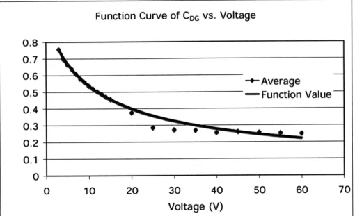
11.1.6 - 9 for the graphs of the functions and calculated parameters for CDG and CDS. Coss vs. Voltage 2.5 2132 4-B3 1.5 84 -"-85 1 0.5 0 0 20 40 60 80 Voltage (V) Cc vs. Voltage 7 6 -8B2 3 -- 83 " B4 2 -85 1 1 0 20 40 60 80 Voltage (V)
Coss, Ciss, and Cc versus Drain-Source voltage graphs for B2, B3, B4, and B5
Figure 11.1.5 These charts illustrate the capacitances measured for each of the devices B2, B3, B4, and B5.
The model for capacitance vs. voltage used to match the data is:
C
0
V
*D
(2.1.6)Parameters were selected to match each of the Average and Maximum curves of CDG and CDs versus voltage. In each case, three data points (VI, C1, V2, C2, V3, C3) from
a curve were chosen from which a fit was determined. The data points were selected to yield a good overall match to the curves. It was found that selecting data points at V=3, 9, and 15 V yielded a good overall match to the curves.
Ciss vs. Voltage 5.3 5.2 5.1 - 82 5 -B3 B84 4.9 -- BS 4.8 4.7 f 4.6 = 4.5 0 20 40 60 80 Voltage (V)
The value of parameter b was calculated by finding the zero of the function:
In(o + V2)-ln(ob+ V,) In(C/C 2) (2.1.7)
f(#)-
(2.1.7)In( + V3)-ln(o + V,) In(C, /C3)
This value of 0 was calculated numerically in MATLAB as the zero of the function
given input values for Vi, CI, V2, C2, V3, C3
-Values for m and Co were then calculated as:
ln(C,/C2) ln(CIC3)
m = Or m = (2.1.8)
In( + V2)-ln(o + V) In( + V3)- In( + V()
And
Co (1+ ) or Co 2 m Or Cjo = C3(1+ m (2.1.9)
After identifying candidate values of 4, m, and Cjo, using this method for given points (e.g., capacitances at V=3, 9, and 15 V) the function was plotted on top of the raw data graphs to verify a good fit to the data.
The Parameters of the function that best fit our average data for CDG were:
=
7.12 V= 3m =0.6441 When
=
9Cjo = 0.9500 IV = 15
Figure 11.1.6 Average CDG plot comparison for function fitting and measurement
The Parameters of the functions that best fit our average data for CDS were:
=5.67
IV,=3
m= 0.9774
I2
=9
Co = 2.143 When V = 151
Giving the function graph:
Function Curve of CDS VS. Voltage
1.6 1.4 1.2 1 - Average 1 -Function Value 0.8 0.6 0.4 0.2 0 10 20 30 40 50 60 70 Voltage (V)
The Parameters of the function that best fit our maximum data for CDG were: 0=6.67 m = 0.6760 C = 1.131 17 _
I
V= 3 WhenV3 =151
=2 1
Giving the function graph:
Function Curve of CDG vs. Voltage
1-0.9 0.8 0.7 -- Maximum S-- Function Value 0.6 0.5 0.4 0.2 0.1 0 0 20 40 60 80 Voltage (V)
Figure II1.1.8 Maximum CDG plot comparison for function fitting and measurement
The Parameters of the functions that best fit our maximum data for CD were:
= 6.04
V=
3m = 0.9786 V2
=9
Cj0 = 2.136 When 3 15
Giving the function graph:
Function Curve of Cos vs. Voltage 1.6 1.4 1.2 1 +Maximum - Function Value 0.8 0.6 0.4 0.2 0 10 20 30 40 50 60 70 Voltage (V)
11.2 On-resistance Measurement
Conduction loss of a device is linear proportional to its on-resistance. In high power area, conduction loss is a one of the dominant loss mechanisms in the converter. As a result, the FITMOS on-resistance is also important to us. This section describes the measurement of the Toyota FITMOS device On-Resistance versus Temperature.
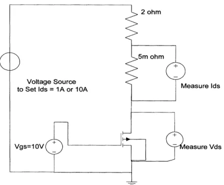
11.2.1 Measurement Methods
The circuit for making measurements is shown in Fig.II.2.1. In order to turn on the FITMOS device, a 10V Gate-Source bias voltage was applied with a DC power supply (Tektronix PS280). In addition, a current-limited DC power supply (HP
6011A) in series with a 2 Q power resistor was used to apply either 1A or 10A
Drain-Source current to the MOSFET. A multimeter (Agilent 34401A) was used to measure the drain-to-source voltage across the MOSFET. To make an accurate measurement of the Drain-Source current (IDs), a 5m f2 current-sense resistor was placed in series with the 2 Q resistor and the Drain-Source port of the MOSFET. A multimeter (Agilent 34401A) was used to measure the voltage across the 5m 0 resistor. In this way, we were able to calculate the On-Resistance by using the Ohm's Law, Ron = VdsIds. Since we want a plot for On-Resistance versus temperature, the MOSFET was clamped to a hot plate (Omega LHS-720) via an electrically insulating pad. The hot plate was used to control the case temperature of the MOSFET.
On-resistance measured from 25 'C to 150 oC was taken in 25 oC increments (i.e. 25, 50, 75...).
to . I A o. I A Measure Ids
to Set Ids= 1A or 10A
Vgs=1OV -~ easure Vds
Figure II.2.1 Circuit setup for the FITMOS On-Resistance measurements.
A 10V Vg, was applied. A DC current source was used to apply either 1A or 10A Drain-Source current for the measurement.
11.2.2 Measurement Result
From the measurement, we can see that the on-resistance measurement is consistent with different Drain-Source current level. The Rds-on is about 5.250 at the room temperature T = 25 'C and it goes up to 8.2592 when the temperature is
Aver age on- r esi st ance vs Term 8.5 8.25 _ 7. 75 7.5 %7. 25 7-• 6.75 ; 6.5 • 6. 25 ,, 6a 5. 75 5.5 __ 5.25 5 4.75 4.5 0 25 50 75 100 125 150 175 Terp (Q
axi rrum on- r esi st ance vs Tern
8.5-8. 25 7.75 7.5 ~7. 25 -) 7-~6.75
S6.5
_ S6. 256-6 5.75 - _ 5.5 5. 25 5-4.75 4.5 0 25 50 75 100 125 150 175 Ternp (Q
Figure 11.2.2 The average and maximum FITMOS On-Resistance versus temperature when the Drain-Source (Id,) current is equal to 1A.
rxi
mum on- r esi st ance vs Termp
8.75 8.5 8. 25 8 7. 75 S7. 5 )7. 25
7-26.75
6.5 16.25 _, r 55.75 __ - A _ 5.5 _ 5. 25 5 4.75 4.5 0 25 50 75 100 125 150 175 Terrp (QFigure 11.2.3 The average and maximum FITMOS On-Resistance versus temperature when the Drain-Source (Ids) current is equal to 10A.
Aver a.e on- r esi st ance vs Tenp
8.5 8.25 8 7.75 7.5 7.25 Gao 7 B 6.75 " 6.5 S6.25 S 6 S5. 75 5.5 5. 25 5 4.75 4.5 0 25 50 75 100 125 150 175 Tenp (Q
11.3 Threshold Voltage Measurement
Threshold voltage is an important parameter for a device. It determines the minimum gate voltage for the converter. Furthermore, threshold voltage is also critical for our later IV characteristic modeling. We define the threshold voltage as the required gate-source voltage Vg, to give ImA drain-source current Id.
.3.1 Threshold Voltage Measurement Methods
The circuit for making measurements is shown in Fig.II.3.1. A DC power
supply (Tektronix PS280) was used to sweep the Gate-Source voltage of the MOSFET. Between the power supply and the gate of the MOSFET, a 50K C resistor was added to prevent the DC power supply from oscillating. In addition, a current-limited DC power supply (HP 6011A) in series with a 2 9 power resistor was used to apply either
5V or 10V supply voltage. A multimeter (Agilent 34401A) was used to measure the
gate-to-source voltage across the MOSFET. For the drain current measurement, a multimeter (Agilent 34401 A) was used to measure the voltage across the 2 ! resistor. In this way, we were able to calculate the drain current by using the Ohm's Law, Is = Vd/R. The MOSFET was clamped to a hot plate (Omega LHS-720) via an electrically insulating pad. So the off hot plate acted like a huge heat sink for the MOSFET.
Measure Ids
vgs=1uv - easure Vds
Figure II.3.1 Circuit setup for the FITMOS Threshold voltage measurements.
A 5V or 10V VDD was applied. A DC voltage source was used to sweep the Gate-Source voltage for this measurement. The Drain-Source current is measured from the volt-meter across the 2 0 resistor.
11.3.2 Data and Summary
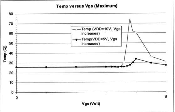
The threshold voltage was defined as the gate-source voltage when the drain-source current is ImA. An average of 3.16V threshold voltage was measured for our samples.
On average, the FITMOS has a 3.16V threshold voltage. On the temperature versus gate-source voltage graph, when the Vgs is less than threshold voltage, the device is off, so the device temperature is low. Once the Vgs is slightly above the threshold voltage, the device is on. But the device has large Vds and the device is in saturation region. At this region, the device experiences large current and large voltage drop, so there is big power dissipate on the device and hence the device temperature increases. If the gate-source voltage keeps increasing, the device will go
dissipate on the device is low, so the temperature drops back.
Ids versus Vgs (Maximum)
5000 4500 4000 - Ids (VDD=10V, Vgs increases) 3500 --- Ids(VDD=5V, Vgs 3000 increases) .2500 2000 1500 1000 500 0 0 5 Vgs (Volt)
Figure 113.2 The maximum FITMOS drain-source current versus gate-source voltage when VDD
=5V or 10V. (Current is limited by the 2 [ resistor for high Vp).
Temp versus Vgs (Maximum) 80 70 -- Temp (VDD=10V, Vgs 60 increases) -.- Temp(VDD=5V, Vgs 50 increases) o 40 S30 20 10 0 0 5 Vgs (Volt)
Figure 113.3 The maximum FITMOS temperature versus gate-source voltage when VDD =5V or
Ids versus Vgs (Average) 3500 3000 -- Ids (VDD=10V, Vgs 2500 increases) --+-- Ids(VDD=5V, Vgs increases) - 2000 _ 1500 1000 500 0 5 Vgs (Volt)
Figure II1.3.4 The average FITMOS drain-source current versus gate-source voltage when VDD
=5V or 10V
* (Current is limited by the 2 0 resistor for high Vg,).
Temp versus Vgs (Average) 60 50 40 20 20 10 ____ 0 5 Vgs (Volt)
Figure 11.3.5 The average FITMOS temperature versus gate-source voltage when VDD =5V or
10V.
- --Temp (VDD=O10V, Vgs
increases)--- Temp(VDD=5V, Vgs
11.4 I-V Characteristic Modeling
I_V characteristic is one of the most important characteristics of a device. The IV characteristic model affects the many loss mechanism in the device, ex conduction loss and switching loss. This section describes the measurement and
behavioral modeling for the Id-Vds characteristics of the Toyota FITMOS device as a
function of gate voltage. We do not seek a physical model of device behavior, but rather a simple behavioral model that can be used for rapid simulations and calculation of switching loss.
II.4.1 I-V Characteristic Measurement Methods
In the I-V curve measurement, we used the same circuit as the one we used for threshold measurement in Figure 11.3.1. The purpose of this measurement is to model the Drain-Source current in a function of Vgs (Gate-Source voltage) and Vds (Drain-Source voltage). The Gate-Source voltage of the MOSFET was set by the DC power supply (Tektronix PS280). In addition, a current-limited DC power supply (HP 6011A) in series with a 2 Q power resistor was used to apply sweep the supply voltage and hence set the Drain-Source voltage of the MOSFET. The actual Gate-to-Source voltage across the MOSFET was measured by a multimeter (Agilent 34401A). For the drain current measurement, a multimeter (Agilent 34401A) was used to measure the voltage across the 2 Q resistor. In this way, we were able to calculate the drain current by using the Ohm's Law, Ids = Vds/R. Again, the MOSFET was clamped to a hot plate (Omega LHS-720) via an electrically insulating
pad.
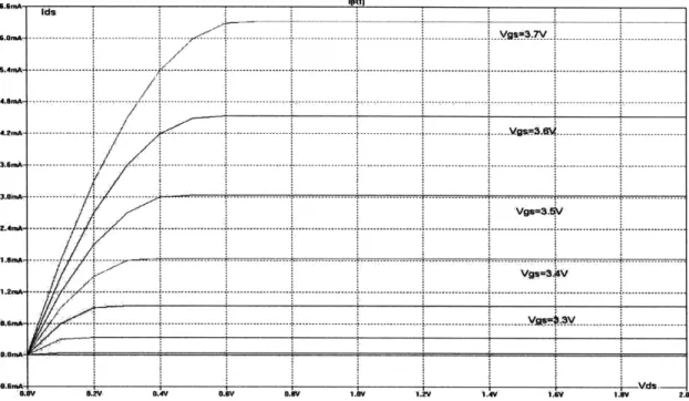
.4.2 Measurement Data
Ids versus Vds (Vt=3.16V) Measurement Average
- - Vgs=3.5V 5 -- Vgs=3.8V -- Vgs=4.OV -x- Vgs=4.1V 4 -- Vgs=4.2V -e- Vgs=4.3V 2 0 1 2 Vds (Volt)
Figure 11.4.1 Above curves show the I-V characteristic of the FITMOS.
When the V, is above 4.OV, the MOSFET heats up substantially at high simultaneous Vd. and Id current. In order to get this I-V curve with stable MOSFET temperature, the Id, was only
Ids versus Vds (Vt=3.16V) Measurement Average 10 . . -- Vgs=3.5V - Vgs=3.8V iv ... ... ... --- Vgs=4.1V -* Vgs=4.3V . -+- Vgs=4.4V - Vgs=4.5V 0.01 0 1 2 Vds (Volt)
Figure 1.4.2 The graph shows the I-V curves of the MOSFET, in which the Y-axis (I1 ) is on a
Logarithmic scale.
II.4.3 I-V Characteristic Modeling Method
In a previous section, we already described the measurement of the FITMOS I-V curves. In here, we introduce a method to model I-V characteristics of the FITMOS. The Drain-Source current is modeled as a function of Vgs (Gate-Source voltage) and Vds (Drain-Source voltage). The purpose of this model is to better capture FITMOS
I-V behavior, and hence to provide a more accurate simulation.
Figure 11.4.3 shows Id-V curves of the FITMOS parameterized by gate voltage. According to this plot, we can see that FITMOS devices exhibit operation
regions consistent with those of conventional MOSFETs, including triode operation (where current rises gradually drain-source voltage), and saturation operation (where current rises more slowly with drain-source voltage). For simplicity, we seek to model behaviors in these two regions as follows: in triode region we model the drain-source
current as linearly proportional to drain-source voltage, with a slope that is 1/Ron resistance; in the saturation region we model the drain source current as a function of K(Vgs-Vt)^a+Vds. So in order to model this I_V curve well, we need to figure out the following relations: 1. the 1/Ron as a function of Vgs; 2. the parameters K, Vt and a for K(Vgs-Vt)^a in saturation region, and 3.the slope L as a function of (Vgs-Vt).
Ids versus Vds ( Vt=3.16V) Measurement Average
6 - Vgs=3.5V 5 -.- Vgs=3.8V - Vgs=4.0V 4 Vgs=4.1V -- Vgs=4.2V -4- Vgs=4.3V 3 -- Vgs=4.4V -Vgs=4.5V 2 0 Vds (Volt)
Figure 11.4.3 The average I-V curve of the FITMOS. The average threshold voltage is 3.16V.
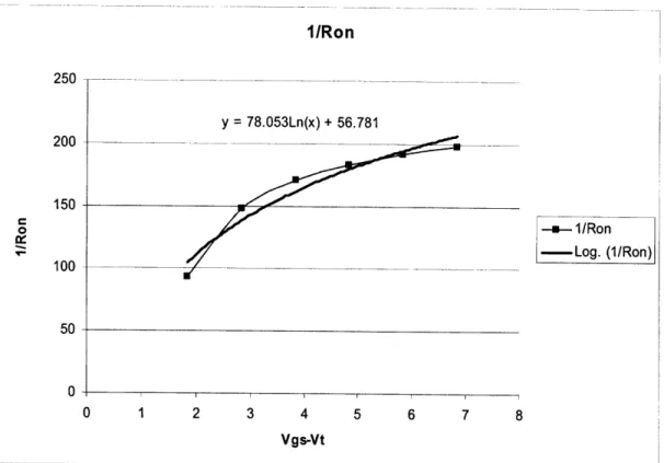
11.4.3.1 1/Ron Function
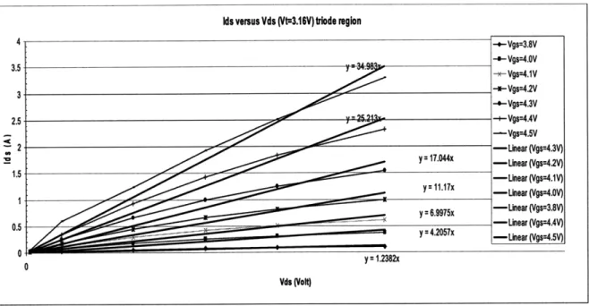
From the I-V curve in Figure 11.4.3, we can see that the current Ids is linearly proportional to 1/Ron when Vds is small. Figure II.4.4 focuses on the triode region of the I-V curve extracted from figure 11.4.3. For simplicity and based on empirical observation, we treat the FITMOS device as being in triode region when Vd is less than 0.2 V.
Ids versus Vds (Vt=3.16V) triode region 4 -- Vgs=3.8V S- Vgs=4.0V 3.5 y ne4. -- Vgs-4.1V 3 -- Vgs=4.2V -e-Vgs=4.3V 2.5 - -+-Vgs=4.4V y 17.044x -Linear (Vgs=4.2V) y=17 -Linear (Vgs=4.1V) -Linear (Vgs:3.8V) 0.5 y 4.2057x - Linear(Vgs=4.4V) Linear (Vgs-4.V) 0 y =1.2382x Vds (Volt)
Figure HI.4.4 The Triode regions of the FITMOS, linear trendlines are added to model the 1/Ro. From the trendline equations, we can see that 1/1R. is the slope of each line according to I=V/R.
As a result, from the slope of each line in figure 11.4.4, we can find out the 1/Rn value for each Vs. Figure 11.4.5 shows a curve fit the 1/Ron in a function of Vg,-Vt in triode region for low value of Vgs-Vt, which is:
= 9.3495*(V, -V) 4
*543 1 (2.4.1)
Ron
I /Ron for triode region Only
40 35- Y AO4.5431 R2 = 0.9999 30 25 ---- 1/Ron 20 - Power (1/Ron) 15 10 5 0 0.5 1 1.5 Vgs-Vt
Figure II.4.5 This plot shows the 1/R,. versus V,-V,.
While this curve matches for voltage slightly above threshold, we know that the l/Ron will not keep on increasing to infinity as Vgs-Vt continues to increase. To account for this, we measured the Ro, versus Vgs for larger value of Vgs as well. The measurement setup is the same as the setup we used in a previous section on On-resistance versus temperature. The setup is shown in Figure 11.4.6.
2 ohm
Voltage Source
to Set Ids = 1A Measure Ids
Vgs +easure Vds
Figure 11.4.6 Measurement setup for R,, versus Vg,.
We set the Ids to 1A and measure the Vds across the FITMOS, then we can calculate the On-resistance from R=V/I. Ron was measured from Vgs = 5V to 10 V with lv increments.
Figure 11.4.7 shows the 1/Ron versus Vgs-Vt for both triode small and large
values of Vgs. We can see that 1/Ron reaches its maximum when Vgs is large. When
Vgs is equal to 10V, 1/Ron is about 200 Q-1 and hence Ron is about 5mg. This is
consistent with our previous On-resistance versus temperature measurement results, in which we have the On-resistance as about 5mQ at room temperature.
Figure II1.4.7 1/Ron versus (Vgs-Vt) for both triode and saturation region (Vt=3.16V).
As a result, we cannot model the 1/Ron in a power function of Vgs when Vgs is
high, otherwise, it will grow to a very large number which is not consistent with our 5m C1 on-resistance limit. So we model the 1/Ron in a different function when Vgs is large. Figure 1I.4.8 shows the 1/Ron curve for large Vgs. In this region, a logarithmic function can fit the curve very well:
S= 78.053Ln(Vgs - V,)+56.781 (2.4.2)
1I/Ron 250 200 150 y = 78.053Ln(x) + 56.781 100 50
0
0 1 2 3 4 5 6 7 8 Vgs-VtFigure II.4.8 1/Rn versus Vgs,-Vt curve when Vg, is large
The Log function trendline shows the function to model the 1/Ro. for large Vg,.
In conclusion, we model the l/Ron as a conditional function:
R = If ((V - V) < 1.6734, 9.3495 * (V, - V)45 431
,78.053Ln(Vg, - V,) + 56.781)
R01
(2.4.3)
Where 1.6734 is the intercept between these two functions, when the If statement is true, function 9.3495 * (Vgs, - V)45431 is used, otherwise, 78.053Ln(Vg, - V) + 56.781 is used.
For small Vgs, when the 1/Ron increases rapidly with Vgs, we model it with a power function 9.3495 * (Vgs - )4.5431. When Vgs is large, we use the Logarithmic
function 78.053Ln(Vg -V,)+56.781 to model 1/Ron to control it within the
reasonable physical limit, which is about 200 to 300 -1' since on-resistance is about
with the measured value. We can see that our model fits the measurement result very well.
1IRon Model Comparison
250 200 150 0-- 1/Ron measurement - -- 1/Ron model 100 50 0 0 1 2 3 4 5 6 7 8 Vgs-Vt
Figure 11.4.9 The comparison between our model for 1/Ron and the measurement result. Our model fits quite well with the measurement.
11.4.3.2 K( -Vrt)^a in saturation region
At high levels of drain-source voltage (e.g., above 0.2V), the FITMOS seems to get into the saturation region and the slope of the I-V curve is reduced. In this case, we try to model the drain-source current with a function K(Vgs-Vt)Aa + XVds. X is the slope of the I-V curve in saturation region. K(Vgs-Vt)Aa is the intercept of the extended I-V trendline in saturation and the y-axis, which is Vds=O. In order to obtain the as K(Vgs-Vt)^a function in saturation, the I-V curve in saturation was extracted. Figure 11.4.10 shows the I-V curve in saturation region.
Ids versus Vds (Vt=3.16V) Saturation region
Figure 11.4.10 The I-V curve in saturation region only.
From the trendline equations for the drain-source current Ids, when x (Vds) = 0, we have values for K(Vgs-Vt)a. Figure 11.4.11 shows the K(Vgs-Vt)0a versus (Vgs-Vt) plot. If we model the K(Vgs-Vt)^a curve as a power function, we have:
K = 0.9172 a =4.3406 (2.4.4) K(Vg- Vt)^ = 0.9172* (Vgs- Vt) 4.3406 K(Vgs-Vt)^a 3.5 y = 0.9172X 4 .340 6 3 R2 2.5 -- K(Vgs-Vt)^a 1.5 ---- Power (K(Vgs-Vt)Aa) 0.5 0-0 0.5 1 1.5 Vgs-Vt
Figure 11.4.11 K(Vgs-Vt)A versus (Vgs-Vt) plot
11.4.3.3 slope A modeling
From the trendline equation in figure 11.4.10, we also can obtain the value for the slope of the I-V curve X in the saturation region. In figure 11.4.12, the slope X versus (Vgs-Vt) is plotted. Again, from the power trendline, we can get the slope X in a
function of (Vgs-Vt): A = 0.6122* (Vg, -V,)71 6 (2.4.5) Theoretical A 10 9 8 7 6 S5 4 3 2 1 y = 0.6122xL" 8 R2= 0.9868 -Power (A) 0 0.2 0.4 0.6 0.8 1 1.2 1.4 1.6 Vgs-Vt
Figure 11.4.12 The slope of the I-V curve k in saturation region versus Vg,-Vt. From the power trendline, a can be expressed as a function a Vg,-V,.
As a result, in the saturation region, we can express the drain-source current Ids in a function of Vgs-Vt and Vds:
Ids = K(Vg - V,) + *Vd (2.4.6)
= 0.917 2 * (Vgs- V
,)4.3406 + 0.6122 * (Vg, -V)87186 * Vd
II.4.4 FITMOS I- V Model equations and data
From our above analysis, we can express the FITMOS I-V curve as different
-equations in triode region and saturation region.
In triode region (modeled as the range Vd, < 0.2V), the drain source current is modeled as linearly proportional to drain-source voltage, with a slope 1/Ron that is a function of Vgs:
V
I, = = If ((Vgs - V,) < 1.6734, 9.3495 *(V - t )4.54 31,78.053Ln(Vgs - V) + 56.781)* Vd
Ron
(2.4.7) When the Vds > 0.2 V, the FITMOS gets into saturation region:
d, = K(Vgs -Vt)" + 2 * Vds
(2.4.8)
=0.9172 *(V, - Vt)43406 + 0.6122 *(Vg, -V)8.7186 * Vs
In the end, we combine these two equations into a conditional function:
I, = MIN(If ((Vgs - V,) 1.6734, 9.3495 * (Vg - V,)4.5431,78.053Ln(Vgs - V,) + 56.781)* V,
0.9172* (Vgs- Vt )4.346 + 0.6122* (Vgs -V,)8.7186 * Vs )
(2.4.9) Figure 11.4.13 shows the I-V plot from our equation model.
For comparison, the measured I-V curve and our modeled I-V curve are plotted in figure 11.4.14; we can see that our behavioral model matches with real FITMOS I-V characteristic very well. In addition, figure 11.4.15 shows our model also works for
Ids versus Vds (Vt=3.16V) Modelling 6 -+- Vgs=3.8V 5 ~- - Vgs=4.OV - Vgs=4.1V 4 -x- Vgs=4.2V -- Vgs=4.3V Vgs=4.5V -3 2 0 0 1 2 Vds (Volt)
Figure 11.4.13 The I-V plot from our equation model.
Ids versus Vds (Average Vt=3.16V) Comparison
Mfl~p--+-Vgs=3.8V -- Vgs=4.0V - Vg s=4.1V -- Vgs=4.2V -e- Vgs=4.3V -Vgs=4.4V - Vgs=4.5V - Vgs=3.8V Model -- Vgs=4.OV Model - Vgs=4.1V Model - Vgs=4.2V Model -- Vgs=4.3V Model -. Vgs=4.4V Model -.-- Vgs=4.5V Model 0 1 2 Vds (Volt)
Figure 11.4.14 This shows the measured FITMOS I-V characteristic and our behavioral model. Our model matches with the measurement very well.
I I - -1 -1-1-II "= = ... ... -C' I ---- ~1--- ~I~PZ~T~ L L r
--/
Ids versus Vds (Vt=3.16V) Modelling 1000 .-- Vgs=3.8V -a- Vgs=4.0V 100 --- Vgs=4.1V -*- Vgs=4.2V 10 -- Vgs=4.3V -- Vgs=4.4V .:._ _ ____ __K -Vgs=4.5V 1 ~-i -- -,- Vgs=6V -- Vgs=8V 0.1 - I I r I I - - Vgs=l O.OV 0.01 0.001 0 1 2 Vds (Volt)
Figure 11.4.15 shows the modeled Id curve versus Vd, for large Vg,
For large V, (Vp > 8V), the drain source current Ids is much larger than those of relatively small
Vgs, so Id, (y-axis) is plotted on a logarithmic scale for clearer comparison.
II.4.5 Difficulties in FITMOS I-V Characteristics Modeling
In the past, the lateral MOSFET had been studied extensively. But the classical model for the current-voltage characteristics of the lateral MOSFET is based on the assumption that between drain and source only the channel resistance exists. This assumption on longer holds for the high voltage power MOS devices. Especially the FITMOS is a vertical floating island trench gate MOSFET, as a result, the conventional MOSFET model does not fit for our FITMOS devices.
In the vertical power MOSFET devices, the source and drain terminals are not only separated by the channel resistance but also all the resistances in the drain current path. Due to the special floating trench gate structure in FITMOS, the
resistances in the drain current path are not well studied. So building an analytical physical model of FITMOS requires more solid-state physics studies and device simulations. In addition, the conventional MOSFET models cannot simulate the unique power device characteristic very accurately such as quasi-saturation. As a result, building an analytical model for FITMOS is not practical in our intense
schedule.
Second, since we do not have much experience in building an analytical model for conventional power MOSFETs before, it is hard for us to compare the difficulties in FITMOS modeling and in conventional power MOSFET modeling.
On the other hand, building a behavioral model is relatively simpler and can fulfill our needs for the future design simulation.
II.4.6 FITMOS and Commercial MOSFETI-VModel Simulation Comparison
This section explores the accuracy of SPICE electrical models for conventional power MOSFETs, as provided in manufacturer's datasheets. In addition, we also compare the accuracy of our FITMOS electrical model with this manufacturer model. MOSFET FDP047AN08 is used for the test. The schematic of the test circuit is shown in Figure 11.4.16. Voltage source Vi is used to sweep the drain-source voltage Vd, of the MOSFET. Voltage source V2 is used to control the gate voltage
Vgs. A small im ohm resistor in series with the MOSFET drain is used to monitor the drain current Ids.
Im ohm
Voltage Source V1
FDPO4 N
Vgs V2
Figure 11.4.16 The schematic of the test circuit used in simulation and measurement.
First, the experimental output characteristic of the FDPO47AN is shown in figure 11.4.17. From the experimental data, the threshold voltage is measured as 2.74 V (Ids = ImA), which is in the range of the datasheet specified (2V-4V).
Figure 11.4.17 Experimental I-V characteristics of the conventional power MOSFET FDP047AN.
Figure 11.4.18 shows the threshold simulation from the manufacturer's datasheet spice model (shown in detail in the appendix). As we can see, the threshold voltage is about 3.3 V for I =mA, which is about 0.6V larger than our experimental
measurement (a wide variation of possible thresholds is allowed in the datasheet). In this case, the simulation of the I-V characteristics of this MOSFET will not match with the experimental data with the same gate voltage.
l.A ... .. ... ... ... ... w . -- ... .. .. .. ...-- ... ... ... ... .A . .
2 . i 4 .. .. . .. . ... .
O. .4 1,i ISW 2W 2. 3 3.Y iM 4.5V S.OV
Figure II.4.18 Simulation result for the threshold voltage of the FDPO47AN using the manufacturer's Pspice model.
Vt = 3.31V for Ids=lmA and Vds = 10V
Figure 11.4.19 shows the simulation of the I-V characteristics of the conventional power MOSFET using the manufacturer's Pspice behavioral model. Since the threshold voltage in the spice model is smaller than the real device, with the same gate voltage, the simulated drain current is much smaller than our experimental data.