Publisher’s version / Version de l'éditeur:
Langmuir, 19, 18, pp. 7282-7288, 2003-09-02
READ THESE TERMS AND CONDITIONS CAREFULLY BEFORE USING THIS WEBSITE. https://nrc-publications.canada.ca/eng/copyright
Vous avez des questions? Nous pouvons vous aider. Pour communiquer directement avec un auteur, consultez la première page de la revue dans laquelle son article a été publié afin de trouver ses coordonnées. Si vous n’arrivez pas à les repérer, communiquez avec nous à PublicationsArchive-ArchivesPublications@nrc-cnrc.gc.ca.
Questions? Contact the NRC Publications Archive team at
PublicationsArchive-ArchivesPublications@nrc-cnrc.gc.ca. If you wish to email the authors directly, please see the first page of the publication for their contact information.
NRC Publications Archive
Archives des publications du CNRC
This publication could be one of several versions: author’s original, accepted manuscript or the publisher’s version. / La version de cette publication peut être l’une des suivantes : la version prépublication de l’auteur, la version acceptée du manuscrit ou la version de l’éditeur.
For the publisher’s version, please access the DOI link below./ Pour consulter la version de l’éditeur, utilisez le lien DOI ci-dessous.
https://doi.org/10.1021/la034310h
Access and use of this website and the material on it are subject to the Terms and Conditions set forth at
Mesostructured MTES-derived silica thin film with spherical voids
investigated by TEM: 1. mesostructure determination
Yu, K.; Wu, X.; Brinker, C. J.; Ripmeester, J.
https://publications-cnrc.canada.ca/fra/droits
L’accès à ce site Web et l’utilisation de son contenu sont assujettis aux conditions présentées dans le site LISEZ CES CONDITIONS ATTENTIVEMENT AVANT D’UTILISER CE SITE WEB.
NRC Publications Record / Notice d'Archives des publications de CNRC:
https://nrc-publications.canada.ca/eng/view/object/?id=6f94239c-ee7d-4282-8e75-0781cd6af1a7
https://publications-cnrc.canada.ca/fra/voir/objet/?id=6f94239c-ee7d-4282-8e75-0781cd6af1a7
Mesostructured MTES-Derived Silica Thin Film with
Spherical Voids Investigated by TEM: 1. Mesostructure
Determination
K. Yu,*
,†X. Wu,
‡C. J. Brinker,
§and J. Ripmeester
†Steacie Institute for Molecular Sciences, National Research Council of Canada, Ottawa, Ontario K1A 0R6, Canada, Institute for Microstructural Sciences, National Research
Council of Canada, Ottawa, Ontario K1A 0R6, Canada, and Sandia National Laboratories, MS 1349, Albuquerque, New Mexico 87185, and Center for Micro-Engineered Materials,
University of New Mexico, Albuquerque, New Mexico 87131 Received February 21, 2003. In Final Form: May 29, 2003
The mesostructure of a hydrophobic silica thin film with spherical voids arranged in an ordered array was investigated and resolved thoroughly by transmission electron microscopy (TEM). The novel TEM approach involved sample tilting to get different zone axes and simulation, as well as the calculation of plane spacings and angles for comparison of the experimental values with the corresponding theoretical ones. The camera constant (λL) was calibrated carefully by the diffraction pattern of the silicon substrate, on which the closed-cell mesostructured thin film was developed. This film was fabricated by solvent evaporation-induced sol-gel and self-assembly processes, with methyl triethoxysilane [MTES, Si(OCH2
-CH3)3CH3] as the silica precursor and a polystyrene-block-poly(ethylene oxide) diblock as the
structure-directing agent; pyrolysis was performed carefully to remove the template. The present TEM exploration concludes that the mesostructure is exclusively body-centered cubic (bcc) rather than face-centered cubic-(fcc); this conclusion was based on the assessment of the experimental tilting angles and the theoretical angles employed to get one zone axis from another, as well as on the evaluation of the experimental and simulated TEM images. The bcc mesostructure with a slight distortion was further assigned to be body-centered tetragonal (bct) with the preferred cell parameters of a ) 13.5 nm and c ) 13.0 nm; this assignment was based on the comparison between the experimental and the calculated data, including the plane spacings and the angles between various planes. The present self-assembled MTES-derived silica thin film with closed cells arranged in a slightly distorted bcc array is believed to be the first and is a promising candidate to function as a low-dielectric-constant (k) insulating material needed for future semiconductor devices.
1. Introduction
A great deal of interest in the synthesis of various mesostructured porous inorganic oxides emerged in 1992;1
since then, a large variety of surfactant-templated silica materials have been synthesized in the form of powders, particles, and thin films.2-4Mesoporous materials in the
form of thin films are good candidates for various applications such as hosting optically active or quantum confined species as sensors. Furthermore, it has been proposed that the introduction of pores into silica, which ideally should be nanosized voids (isolated rather than interconnected) with a uniform distribution will lead to the next generation of dielectric insulators with low dielectric constants (k).5Preferential solvent
evaporation-induced sol-gel and self-assembly (EISGSA) processes
at ambient temperature and pressure have brought a new perspective to the fabrication of silica/surfactant hybrid thin films with well-ordered mesostructures.4However,
after pyrolysis, the mesostructured pores are usually interconnected through micropores in the silica wall; in addition, the hydrophobicity of tetraethoxysilane-derived silica thin films is low.
We first reported on the use of PS-based amphiphilic diblock copolymers with a high glass transition temper-ature (Tg ≈ 373 K), namely,
polystyrene-block-poly-(ethylene oxide) (PS-b-PEO) diblocks, to synthesize silica/ amphiphile thin films with regular and reverse meso-phases, as well as curved multilamellar mesostructures, through the so-called EISGSA processes.6 Among the
usually observed mesophases there was a brand-new one consisting of an ordered arrangement of spherical mi-crodomains that were isolated from each other.
In the fabrication of this mesophase, tetraethoxysilane [TEOS, Si(OCH2CH3)4] and methyl triethoxysilane [MTES,
Si(OCH2CH3)3CH3], as well as a mixture of MTES and
TEOS, were used as silica precursors.7 The synthetic
approach was designed to suppress the silicate condensa-tion, to allow co-self-assembly (of the silicates and the
* To whom correspondence should be addressed.
†Steacie Institute for Molecular Sciences, National Research Council of Canada.
‡Institute for Microstructural Sciences, National Research Council of Canada.
§Sandia National Laboratories and University of New Mexico. (1) Kresge, C.; Leonowicz, M.; Roth, W.; Vartuli, C.; Beck, J. Nature 1992, 359, 710.
(2) (a) Huo, Q.; Margolese, D. I.; Clesla, U.; Feng, P.; Gler, T. E.; Sleger, P.; Leon, R.; Petroff, P. M.; Schuth, F.; Stucky, G. D. Nature 1994, 368, 317. (b) Tanev, P. T.; Pinnavaia, T. J. Science 1995, 267, 865. (c) Smarsly, B.; Goltner, C.; Antonietti, M.; Ruland, W.; Hoinkis, E. J.
Phys. Chem. B 2001, 105, 831.
(3) (a) Antonelli, D. M.; Ying, J. Y. Angew. Chem., Int. Ed. Engl. 1995, 34, 2014. (b) Mann, S.; Ozin, G. A. Nature 1996, 382, 313. (c) Ozin, G. A.; Chomski, E.; Khushalani, D.; Maclachlan, M. J. Curr. Opin. Colloid
Interface Sci. 1998, 3, 181.
(4) (a) Ogawa, M. J. Am. Chem. Soc. 1994, 116, 7941. (b) Brinker, C. J.; Lu, Y.; Sellinger, A.; Fan, H. Adv. Mater. 1999, 11, 579.
(5) Miller, R. D. Science 1999, 286, 421.
(6) Yu, K.; Hurd, A. J.; Eisenberg, A. Brinker, C. J. Langmuir 2001,
17, 7961.
(7) (a) Yu, K.; Smarsly, B.; Brinker, C. J. Mater. Res. Soc. Symp.
Proc. 2002, 728, S1.9. (b) Yu, K.; Smarsly, B.; Brinker, C. J. Adv. Funct. Mater. 2003, 13 (1), 47-52. (c) Smarsly, B.; Xomeritakis, G.; Yu, K.;
Liu, N.; Fan, H.; Assink, R. A.; Drewien, C. A.; Ruland, W.; Brinker, C. J. Langmuir 2003, 19, 7295-7301. (d) Smarsly, B.; Yu, K.; Brinker, C. J. Stud. Surf. Sci. Catal. 2003, 146, 295-298.
10.1021/la034310h CCC: $25.00 © 2003 American Chemical Society Published on Web 08/06/2003
template) accompanied and followed by the careful PEO retraction from the sol-gel matrix, leaving no additional microporosity, without gas permeability due to the continuous rearrangement of the matrix and consolidation. Mesostructured silica thin films with closed cells as well as with tuneable hydrophobicity were obtained after careful pyrolysis.7Various experiments, such as thermal
gravimetric analysis, surface acoustic wave nitrogen adsorption, contact-angle measurements, 13C and 29Si
direct polarization magic angle spinning solid state nuclear magnetic resonance spectroscopies, and two-dimensional grazing incidence small angle X-ray scattering (GISAXS), were carried out to characterize the as-prepared and calcined thin films in detail. A solvent-mediated mech-anism was proposed to account for the absence of mi-croporosity, namely, the absence of the interconnectivity of the mesopores. The quantitative absence of additional microporosity in the matrix (after PEO removal) was demonstrated by GISAXS with a theoretical approach, the so-called chord-length distribution. For the meso-structure, the GISAXS experiment favored a body-centered cubic (bcc) lattice, without giving conclusive results between bcc and face-centered cubic (fcc) lattices because of a lack of three-dimensional information about the pore arrangement. A bcc mesostructure throughout the whole film (and not only locally), with a slight distortion and a lattice parameter of about 13.0 nm, was recom-mended.7 Nevertheless, the transmission electron
mi-croscopy (TEM) study left the structural distinction of bcc versus fcc unresolved.7
With respect to the self-assembly of the diblock in the fabrication process, it is also difficult to determine unambiguously whether the ordered structure is bcc or fcc in nature. It is necessary to point out that self-assembly in the present system goes through different concentration regions.8Therefore, a brief description of the self-assembly
of diblock copolymers in dilute, semidilute, and concen-trated solutions, as well as in the bulk, is provided. Although this introduction is qualitative and highly simplified, it is of help to have an overview of the compulsory requirements for the investigation of bcc vs fcc structures in the present system. In general, spherical micelles form in a dilute solution of a selected solvent at a fixed temperature when micellization occurs.9In
semi-dilute and concentrated solutions, there is a general agreement that gelation takes place because of the population increase of spherical micelles with increasing temperature; both fcc and bcc structures have been observed, but not the simple cubic (sc) ones.10The volume
fractions (Φ) of spheres in various cubic systems are different and can reach values as high as 0.74, 0.68, or 0.49 in a fcc, bcc, or sc structure, respectively.11In the
bulk, the morphologies (including bcc-organized spheres, hexagonal-arranged rods, and lamellae) of microphase-separated AB diblock copolymers are usually a function of the copolymer composition, namely, the volume ratio of the two blocks.12It is acknowledged that the formation
mechanism of the mesostructured silica/PS-b-PEO thin
films is of interest;8however, the present study does not
address this feature, but only the mesostructural dilemma of bcc versus fcc.
In the present publication, we report on the determi-nation of the mesostructure of the MTES-derived silica thin films with ordered voids using TEM. By this approach, the mesostructure is determined unambiguously to be slightly distorted bcc and is cautiously assigned to be a body-centered tetragonal (bct) structure with the cell parameters of a ) 13.5 nm and c ) 13.0 nm. The present self-assembled MTES-derived silica thin film with isolated bct-arranged voids provides a conceptual route to the fabrication of materials with nanosized voids arranged in a cubic array as well as with controllable hydrophobicity, whose k values could be extended promisingly to the ultralow k range (k < 2.2).5
2. Experimental Section
Mesostructured silica films were prepared by EISGSA; a detailed description can be found elsewhere.6-8The synthesis
began with a tetrahydrofuran solution containing PS(35)-b-PEO-(109) diblock copolymer (with 35 styrene units and 109 ethylene oxide units from Polymer Source, Inc.), MTES, and hydrogen chloride (HCl), as well as Milli-Q water; a weight ratio of about 1:7 copolymer/MTES as well as molar ratios of 1:0.004:5 MTES/ HCl/H2O were acquired. After one drop of the solution was cast
onto the surface of a (001) silicon (Si) wafer (ca. 0.54 mm in thickness) and subsequent gelation, pyrolysis was carried out in argon (with a heating rate of 1 °C/min to 400 °C for 3 h) to remove the template and to produce a non-free-standing silica thin film with nanosized spherical voids arranged in an ordered array. The mesostructure of the calcined MTES-derived silica thin film on the Si wafer was characterized by TEM. Two methods of TEM sample preparation were carried out: one was by scratching; the other was by using the cross section. The first sample was prepared by scratching the film with a pair of tweezers and directly dispersing fragments onto a holey TEM carbon-coated copper grid. For the cross-sectional sample, two bars (ca. 1 mm in width and 4 mm in length) were cut out of the wafer and glued together with the film sides face to face; the glue used was M-bond 610 transparent epoxy (Measurements Group, Inc., Raleigh, NC). Afterward, a disk (3 mm in diameter in the central part) was constructed from the glued object with an ultrasonic disk cutter (Gatan, model 601). This disk was thinned mechani-cally from about 1 mm to about 100 µm in thickness. The thinned disk was dimpled from both sides with 3 µm of diamond paste, until its central part reached approximately 20 µm in thickness. The dimpled disk was then polished from both sides with 1 µm of diamond paste to achieve very smooth surfaces. A final thinning to perforation was conducted using Ar ion milling (Precision Ion Polishing System, Gatan, model 691) from both sides with an ion beam angle of 8° and a gun voltage of 6 kV. The TEM samples were loaded in a double tilt sample holder and examined in a Philips EM 430T operated at 200 kV. The relativistic wavelength (λ) of the electron at a 200-kV accelerating voltage is 0.0251 Å.
3. Results and Discussion
As was mentioned before, the present self-assembled sol-gel MTES-derived silica thin film with spherical voids on a nanometer scale and organized in an ordered array is a promising candidate for low-k dielectric materials in future micro-electronic devices. In the preparation of such silica/PS-b-PEO hybrid thin films as well as subsequent pyrolysis, a number of factors and the interplay between them influence both the meso- and microstructures.6-8In
general, our synthetic design was aimed at the formation of spherical microdomains with the co-self-assembly to be accompanied by a PEO retraction from the matrix but without leaving additional microporosity. Also, the design
(8) Yu, K.; Drewien, C. A.; Hurd, A. J.; Brinker, C. J.; Eisenberg, A.
Mater. Res. Soc. Symp. Proc. 2001, 672, O8.15.
(9) (a) Price, C. In Developments in block copolymers; Goodman, I., Ed.; Applied Science Publishers: London, 1982; Vol. 1, p 39. (b) Halperin, A.; Tirrel, M.; Lodge, T. P. Adv. Polym. Sci. 1992, 100, 31. (c) Gao, Z.; Varshney, S. K.; Wong, S.; Eisenberg, A. Macromolecules 1994, 27, 7923. (d) Yu, K.; Bartels, C.; Eisenberg, A. Langmuir 1999, 15, 7157. (10) (a) McConnell, G. A.; Gast, A. P.; Huang, J. S.; Smith, S. D. Phys.
Rev. Lett. 1993, 71, 2102. (b) Wanka, G.; Hoffmann, H.; Ulbricht, W. Macromolecules 1994, 27, 4145.
(11) (a) Hoover, W. G.; Ree, F. H. J. Chem. Phys. 1968, 49, 3609. (b) Scordari, F. Ionic Crystals. In Fundamentals of Crystallography;
Giacovazzo, C., Ed.; Oxford University Press: Oxford, 1992; p 429. (b) Bates, F. S.; Fredrickson, G. H. Annu. Rev. Chem. 1990, 41, 525.(12) (a) Matsen, M. W.; Bates, F. S.; Macromolecules 1996, 29, 1091.
was endeavored to allow the template decomposition products to diffuse out through the matrix at the early stages of pyrolysis; however, the matrix became gas impermeable at the later stages of this process. Although the GISAXS experiment confirmed the quantitative absence of additional microporosity, these studies did not reach a final conclusion as to whether the ordered array of the nanosize voids is bcc or fcc in nature.6-8To determine
unequivocally the three-dimensional mesostructure as well as the unit-cell parameters, a novel TEM approach was developed. It involves systematic simulation of sample tilting and a comparison of the experimental data with theoretical values of the plane spacings and angles. In consequence, the Results and Discussion section consists of three parts. The study of tilting for the achievement of different zone axes of the mesostructurd thin film is presented in the first part. The simulation of TEM images is addressed in the second part. The third part contains the comparison of the experimental data with theoretical values of the plane spacings and angles.
3.1. Tilting Experiments To Acquire Several Zone Axes. The cross-sectional TEM sample was studied first.
Figure 1a is a representative TEM image of both the film and the substrate; this image was recorded after the sample was tilted slightly to get the Si[110] zone axis. Figure 1b presents the diffraction patterns acquired from the circled area in Figure 1a, with the camera length L ) 2900 mm; the diffraction patterns of the film and the substrate were recorded simultaneously. The Si diffraction spots in Figure 1b are indexed with the subscript Si. The central part of Figure 1b is shown in Figure 1c with an enlargement factor of 10, the diffraction pattern of which is from the film. Parts b and c of Figure 1 demonstrate that the Si[001] direction [the so-called z axis that is perpendicular to the surface (001) of the wafer on which the sol-gel thin film was developed] is also a certain direction (identified as t1and indicated in Figure 1c) of
the film. This is due to the fact that both 002 and 0,0,-2 Si diffraction spots and two film diffraction spots are lined up along this z axis.
From now on, only the silica thin film is addressed; all the diffraction patterns were recorded with L ) 2900 mm and the ones presented have an enlargement factor of 10. With this t1direction as the tilting axis, the sample was
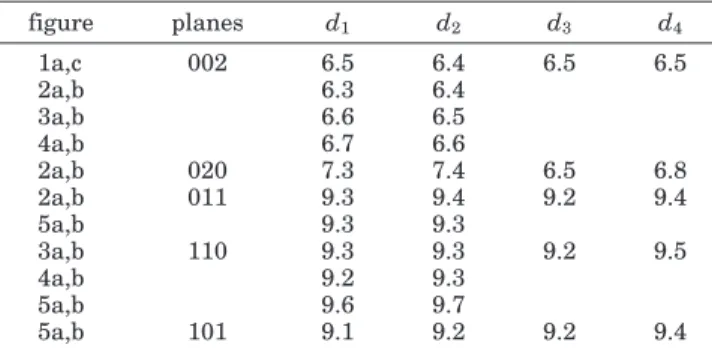
tilted 16° from the Figure 1 position, and a low-index zone axis was obtained. The TEM image is presented in Figure 2a, and the corresponding film diffraction pattern is shown in Figure 2b. For the film TEM image (Figure 2a), the regions with increased brightness compared to that of their surroundings are organized in a parallelogram-like array; they are hollow spheres rather than cylinders by nature. The sizes of these bright spots are very uniform. Moreover, from the Figure 1 position, also along this t1
direction, the sample was tilted 29° in the opposite direction (comparing Figure 1 to Figure 2), and another low-index zone axis was obtained; the TEM image and the corresponding film diffraction pattern are presented in parts a and b of Figure 3, respectively.
It is helpful to point out that the zone axes of the film shown in Figures 1-3 should be of the [u,v,0] type, because [001]‚[uvw] ) 0 gives w ) 0. Hence, a sc structure can be
Figure 1. (a) Representative TEM image of the cross-sectional sample prepared, showing both the silica film with spherical voids arranged in a cubic array and the Si substrate. (b) Diffraction patterns of both the film and the substrate recorded at the same time with L ) 2900 mm. The indices for Si are presented with the subscript Si; the Si zone axis is [110]. (c) Enlarged diffraction pattern of the film by a factor of 10, the indices are for the mesostructure being bcc [720].
Figure 2. Cross-sectional sample tilted 16° from that in Figure 1a with t1 as the tilting axis: (a) the TEM image, (b) the
diffraction pattern, and (c) indices for bcc [100].
Figure 3. Cross-sectional sample tilted 29° from that in Figure 1a in an opposite direction (compared to the one from Figure 1a to Figure 2a), still with t1as the tilting axis: (a) the TEM
easily ruled out because of the fact that for a sc arrange-ment the TEM images as well as their corresponding diffraction patterns of the [u,v,0] zone axes are always square or rectangular and are not the same as the ones shown in parts a and b of Figure 2, respectively.
Following the cross-sectioned sample, the scratched sample was studied, and two zone axes were obtained. This sample was tilted first to get the same zone axis as that shown in Figure 3; one TEM image and its corre-sponding diffraction pattern are demonstrated in parts a and b of Figure 4, respectively. From the position in Figure 4, with the t2direction (indicated in Figure 4b) as a tilting
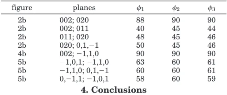
axis, the sample was tilted 34° to get a fourth low-index zone axis; the TEM image as well as its corresponding diffraction pattern are shown in parts a and b of Figure 5, respectively.
Subsequently, four zone axes (Figures 1-5) are obtained from the tilting experiments. According to the feature of each TEM image and its corresponding diffraction pattern
presented in Figures 2-5, however, the possible zone axes of Figures 2, 3, and 5 can either be bcc [100], [110], and [111], respectively, or fcc [110], [100], and [111], respec-tively. Consequently, it is still a thorny issue to differenti-ate the arrangement of the spherical voids in the film to be bcc or fcc based on our experimental TEM tilting results. Accordingly, the experimental tilting angles are used to fit the theoretical angles required, when one zone axis is tilted relative to another, under the assumption that the mesostructure is bcc or fcc. Table 1 presents the experimental tilting angles from Figure 1 to 2 and 3, as well as from Figure 4 to 5. In addition, the corresponding zone axes fitted, as well as the theoretical angles between the two fitted zone axes, are summarized in Table 1 in columns 3 and 4, under the assumption of bcc and fcc mesostructures, respectively.
Table 1 illustrates that the zone axis of Figure 1c is bcc [720] or fcc [950], fitting with the tilting angles needed to get Figures 2 and 3. In addition, Table 1 demonstrates that the zone axis of Figure 5 is bcc [111] or fcc [302], to match up the experimental tilting angle of 34° used from Figure 4 to 5. As a result, it seems highly reasonable to recommend the mesostructure to be bcc rather than fcc as a result of the fact that the characteristics of the TEM image and diffraction pattern shown in Figure 5a,b are comparable with those of bcc [111] and not fcc [302].
In conclusion, one (001) standard stereographic projec-tion of the cubic structures (both bcc and fcc) is demon-strated in Figure 6. The corresponding zone axes shown in Figures 1-5 are designated as points and labeled in Figure 6 to have a clear view of the relationship between the various zone axes of a bcc or fcc arrangement regarding the tilting experiment. The starting position (Figure 1c) can be either bcc [720] or fcc [950], and the [100] and [110] zone axes can be achieved when the tilting is performed along the [001] direction (namely, in the x-y plane perpendicular to the z axis), with 16° in one direction and 29° in another direction. However, from the zone axis bcc [110] or fcc [100], the zone axis bcc [111] or fcc [302] should be obtained when the tilting is carried out 34° toward the
zaxis. Consequently, the mesostructure is resolved as bcc
Figure 4. Scratched sample tilted to get the same zone axis shown in Figure 3: (a) a representative TEM image with two black lines providing the area used to measure d110, (b) the
diffraction pattern, with t2perpendicular to t1, (c) the indices
for bcc [110], and (d) the line profile used for the measurement of d110.
Figure 5. Scratched sample tilted 34° from the Figure 4 position with the t2as the tilting axis: (a) the TEM image, (b)
the diffraction pattern, and (c) the indices for bcc [111].
Figure 6. (001) standard stereographic projection for cubic structures, illustrating the tilting experiments in the acquire-ment of the different zone axes, which are represented by points and are labeled as the mesostructure being bcc or fcc.
Table 1. Experimental Tilting Angles, as Well as the Corresponding Fitted Zone Axes with Similar Angles Needed When Changing from One Zone Axis to Another,
under the Assumption of bcc and fcc
figures experimental tilting angles zone axes of bcc and corresponding angles needed zone axes of fcc and corresponding angles needed 1 f 2 16° 720 f 100, 15.95° 950 f 110, 15.95° 1 f 3 29° 720 f 110, 29.05° 950 f 100, 29.05° 4 f 5 34° 110 f 111, 35.26° 100 f 302, 33.69° MTES-Derived Silica Thin Film, Part 1 Langmuir, Vol. 19, No. 18, 2003 7285
because the feature of the TEM image (Figure 5a) and diffraction pattern (Figure 5b) corresponds to that of bcc [111] and not fcc [302]. Accordingly, the indices of the diffraction spots in each diffraction pattern shown in Figures 1b, 2b, 3b, 4b, and 5b are given in Figures 1c, 2c, 3c, 4c, and 5c, respectively.
3.2. Simulation of TEM Images. To further confirm
our assertion that the mesostructure is bcc rather than fcc, TEM-image simulation was carried out. The software used is the so-called CaRIne Crystallography package, which addresses 14 Bravais lattices, including cubic and tetragonal systems. This simulation program, in general, offers two-dimensional projections along various zone axes of these lattices, which can be simulated as two-phase systems consisting of monodisperse spherical objects (termed atoms in the original software) distributed in matrixes with ordered arrays. In the present simulation for cubic structures, only two parameters are mandatory: one is the diameter of the spherical objects, which represents the voids in the silica thin film; the other is the lattice constant (a).
For high-resolution TEM images of conventional lat-tices, the image intensity of the atoms is strongly affected by the lattice periodicity; in addition, the image features are extremely sensitive to many factors, such as the specimen orientation, small changes in the sample thick-ness and scattering factors of the specimen, and variations in focusing, as well as the astigmatism of the objective lens. This complexity is due to the fact that the unit-cell sizes of the traditional crystals are comparable to the TEM resolution limit, which is a few angstroms; thus, the wave functions from adjoining unit cells overlap and interfere. Consequently, three groups of data are usually required for a typical high-resolution TEM image simulation: (a) crystal structure information, (b) microscope character-istics such as the acceleration voltage, spherical aberration coefficient, and spread of focus, and (c) imaging parameters such as the objective aperture diameter, specimen thick-ness of the imaging area, and defocus conditions. However, for the present mesostructure, its lattice constant (ca. 13 nm) is much larger than the TEM resolution limit (a few angstroms); thereby, the TEM-image intensity of the void (ca. 4 nm in diameter) is not influenced by the structural periodicity, and each void in the unit cell is imaged independently. Accordingly, simple projections of unit cells along various zone axes are suitable to simulate TEM images.
It is acknowledged that the more accurate the void size and the lattice constant entered, the more illustrative and meaningful the simulation. For the diameter of the atoms entered, namely 4.0 nm, it is an averaged value from those directly measured from the voids shown in the TEM images (Figures 1-5). It is difficult to measure un-ambiguously the pore size from TEM images; the diameter measured varies with the contrast of the image processed and with the under-focus value when the image is recorded. However, the present study does not address this issue. The lattice constant of a cubic structure can be represented by
where dhklare the plane spacings between the{hkl}planes.
In general, the plane spacings can be measured directly either from TEM images or from diffraction patterns, when the structure is known as fcc, bcc, or sc. In the present study, the very plane spacing used to acquire the lattice constant is d002, which is calculated from both the TEM
images and the diffraction patterns presented in Figures 1-4. The measurements of the plane spacing dhkl are shown in detail in section 3.3.
Although the zone axis for each TEM image or diffraction pattern provided in Figures 1-5 is different when the mesostructure is assigned as bcc or fcc, the two diffraction spots, 002 and 0,0,-2, presented in the diffraction patterns of Figures 1-4 should always be indexed as 002 and 0,0,-2, respectively. This recognition is due to the fact that Figures 2 and 3 are obtained from Figure 1, via tilting along the z axis, namely the t1[001] direction; accordingly,
the diffraction spots on this t1direction should always be
present when other diffraction patterns are obtained. As a result, the planes perpendicular to the t1direction are
always{002}; regarding Figures 1-4, it does not matter whether the mesophase is bcc or fcc. Figures 3 and 4 have the same zone axes. Therefore, the plane spacing d002is
considered only for the lattice constant in our simulation; the averaged d002measured from Figures 1-4 is 6.5 nm;
the lattice constant a is, thereby, 13.0 nm from eq 1. Therefore, the parameters entered in the simulation are 4.0 nm as the diameter of the spherical objects as well as 13.0 nm as the lattice constant (a). The simulated projections of unit cells of bcc and fcc cubic structures, along the [100], [110], and [111] zone axes, are depicted in Figure 7. Because the feature of the TEM image and diffraction pattern shown in Figure 5 looks very much like cubic [111] (rather than fcc [302]), the [111] simulated images are presented in Figure 7. These simulated images illustrated are the same in size. As was pointed out before, the spherical objects represent the voids in the fabricated silica thin film; because the unit-cell dimension with the lattice constant of 13.0 nm is much larger than the TEM resolution limit (which is a few angstroms), each point (void) in the unit cell is imaged independently. Thus, the simulated images, which are the two-dimensional projec-tions of unit cells along the different direcprojec-tions (as are presented in Figure 7), can be used reasonably well to compare with the experimental TEM images. For purposes of comparison, the experimental TEM images shown in Figures 2a, 4a, and 5a are also presented in Figure 7, but
a ) dhkl
x
h2+ k2+ l2 (1)Figure 7. TEM image simulations performed for bcc and fcc structures with the lattice constant of 13.0 nm and void diameter of 4.0 nm, together with the experimental TEM images from Figures 2a, 4a, and 5a. The area of each image is the same. Each simulation is a two-dimensional projection along the zone axis indicated.
with selected areas of the same sizes as those of the simulated ones.
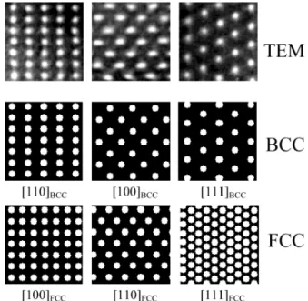
Obviously, the simulated bcc images match the TEM images better than the fcc images, when the TEM images are compared with the simulated bcc and fcc ones along the three [100], [110], and [111] zone axes, as is shown in Figure 7. Consequently, the mesostructure is determined to be bcc with a ) 13.0 nm and average diameter of the mesopores of 4 nm.
3.3. Further Investigation between bcc and bct.
Although the mesostructure was determined first as bcc, the discrepancy between the TEM and the simulated images is evident to a certain degree. To ascertain quantitatively the inconsistency, the values of the ex-perimental plane spacings (dhkl) are measured and com-pared with the corresponding theoretical ones. Various plane spacings (dhkl, nm) are obtained and presented in Table 2; they are d002from Figures 1-4, d020from Figure
2, d011from Figures 2 and 5, d110from Figures 3-5, and d101from Figure 5. These plane spacings (dhkl) are acquired
directly from the TEM images and from the diffraction patterns and are summarized in columns 3 and 4 as d1
and d2in Table 2, respectively. In addition, theoretical
values of dhkl(d3) are given correspondingly in column 5,
the values of which are from a bcc structure with a ) 13.0 nm using dhkl) a/(h2+ k2+ l2)1/2.
When the plane spacing (dhkl) is to be measured from the TEM image, a line profile intensity method is used for precision; image-processing software, so-called Image-Pro (Media Cybernetics, Inc.), was used. An example of this measurement is demonstrated in Figure 4d. In this line profile, the x axis gives the spatial scale (in pixels), while the y axis gives the average intensity (in an arbitrary unit); the intensity along a band from left to right between the two lines (indicated in Figure 4a) is plotted as a function of the distance (from left to right along the two lines). Each peak represents the position of a{110}plane: the thirteen peaks in Figure 4d come from the thirteen{110}
planes shown in Figure 4a. Accordingly, the averaged
{110}plane spacing (d110) can then be calculated as
where pland pfare the last and first peak positions (pixels),
respectively, while n is the number of peaks and m is the magnification. In the present study, the magnification for the TEM image (Figure 4a) is 34 600. Also, negative films are scanned with the resolution of 1350 pixels/in.; thus, m ) (2.54 × 10⁷)/(1350 × 34 600) ) 0.5438 nm/pixel.
As is shown in Figure 4d, pl) 211 pixels, pf) 8 pixels and
n ) 13. Thereby, d110) 9.2 nm is obtained.
When the plane spacing is to be obtained from the diffraction pattern, the relationship between a certain plane{hkl}spacing (dhkl) and the corresponding diffraction
spot is given by
where R is the distance between the diffraction spot (hkl) and the transmitted (central) spot (000); when the magnification factor is not one for a presented diffraction pattern, R should be divided by the factor number. L is the camera length, and λ is the wavelength of the electrons at the given accelerating voltage when the diffraction pattern is taken. λL is a constant under one operation and is the so-called camera constant.
For accuracy, the diffraction pattern of the Si wafer (Figure 1b) was employed to calibrate the camera constant (λL) with eq 3. The Si plane spacing dhklof the plane (hkl) can be obtained from dhkl) a/(h2+ k2+ l2)1/2, using the well-known Si lattice constant a ) 0.5431 nm; such Si has a diamond structure. Thus, the calibrated (λL)cis 69.6
mm Å, which is close to the calculated value 72.8 mm Å, with the camera length L ) 2900 mm and λ ) 0.0251 Å. The data presented as d2in Table 2 are calculated with
the calibrated camera constant (λL)c.
It is of interest to point out that the plane spacing d002
can also be attained from the diffraction pattern of Figure 1b. The four diffraction spots 002 and 0,0,-2 from Si and silica are considered; the simple distance ratio between Si(002) to (0,0,-2) and silica (002) to (0,0,-2) can be used to get the film d002.
Because of some divergence between the d3values and divalues (i ) 1-2) in Table 2, the mesostructure should not be perfectly bcc. Therefore, a bct structure is cautiously suggested. During the EISGSA processes as well as subsequent pyrolysis, tensile stresses that are biaxial can develop in thin films coated on substrates.13If a sol-gel
film is not attached to any substrate, there will be no stress because of the ability to freely shrink to its stress-free state. On the other hand, if the film is non-stress-free- non-free-standing but is constrained to a substrate, the shrinkage can only occur freely in the direction (z) perpendicular to the film/substrate interface (x-y plane). Accordingly, a bct mesophase seems to be more rational than a body-centered orthogonal one for the present slightly distorted bcc mesostructure because of the biaxial stress presented in the film. In addition, it seems logical to suggest a bct mesostructure with the lattice constant c smaller than a. Various values of a and c are considered in the comparison of bcc with bct; the plane spacing for a bct structure can be obtained from the following equation:
Among the tested values of a and c, the bct structure with
a ) 13.5 nm and c ) 13.0 nm seems sensible. The
theoretical dhkl (d4) of this bct structure are calculated
and presented correspondingly in column 6 in Table 2. In addition to the plane spacing, the angles φ between various planes are also considered in the determination of the slightly distorted bcc structure. The experimental values of φ are compared with those calculated from the theoretical bcc and bct structures. The experimental angles φ between two planes are measured directly from the different patterns (shown in Figures 1-5). The measured
(13) Lu, M.; Brinker, C. J. Unpublished results. The onset of the silica condensation takes place in the very late stage of the EISA process. Table 2. Plane Spacings (d, nm) Measured from the TEM
Images (d1) and Diffraction Patterns (d2), as Well as
Calculated Values under the Assumption of bcc (d3, with a ) 13.0 nm) and bct (d4, with a ) 13.5 nm and c ) 13.0
nm) figure planes d1 d2 d3 d4 1a,c 002 6.5 6.4 6.5 6.5 2a,b 6.3 6.4 3a,b 6.6 6.5 4a,b 6.7 6.6 2a,b 020 7.3 7.4 6.5 6.8 2a,b 011 9.3 9.4 9.2 9.4 5a,b 9.3 9.3 3a,b 110 9.3 9.3 9.2 9.5 4a,b 9.2 9.3 5a,b 9.6 9.7 5a,b 101 9.1 9.2 9.2 9.4 dhkl)pl- pf n - 1m (2) Rdhkl)λL (3) dhkl) 1
x
(h2+ k2)/a2+ (l/c)2 (4) MTES-Derived Silica Thin Film, Part 1 Langmuir, Vol. 19, No. 18, 2003 7287results φ1 are summarized in column 3 in Table 3. In
addition, columns 4 and 5 in Table 3 are the correspond-ingly calculated angles φ2and φ3, from the bcc structure
with a ) 13.0 nm (eq 5) and the bct structure with a ) 13.5 nm and c ) 13.0 nm (eq 6), respectively.
When the calculated values from the bcc and bct structures are compared with the experimental data shown in Tables 2 and 3, there is some discrepancy. From the various combinations of a and c tested, we suggest that the mesostructure is bct with a ) 13.5 nm and c ) 13.0 nm. Such a suggestion is supported especially from the comparison of φ2and φ3with φ1; the values of φ3seem
to be relatively close to those of φ1compared to the values
of φ3. Because of the presence of stress in the sol-gel and
calcination processes, it seems almost impossible to achieve a perfect bcc mesostructure. Accordingly, the present mesostructure is not perfectly bcc (with a ) 13.0 nm and a slight distortion) but rather bct (with a ) 13.5 nm and c ) 13.0 nm).
4. Conclusions
TEM was used to characterize the mesostructure of a self-assembled hydrophobic silica thin film with spherical voids arranged in an ordered array. A TEM approach was developed to resolve the mesostructure. This method involved sample tilting to get different zone axes, simula-tion, and calculation. The mesostructure was conclusively found to be slightly distorted bcc rather than fcc, and probably bct. This novel self-assembled MTES-derived silica thin film should be a promising candidate for low-dielectric-constant (k) insulating materials needed for future semiconductor devices.
Acknowledgment. We thank Dr. Celeste A. Drewien
for useful discussions.
Note Added after ASAP Posting. This article was
released ASAP on 8/6/2003 with an error in eq 4. The correct version was posted on 8/14/2003.
LA034310H cos φ ) h1h2+ k1k2+ l1l2
x
(h12 + k12+ l12)(h22+ k22+ l22) (5) cos φ ) (1/a2)(h1h2+ k1k2) + (1/c2)l1l2x
[(1/a2)(h 12+ k12) + (1/c2)l12][(1/a2)(h22+ k22) + (1/c2)l22] (6)Table 3. Angles O between Planes, with O1Measured
Directly from Diffraction Patterns and O2and O3
Calculated from the bcc (with a ) 13.0 nm) and bct (with
a ) 13.5 nm and c ) 13.0 nm) Mesostructures, Respectively figure planes φ1 φ2 φ3 2b 002; 020 88 90 90 2b 002; 011 40 45 44 2b 011; 020 48 45 46 2b 020; 0,1,-1 50 45 46 4b 002; -1,1,0 90 90 90 5b -1,0,1; -1,1,0 63 60 61 5b -1,1,0; 0,1,-1 60 60 61 5b 0,-1,1; -1,0,1 58 60 59
![Figure 2. Cross-sectional sample tilted 16° from that in Figure 1a with t 1 as the tilting axis: (a) the TEM image, (b) the diffraction pattern, and (c) indices for bcc [100].](https://thumb-eu.123doks.com/thumbv2/123doknet/14193751.478619/4.918.477.836.430.728/figure-cross-sectional-figure-tilting-diffraction-pattern-indices.webp)
![Figure 5. Scratched sample tilted 34° from the Figure 4 position with the t 2 as the tilting axis: (a) the TEM image, (b) the diffraction pattern, and (c) the indices for bcc [111].](https://thumb-eu.123doks.com/thumbv2/123doknet/14193751.478619/5.918.84.441.66.439/figure-scratched-figure-position-tilting-diffraction-pattern-indices.webp)