HAL Id: hal-03231064
https://hal.archives-ouvertes.fr/hal-03231064
Submitted on 20 May 2021HAL is a multi-disciplinary open access archive for the deposit and dissemination of sci-entific research documents, whether they are pub-lished or not. The documents may come from teaching and research institutions in France or abroad, or from public or private research centers.
L’archive ouverte pluridisciplinaire HAL, est destinée au dépôt et à la diffusion de documents scientifiques de niveau recherche, publiés ou non, émanant des établissements d’enseignement et de recherche français ou étrangers, des laboratoires publics ou privés.
Andreev reflection of fractional quantum Hall
quasiparticles
M. Hashisaka, T. Jonckheere, T. Akiho, S. Sasaki, J. Rech, T. Martin, K.
Muraki
To cite this version:
M. Hashisaka, T. Jonckheere, T. Akiho, S. Sasaki, J. Rech, et al.. Andreev reflection of fractional quantum Hall quasiparticles. Nature Communications, Nature Publishing Group, 2021, 12, pp.2794. �10.1038/s41467-021-23160-6�. �hal-03231064�
Andreev reflection of fractional quantum Hall quasiparticles
M. Hashisaka1,2,*, T. Jonckheere3, T. Akiho1, S. Sasaki1, J. Rech3, T. Martin3 & K. Muraki1 1 NTT Basic Research Laboratories, NTT Corporation, 3-1 Morinosato-Wakamiya, Atsugi,
Kanagawa 243-0198, Japan
2JST, PRESTO, 4-1-8 Honcho, Kawaguchi, Saitama 332-0012, Japan 3Aix Marseille Univ, Université de Toulon, CNRS, CPT, Marseille, France
*masayuki.hashisaka.wf@hco.ntt.co.jp
Abstract
Electron correlation in a quantum many-body state appears as peculiar scattering behaviour at its boundary, symbolic of which is Andreev reflection at a metal-superconductor interface. Despite being fundamental in nature, dictated by the charge conservation law, however, the process has had no analogues outside the realm of superconductivity so far. Here, we report the observation of an Andreev-like process originating from a topological quantum many-body effect instead of superconductivity. A narrow junction between fractional and integer quantum Hall states shows a two-terminal conductance exceeding that of the constituent fractional state. This remarkable behaviour, while theoretically predicted more than two decades ago but not detected to date, can be interpreted as Andreev reflection of fractionally charged quasiparticles. The observed fractional quantum Hall Andreev reflection provides a fundamental picture that captures microscopic charge dynamics at the boundaries of topological quantum many-body states.
When a two-dimensional electron system (2DES) is subjected to a perpendicular magnetic field at low temperatures, electrons condense into the strongly correlated phase of the fractional quantum Hall (FQH) state1. Quasiparticles in FQH systems have fascinating properties, such as fractional
charge2 and anyonic statistics3. Furthermore, for particular states such as that at Landau-level filling
factor v = 5/2, theory predicts that quasiparticles obey non-Abelian braiding statistics that provide the basis of fault-tolerant quantum computation4,5. The fractional charge6-9 and anyonic nature10-12 of the
quasiparticles have been revealed experimentally by shot-noise measurements and Fabry-Pérot interferometry. These studies have elucidated the behaviour of quasiparticles within the FQH state— either bulk or edges—that gives their defining properties. On the other hand, one may expect the quasiparticles to exhibit unique behaviour at an interface between the FQH state and another topologically distinct system, in a similar way as the Cooper-pair correlation in a superconductor manifests itself as Andreev reflection, where an electron incident from a normal metal to a superconductor is reflected as a hole13,14. This, in turn, poses a fundamental question as to whether
electron correlation in a topological quantum many-body state shows up as a unique interface phenomenon. FQH Andreev reflection, which we demonstrate in this paper, is an elementary process that answers this question.
The FQH Andreev process has been predicted by theories examining charge transport across a narrow junction between quantum Hall (QH) states with different filling factors. The most intensively studied system is one comprised of the v = 1/3 Laughlin state and the v = 1 integer QH (IQH) state15,16.
The charge transport can be modelled as the tunnelling between the v = 1/3 and 1 edge channels, which can be treated as a chiral Luttinger liquid and a Fermi liquid, respectively17. When the channels are
coupled through a single scatterer, the problem can be solved analytically by transforming it into that of tunnelling between edge states with Luttinger parameter g = 1/218,19. The exact solution predicts that
in the strong-coupling regime the two-terminal conductance G exceeds the conductance e2/3h (e:
electron charge, h: Planck’s constant) of the v = 1/3 state, reaching e2/2h in the strong-coupling
limit15,16,18-21. The enhancement of G can be interpreted as the result of the Andreev process, where
two incoming charge-e/3 quasiparticles are scattered into a transmitted electron with charge e and a reflected quasihole with charge e/315. This theoretical prediction, however, has not yet been
confirmed experimentally, despite recent progress in experiments on related systems22-26.
In this paper, we present evidence of the FQH Andreev process, namely G exceeding e2/3h in
a narrow junction between v = 1/3 and 1 states. As the junction width is varied using the split-gate voltage applied to form the junction, G oscillates around e2/3h, exhibiting several peaks where G
several Andreev processes at multiple scatterers present between the v = 1/3 and 1 edges. The evidence is also reinforced by demonstrating that the junction operates as a dc-voltage transformer generating a negative voltage output for positive input.
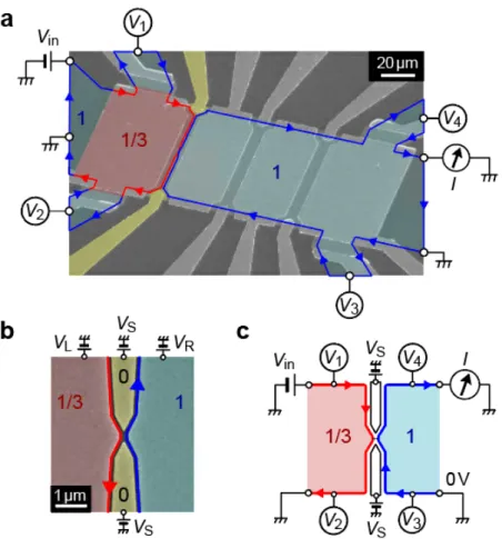
Figure 1 Fractional-integer quantum Hall junction. a-b, False-colour scanning electron
micrograph of the Hall-bar sample with measurement configurations (a) and magnified view near the narrow junction (b). A perpendicular magnetic field B = 9 T is applied from the back to the front of the sample. The v = 1 states develop over the wide blue regions in the 2DES with the front-gate voltages, including VR, set at 0 V. Meanwhile, electron density below one of the front gates (red
region) is reduced to form the v = 1/3 state by applying VL = 0.42 V. A narrow 1/3-1 junction is
formed by depleting the 2DES under the split gate electrodes (yellow) with negative VS. Chiral edge
states are displayed by arrows (blue, between v = 1 and v = 0; red, between v = 1/3 and v = 0). Vin is
the applied source-drain voltage, I is the measured current, and Vi (i = 1-4) are the measured voltages
of the incoming and outgoing channels of the 1/3-1 junction. c, Schematic of the experimental setup. A narrow junction is formed between v = 1/3 and v = 1 states.
Our QH device, formed in a Hall bar containing a 2DES in a GaAs quantum well, has several top gates and pairs of split gates in between (Fig. 1a). A perpendicular magnetic field of B = 9 T sets the bulk of the 2DES at v = 1. We then use the leftmost top gate (VL = 0.42 V) to form a v = 1/3 region
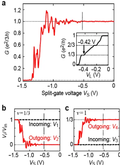
Figure 2 Signatures of Andreev reflection. a, Two-terminal conductance G as a function of
split-gate voltage VS, taken with VL = 0.42 V. Below VS 0.55 V (indicated by a dashed line), the
2DESs underneath the split gate electrodes are depleted to form a narrow 1/3-1 junction. Conductance oscillations with G > e2/3h, the evidence of the Andreev reflection, are observed.
(Inset) G as a function of leftmost top gate voltage VL measured with VS = 0, indicating that a v =
1/3 state forms at VL = 0.42 V in the region immediately to the left of the junction (red region in
Figs. 1a and 1b). b-c, VS dependence of the voltages on the incoming (V1 and V3) and outgoing (V2
and V4) channels, measured in the same setup as in a on the v = 1/3 (b) and v = 1 (c) sides of the
junction. The vertical axes are normalised by the source-drain voltage Vin. Both negative output (V2
< 0) in the reflected channel and overshoot (V4 > Vin/3) in the transmitted channel are the signatures
underneath (see the inset in Fig. 2a). A narrow 1/3-1 junction is formed by applying a negative gate bias VS to both electrodes of the split gate located immediately to the right of v = 1/3 region and
depleting the 2DES underneath (Fig. 1b). In this situation, the setup for transport measurements can be expressed schematically as in Fig. 1c [see Supplementary Note 1]. We measured the two-terminal differential conductance dI/dVin by applying a source-drain voltage Vin = Vindc + Vinac on the v = 1/3
side of the junction and measuring the transmitted current I on the v = 1 side using a standard lock-in technique.
Figure 2a presents the central result of this paper, where we plot the zero-bias conductance G, i.e., dI/dVin at Vindc = 0 V, as a function of VS. A narrow junction forms at VS < 0.55 V. As VS is
decreased below 0.55 V, the junction width decreases and G starts to oscillate around e2/3h with the
amplitude growing with decreasing VS. The most striking observation is that G overshoots e2/3h at
several oscillation peaks before the junction is pinched off at VS 1.4 V. The maximum G reaches
1.2 e2/3h at V
S 1.1 V. Such a two-terminal conductance, enhanced by narrowing the junction and
exceeding the conductance of the constituent element, is nontrivial and counter-intuitive. We note that these features appear only in 1/3-1 junctions and not in 1/3-1/3 or 1-3 junctions (see Supplementary Note 7).
The peculiarity of the charge-transfer process is revealed alternatively by probing the potentials, or voltages Vi (i = 1-4) of the incoming and outgoing edge channels. Figures 2b and 2c display Vi
measured at Vindc = 0 V normalized by Vin, plotted as a function of VS. The voltages V1 and V3 of the
incoming channels are, respectively, equal to potentials Vin and 0 V of the electrodes on their upstream,
independent of VS. In contrast, the voltages V2 and V4 of the outgoing channels vary with VS. The most
remarkable feature is the negative voltage that appears in V2. Phenomenologically, this demonstrates
that the junction operates as a dc-voltage transformer generating negative voltage output (V2 < 0) for
a positive input (Vin > 0).
From the Landauer-Büttiker formalism, V2 and V4 are related to G as
2
1 2 [1 / 3 ] in V G e h V , (1)
2
1 4 / 3 in V G e h V . (2)These formulas show that both V2 < 0 and V4 > Vin/3 correspond to G > e2/3h. Within the picture of
Andreev reflection, the negative voltage (V2 < 0) of the back-reflected channel is a direct manifestation
of the quasihole reflection.
While it is evident that the Andreev reflection is responsible for the observed G > e2/3h, to
which is not predicted from the original models based on the tunnelling through a single scatterer18,19.
Resonant tunnelling through unintentional discrete levels in the junction, which is responsible for the oscillations in the low-conductance regime near VS = 1.3 V (see Supplementary Note 4), cannot
account for the conductance oscillations with G > e2/3h. In the following, we present the dependence
of the conductance on Vin and temperature T and discuss the oscillation mechanism.
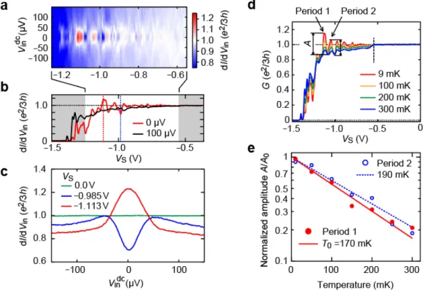
Figure 3a displays a colour plot of differential conductance dI/dVin as a function of VS and Vindc.
The oscillations with dI/dVin > e2/3h are seen only at |Vin| < 40 V. For illustration, we plot in Fig. 3b
the pinch-off trace at Vindc = 100 V, where dI/dVin < e2/3h over the entire range of VS. Figure 3c shows
Figure 3 Source-drain-voltage and temperature dependence of conductance oscillations. a,
Colour plot of dI/dVin as a function of VS and Vindc, indicating oscillations with dI/dVin > e2/3h at
|Vin| < 40 V.b, Comparison of dI/dVin vs VS traces at zero and finite bias, indicating that the feature dI/dVin > e2/3h is absent at Vindc = 100 µV. c, Vindc dependence of dI/dVin at several VS. Zero-bias
conductance enhancement (suppression) is observed at VS = 1.113 V (0.985 V), whereas no
feature is seen without forming a narrow junction (VS = 0 V). d, G vs. VS traces measured at several
temperatures. The amplitudes A of the oscillations in periods 1 and 2 are estimated as the peak-to-valley values. e, Temperature dependence of A/A0 for periods 1 and 2. The curves of the form
the Vindc dependence of dI/dVin at VS = 1.113 and 0.985 V. At VS = 1.113 (0.985) V, which
corresponds to the peak (valley) of the oscillations in Fig. 3b, we observe a pronounced zero-bias enhancement (suppression) of the conductance. In contrast, at VS = 0 V, where the v = 1/3 and 1 regions
form a long junction spanning across the 80-m-wide Hall bar, dI/dVin remains constant at e2/3h. These
results clearly show that the Andreev process is observed only in narrow junctions at low bias. The data also reveal that not only the conductance enhancement but also its suppression are low-bias anomalies.
Figure 3d shows the T dependence of the conductance oscillations. The oscillation amplitude decreases with increasing T, and the signature of the Andreev process, G > e2/3h, disappears above
200 mK. We focus on two single periods of the oscillations near VS = 1.113 and 1.095 V and extract
the amplitude A as the peak-to-valley value of G in each period. The two sets of A vs. T data are well fitted by an exponential function A0exp(T/T0), as shown in Fig. 3e, where A0 is the amplitude at T =
0 and T0 is the characteristic temperature. The exponential temperature dependence bears analogy with
that seen in various electronic interferometers27. The T0 values (170 and 190 mK) are close to each
other, indicating that these oscillations share the same origin in nature. The data in Fig. 3 also demonstrate that the conductance oscillations with G > e2/3h are highly reproducible (similar
conductance oscillations were reproduced for different cool-downs and in different samples, see
Supplementary Note 3, 5, and 6).
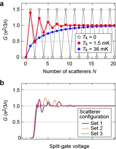
We argue that several Andreev processes in the junction are responsible for the conductance oscillations, as predicted in theories involving multiple scatterers or a line junction of finite width18,19,28-32. We consider N scatterers along the counter-propagating v = 1/3 and 1 channels and
incoherent transport between them. N is proportional to the junction width (i.e., length of the counter-propagating channels) and hence varies with VS. Here, “incoherent transport” means that the N
scatterers give independent scattering events, where the outgoing channels are characterized by a chemical potential that defines the input for the next scatterer. With this assumption the voltage of the
v = 1/3 (1) channel incoming to the nth scatterer is given by Vn1 = in1 × 3h/e2 (WNn = jNn × h/e2),
where in1 (jNn) is the current in the incoming channel. With this setup, one can use the exact solution
for the single-scatterer model19to define the conductance gn for each scatterer as a function of the
applied bias Vn1 WNn and evaluate the current In flowing through it. Notably, as shown for the
single-scatterer case, the charge conservation law and the requirement that the outgoing power be equal to or less than the incoming one lead to 0 ≤ gn ≤ 1/221. Here, the charge transport through the nth
strong-coupling limit (complete destrong-coupling). Namely, tunnelling for any intermediate gn values is
accompanied by energy dissipation.
The conductance G of the whole junction is obtained by solving a non-linear system of equations numerically. The results are shown in Fig. 4a for three representative cases: strong (Tk = 0,
black open circles), intermediate (Tk = 1.5 mK, red filled circles), and weak couplings (Tk = 36 mK,
blue diamonds) under the experimental condition with an applied voltage of 20 µV and a temperature of 9 mK. Here, Tk is the crossover energy scale between strong- and weak-coupling regimes19 (for
details, see Supplementary Note 8). In the strong-coupling limit, where we have gn = 1/2 for all n, each
scatterer only switches the sign of the voltage between the channels without causing energy dissipation.
Figure 4 Simulation of conductance oscillations using incoherent N scatterers model. a, N
dependence of G for several coupling strengths: strong-coupling limit (Tk = 0, black open circles),
intermediate (Tk = 1.5 mK, red filled circles), and weak couplings (Tk = 36 mK, blue diamonds). b,
Simulations taking the effects of the confining potential and the randomness in the positions of the scatterers into account. A window function was used to relate the split-gate voltage with the number and strength of scatterers (for details, see Supplementary Note 8). The three traces (1-3) are obtained for different configurations of the scatterers’ positions.
Consequently, G oscillates as a function of N between 0 (N even) and e2/2h (N odd) (black circles).
This oscillation can be regarded as the result of successive dissipationless Andreev processes, where the tunnel current switches direction at each scatterer without changing magnitude. When the coupling weakens to give gn < 1/2, each scatterer equilibrates the channels, which results in the reduced output
voltage at each scatterer and hence damping of the conductance oscillations (red circles). The damping is significant particularly for large N, where the channels experience equilibration many times. When the coupling weakens further to give gn < 1/3 for all n, the tunnel current flows only in one direction.
In this case, G monotonically increases with N, asymptotically approaching G = e2/3h30 (blue
diamonds). The simulation for the intermediate coupling (red circles) captures essential features of the experimental data in Fig. 2a. If we take into account more realistic experimental situations, including the confining potential of the split gate and randomness in the positions of the scatterers, the simulation can even better reproduce the experimental features (Fig. 4b). In the simulation, the confining potential controls the effective width of the junction by multiplying a position-dependent window function to the coupling strength of the scatterers, resulting in weaker coupling near the junction ends and hence reduced oscillation amplitude (for details, see Supplementary Note 8).
While the above multiple-scatterer model well explains the VS dependence of G, it still fails to
account for the observed Vin and T dependence. Since the model inherits the Vin and T dependence of
the conductance from the single-scatterer model18,19, which gives dI/dV
in as an increasing function of
Vin and T, it remains incapable of reproducing oscillations decaying with Vin or T. This, in turn, suggests
that coherent processes neglected in the above model, such as interference between successive scattering events33, play an important role. We speculate that constructive (destructive) interference of
tunnelling amplitudes can enhance (suppress) the coupling strengths of several scatterers in some range of VS. Indeed, a theory considering coherent interference predicts that a 1/3-1 junction with Coulomb
interaction shows conductance oscillations up to e2/2h as a function of the junction width28. In this
view, conductance enhancement or suppression at the extrema of the oscillations is partly due to the interference enhancement of the coupling. This picture explains why the oscillations appear only at low Vin and T. Furthermore, it helps to understand why the simulation for the weak-coupling regime
of the incoherent model can mimic the VS dependence of G at high Vin (Fig. 3b) or high T (Fig. 3d).
Finally, we discuss a related interesting issue, namely the mixing of the v = 1/3 and 1 edge modes expected for a wide junction. Counter-propagating v = 1/3 and 1 channels studied here is a basic setup in the model for the edge modes of the hole-conjugate v = 2/3 FQH state34. There, inter-channel
Coulomb interaction and disorder-assisted tunnelling govern the mixing of the channels and thus determine their fate in the low-temperature and long-channel limit. The conductance oscillations with
mixing process, namely the “mesoscopic fluctuation” predicted in Ref. 32, suggesting the presence of the neutral-mode physics of counter-propagating channels at the 1/3-1 junction31,32. Our findings
indicate that the Andreev process is a vital ingredient therein.
We have demonstrated FQH Andreev reflection, which is one of the essential concepts for understanding edge transport at the boundaries of topological quantum many-body systems. We expect to observe similar Andreev processes in various FQH junctions with different electronic systems, including non-quantum Hall systems such as normal metals and superconductors35,36.
Methods
Sample fabrication. We fabricated the sample in a 2DES in a GaAs quantum well of 30 nm width.
The centre of the well is located 190 nm below the surface. The sample was patterned using e-beam lithography for fine gate structures and photolithography for chemical etching, coarse metalized structures, and ohmic contacts formed by alloying Au-Ge-Ni on the surface.
Measurement setup. We set electron density in the 2DES at 2.2 1011 cm2 by applying a back-gate
voltage of 1.29 V at a refrigerator temperature of 9 mK, except for the data in Figs. 3d and 3e. A perpendicular magnetic field B = 9 T was applied from back to front of the sample. The lock-in measurements were performed with the ac modulation of Vinac = 20 V RMS at 31 Hz. The
experimental results demonstrated in the main text were obtained for the split-gate device with the opening of 300 nm. The data from the devices with wider apertures are available in Supplementary Note 6.
References
[1] Tsui, D. C., Stormer, H. L. & Gossard, A. C. Two-dimensional magnetotransport in the extreme quantum liquid. Phys. Rev. Lett. 48, 1559–1562 (1982).
[2] Laughlin, R. B. Anomalous Quantum Hall Effect: An Incompressible Quantum Fluid with Fractionally Charged Excitations. Phys. Rev. Lett. 50, 1395-1398 (1983).
[3] Wilczek, F. Magnetic Flux, Angular Momentum, and Statistics. Phys. Rev. Lett. 48, 1144-1146 (1982).
[4] Moore, G. & Read, N. Nonabelions in the fractional quantum Hall effect. Nucl. Phys. B 360, 362– 396 (1991).
[5] Nayak, C., Simon, S. H., Stern, A., Freedman, M. & Das Sarma, S. Non-abelian anyons and topological quantum computation. Rev. Mod. Phys. 80, 1083–1159 (2008).
[6] Martin, T. Noise in mesoscopic physics, in Nanophysics: coherence and transport (ed. Bouchiat, H., Gefen, Y., Guéron, S., Montambaux, G., & Dalibard, J.) 283-359 (Elsevier, 2005).
[7] Saminadayar, L., Glattli, D. C., Jin, Y., & Etienne, B. Observation of the e/3 Fractionally Charged Laughlin Quasiparticle. Phys. Rev. Lett. 79, 2526-2529 (1997).
[8] de-Picciotto, R., Reznikov, M., Heiblum, M., Umansky, V., Bunin, G. & Mahalu, D. Direct observation of a fractional charge. Nature 389, 162-164 (1997).
[9] Hashisaka, M., Ota, T., Muraki, K., & Fujisawa, T. Shot-Noise Evidence of Fractional Quasiparticle Creation in a Local Fractional Quantum Hall State. Phys. Rev. Lett. 114, 056802-1-5 (2015).
[10] Bartolomei, H., Kumar, M., Bisognin, R., Marguerite, A., Berroir, J.-M, Bocquillon, E., Plaçais, Cavanna, A., Dong, Q., Gennser, U., Jin, Y., and Fève, G. Fractional statistics in anyon collisions.
Science 368, 173-177 (2020).
[11] Nakamura, J., Fallahi, S., Sahasrabudhe, H., Rahman, R., Liang, S., Gardner, G. C., & Manfra, M. J. Aharonov–Bohm interference of fractional quantum Hall edge modes. Nat. Phys. 15, 563-569 (2019). [12] Nakamura, J., Liang, S., Gardner, G. C., & Manfra, M. J. Direct observation of anyonic braiding statistics. Nat. Phys. 16, 931-936 (2020).
[13] Andreev, A. F. Sov. Phys. JETP 19, 1228-1231 (1964).
[14] Tinkham, M. Introduction to Superconductivity (McGraw Hill, 1996).
[15] Sandler, N. P., Chamon, C. C. & Fradkin, E. Andreev reflection in the fractional quantum Hall effect. Phys. Rev. B 57, 12324-12332 (1998).
[16] Nayak, C., Fisher, M. P. A., Ludwig, A. W. W., & Lin, H. H. Resonant multilead point-contact tunneling. Phys. Rev. B 59, 15694-15704 (1999).
[17] Chang, A. M., Chiral Luttinger liquids at the fractional quantum Hall edge. Rev. Mod. Phys. 75, 1449-1505 (2003) and references therein.
[18] Chamon, C. C. & Fradkin, E. Distinct universal conductances in tunneling to quantum Hall states: The role of contacts. Phys. Rev. B 56, 2012-2025 (1997).
[19] Sandler, N. P., Chamon, C. C. & Fradkin, E. Noise measurements and fractional charge in fractional quantum Hall liquids. Phys. Rev. B 59, 12521-12536 (1999).
[20] Wen, X.-G. Phys. Rev. B 50, 5420-5428 (1994).
[21] Chklovskii D. B. & Halperin, B. I. Consequences of a possible adiabatic transition between v = 1/3 and v = 1 quantum Hall states in a narrow wire. Phys. Rev. B 57, 3781-3784 (1998).
[22] Roddaro, S., Paradiso, N., Pellegrini, V., Biasiol, G., Sorba, L., & Beltram, F. Tuning Nonlinear Charge Transport between Integer and Fractional Quantum Hall States. Phys. Rev. Lett. 103, 016802-1-4 (2009).
Nonequilibrated counterpropagating edge modes in the fractional quantum Hall regime. Phys. Rev.
Lett. 113, 266803-1-5 (2014).
[24] Cohen, Y., Ronen, Y., Yang, W., Banitt, D., Park, J., Heiblum, M., Mirlin, A. D., Gefen, Y., & Umansky, V. Synthesizing a v = 2/3 fractional quantum Hall effect edge state from counter-propagating
v = 1 and v = 1/3 states. Nat. Commun. 10, 1920-1-6 (2019).
[25] Maiti, T., Agarwal, P., Purkait, S., Sreejith, G. J., Das, S., Biasiol, G., Sorba, L., & Karmakar, B. Magnetic-field-dependent equilibration of fractional quantum Hall edge modes. Phys. Rev. Lett. 125, 076802-1-6 (2020).
[26] Lin, C., Eguchi, R., Hashisaka, M., Akiho, T., Muraki, K., & Fujisawa, T. Charge equilibration in integer and fractional quantum Hall edge channels in a generalized Hall-bar device. Phys. Rev. B 99, 195304-1-9 (2019).
[27] Yamauchi, Y., Hashisaka, M., Nakamura, S., Chida, K., Kasai, S., Ono, T., Leturcq, R., Ensslin, K., Driscoll, D. C., Gossard, A. C., & Kobayashi, K. Universality of bias- and temperature-induced dephasing in ballistic electronic interferometers. Phys. Rev. B 79, 161306(R)-1-4 (2009) and references therein.
[28] Ponomarenko, V. V. & Averin, D. V. Comment on “Strongly Correlated Fractional Quantum Hall Line Junctions”. Phys. Rev. Lett. 97, 159701-1 (2006).
[29] Zülicke U. & Shimshoni, E. Conductance oscillations in strongly correlated fractional quantum Hall line junctions. Phys. Rev. B 69, 085307-1-9 (2004).
[30] Nosiglia, C., Park, J., Rosenow, B., & Gefen, Y. Incoherent transport on the v = 2/3 quantum Hall edge. Phys. Rev. B 98, 115408-1-24 (2018).
[31] Kane, C. L., Fisher, M. P. A., & Polchinski, J. Randomness at the Edge: Theory of quantum Hall transport at filling v = 2/3. Phys. Rev. Lett. 72, 4129-4132 (1994).
[32] Protopopov, I. V., Gefen, Y., & Mirlin, A. D. Transport in a disordered v = 2/3 fractional quantum Hall junction. Annals. of Physics 385, 287-327 (2017).
[33] Yang, I., Kang, W., Pfeiffer, L. N., Baldwin, K. W., West, K. W., Kim, E.-A., & Fradkin, E. Quantum Hall line junction with impurities as a multislit Luttinger liquid interferometer. Phys. Rev. B
71, 113312-1-4 (2005).
[34] MacDonald, A. H. Edge states in the fractional-quantum-Hall-effect regime. Phys. Rev. Lett. 64, 220-223 (1990).
[35] Lee, G., Huang, K., Efetov, D. K., Wei, D. S., Hart, S., Taniguchi, T., Watanabe, K., Yacoby, A. & Kim, P. Inducing superconducting correlation in quantum Hall edge states. Nat. Phys. 13, 693–698 (2017).
Yamamoto, M., Bomze, Y., Tarucha, S., & Finkelstein, G. Supercurrent in the quantum Hall regime.
Science 352, 966-969 (2016).
Acknowledgements
The authors thank T. Ito, N. Shibata, and T. Fujisawa for fruitful discussions and H. Murofushi for technical support. This work was supported by Grants-in-Aid for Scientific Research (Grants No. JP16H06009, No. JP15H05854, No. JP26247051, and No. JP19H05603) and JST PRESTO Grant No. JP17940407.
Author contributions M.H. conceived the experiment. M.H., T.A., and S.S. fabricated the sample.
M.H. performed the measurement and analysed the data. T.J. and K.M. performed the simulations. M.H., T.J., and K.M. interpreted the results with help from J.R. and T.M. M.H. wrote the manuscript with help from T.J. and K.M. All authors discussed the results and commented on the manuscript.
Supplementary Information for
“Andreev reflection of fractional quantum Hall quasiparticles”
M. Hashisaka1,2, T. Jonckheere3, T. Akiho1, S. Sasaki1, J. Rech3, T. Martin3 and K. Muraki1
1NTT Basic Research Laboratories, NTT Corporation, 3-1 Morinosato-Wakamiya, Atsugi, Kanagawa
243-0198, Japan
2JST, PRESTO, 4-1-8 Honcho, Kawaguchi, Saitama 332-0012, Japan 3Aix Marseille Univ, Université de Toulon, CNRS, CPT, Marseille, France
Supplementary Note 1: Landauer-Büttiker edge transport picture
Supplementary Fig. 1 is a schematic of the experimental setup showing the whole of the Hall-bar device, where the blue and red arrows show the v = 1 and 1/3 edge channels, respectively. When the counter-propagating v = 1 and 1/3 channels are fully equilibrated at the wide junction across the Hall bar, a chiral one-dimensional channel of conductance 2e2/3h is formed at the junction, as shown by a black arrow. The channels incoming to the narrow junction do not experience equilibration with any other channels before impinging on it, because both bulk v = 1 and 1/3 states are insulating (incompressible). Therefore, the incoming voltages V1 and V3 correspond to the voltages of the
electrodes at their upstream. Actually, we observe V1 = Vin and V3 = 0 over the entire range of VS, as
shown in Figs. 2b and 2c. When the narrow junction has conductance g, the transmitted current I is given by I = g(V1 – V3) = gVin; hence, we find g = G. This justifies the picture in Fig. 1c. Resultantly,
the outgoing voltages V2 and V4 are expressed as V2 = Vin – I (3h/e2) = [1 G(e2/3h)1]Vin and V4 = I
(h/e2) = G(e2/h)1V
in, as described in the main text.
Supplementary Note 2: Longitudinal and vertical resistances of the two-dimensional electron system
Supplementary Fig. 2a shows the longitudinal (Rxx) and vertical (Rxy) resistances of the bulk
two-dimensional electron system (2DES) as a function of the perpendicular magnetic field B at the back-gate voltage VBG = 1.29 V. Supplementary Fig. 2b shows a colour plot of Rxx in the VBG-B plane.
The experimental results presented in the main text were obtained at B = 9.0 T and VBG = 1.29 V (ν
1), indicated by the dotted line in Supplementary Fig. 2a and the white circle in Supplementary Fig. 2b.
Supplementary Note 3: Asymmetric split-gate biasing
Supplementary Figs. 3a and 3b show the colour plots of G measured as a function of the gate voltages VS1 and VS2 independently applied to the upper and lower split-gate electrodes (see
Supplementary Fig. 3d). The two graphs show the same experimental results in different ranges: 0.9 ×
e2/3h ≤ G ≤ 1.1 × e2/3h in Supplementary Fig. 3a; 0 ≤ G ≤ 1.25 × e2/3h in Supplementary Fig. 3b. Whereas G = e2/3h at VS1 > 0.55 V and/or VS2 > 0.55 V, G deviates from e2/3h when both VS1 and
VS2 are below 0.55 V, because the 2DESs under the split-gate metals are depleted near 0.55 V. In
this area, we observe the conductance oscillations with G > e2/3h (shown in red in Supplementary Fig. 3a) that are the signatures of several Andreev processes. Some peaks and dips in the conductance oscillations are likely to appear parallel to either VS1 or VS2 axis [e.g. along the line (i) in
Supplementary Fig. 3b], suggesting that the number of scatterers in the junction decreases one by one with these gate voltages. Supplementary Fig. 3c shows G traces as a function of the split-gate voltages swept along the four lines in Supplementary Fig. 3b. We observe a variety of conductance oscillations that reflect the positions of scatterers in the 1/3-1 junction.
Supplementary Figure 2. a, Magnetic field dependence of Rxx and Rxy. b, Colour
Supplementary Note 4: Resonant tunnelling through discrete levels
While our experimental results can be well understood with the multiple-scatterer model, here we complement our discussion by excluding the possibility that the conductance oscillations originate from resonant tunnelling through unintentionally formed discrete levels. Such discrete levels could form when puddles of different filling factors exist near the junction1. First of all, the presence of a discrete level by itself cannot induce G > e2/3h, because in the absence of the Andreev process the conductance is upper-limited to e2/3h of the v = 1/3 region. Second, the increase in the oscillation amplitude with decreasing VS (Fig. 2a) is inconsistent with the VS dependence of the tunnel barrier
height that increases with decreasing VS. Third, when we independently sweep the split-gate voltages
VS1 and VS2 (Supplementary Fig. 3d), no features of resonant tunnelling are seen in the region of G >
0.8 × e2/3h (Supplementary Fig. 3a); the conductance peaks and dips are likely to appear parallel to either VS1 or VS2. This observation indicates that the position of the scatterers within the junction, not
the energy level, is essential. This contrasts with the conductance peaks near the pinch-off where G is well below e2/3h; they shift diagonally with the asymmetric biasing, which is the behaviour expected for resonant levels (see Supplementary Fig. 3b). Thus, we conclude that the conductance oscillations around G = e2/3h are not caused by the resonant tunnelling but by the Andreev processes in the multiple-scatterer system.
Supplementary Figure 3. a,b, Colour plots of G as a function of VS1 and VS2 in different G
ranges: 0.8 × e2/3h ≤ G ≤ 1.2 × e2/3h in a and 0 ≤ G ≤ 1.25 × e2/3h in b. c, Pinch-off characteristics of G obtained by the split-gate voltage sweeps along the dashed lines in b (horizontally shifted for clarity). d, Gate voltages VS1 and VS2 applied to the split gate.
Supplementary Note 5: Magnetic field dependence
We examined the B dependence of the pinch-off characteristics of the 1/3-1 junction. Supplementary Fig. 4a shows a colour plot of G in the VS-B plane. The conductance oscillations with
G > e2/3h are observed over the measured range of 8.8 T < B < 9.2 T, indicating the Andreev processes remain present with a slight change in B. Near VS = 1.113 V, G seems to oscillate as a function of B
showing G > e2/3h at several peaks (Supplementary Fig. 4b). The oscillating B dependence may be related to the Aharonov-Bohm interference between tunnelling amplitudes through different scatterers.
Supplementary Note 6: Different samples
The signature of the Andreev process, G > e2/3h, is observed not only in the split-gate device demonstrated in the main text, which has the split-gate opening of 300 nm, but also in other samples having wider openings. We examined two samples, one with 600 and the other with 900-nm openings, fabricated on the same wafer. Supplementary Fig. 5 shows the pinch-off characteristics of these samples. Like the 300-nm device, both of them show the conductance oscillations with G > e2/3h, manifesting the Andreev reflection. It is worth noting that their oscillation amplitudes are smaller than those for the 300-nm device, suggesting enhanced equilibration or weaker couplings due to strong negative VS in the wider samples.
Supplementary Figure 4. a, Colour plot of G as a function of VS and B. b, B dependence of G at VS =
1.113 V.
Supplementary Note 7: Transport properties of different quantum Hall junctions
It is instructive to look at the transport properties of other QH junctions having different sets of filling factors. Supplementary Fig. 6a shows the pinch-off characteristics of a junction between v = 1/3 states formed by applying the top-gate voltages VL = VR = 0.42 V at VBG = 1.29 V and B = 9 T. Note
that G never exceeds the conductance e2/3h over the entire range of VS. At VS > 0.55 V, where the
2DES under the split gate is not depleted, we observe G < e2/3h, which results from the enhanced backscattering through puddles of different filling factors. Below VS = 0.55 V, the conductance
through the narrow junction is maintained at G e2/3h down to V
S = 0.95 V. Below 0.95 V, it
decreases to zero, indicating that the junction is completely pinched off at VS 1.2 V. Supplementary
Fig. 6b displays another result obtained from an IQH junction between v = 1 and v = 3 states. The system was prepared by applying VL = 0.42 V at VBG = 1.29 V and B = 3 T. Likewise, in this case, G
decreases from e2/h to zero without showing G > e2/h over the entire range of VS. Thus, the signature
of Andreev reflection is neither observed for a junction between the same v = 1/3 states nor between different IQH states. This, in turn, clearly exhibits that the conductance oscillations with G > e2/3h, demonstrated in the main text, are responsible for the Andreev reflection at the 1/3-1 junction.
Supplementary Figure 6. a, VS dependence of G of junction between v = 1/3 states. b, VS
Supplementary Note 8: Theoretical discussion
The tunnelling problem through a single scatterer between v = 1/3 and v = 1 edge states has been studied and solved in the literature2. By using a Luttinger liquid representation for the edge states, one can show that this system can be mapped on a junction between two v = 1/2 edge states, which can be solved exactly using a refermionisation procedure. The total current through the junction, for a bias voltage Vin and temperature T, can be written as
𝐼 𝑉in, 𝑇, 𝑇k 𝑉in 𝑇ksinh in 𝐹 k, in , (1) where Tk parametrises the coupling strength of the scatterer, and
𝐹 𝑎, 𝑏 cosh cosh sinh 𝜓 𝜓 𝜓 𝜓 ,
(2) with ψ the digamma function.
The most important result is that the conductance of the junction is e2/2h in the strong-coupling limit (corresponding to Tk 0), and the effective quasiparticles in the transport process are collective
excitations with a charge e/2, which is different from the charge of the individual excitations existing at each edge. The fact that the conductance reaches e2/2h means that the output voltage on the v = 1/3 can be larger than the input one and can be understood in terms of Andreev reflection.
When the junction between the two edge states is wide, it cannot be modelled as a single scatterer, and a model with many scatterers can be used. While the problem becomes much more complicated, one regime where results can be obtained easily is the incoherent regime (we defined “incoherent” in the main text). There, all interference effects are neglected, and the current through a given scatterer depends only on the incoming voltage on the two edges. The incoherent multiple-scatterer model is illustrated in Supplementary Fig. 7 for the case of four scatterers. The voltages V1, …VN and W1, …WN
can be obtained by solving the non-linear system of equations for n = 1, …N:
𝑉 𝑉 𝐼 𝑉 𝑊 , 𝑇, 𝑇k, , (3)
𝑊 𝑊 𝐼 𝑉 𝑊 , 𝑇, 𝑇k, , (4)
where In is given by Eq. (1), and V0 and W0 are the incoming voltages. One can solve the Eqs. (3) and
(4) numerically to obtain the outgoing voltages VN and WN, or the output currents from the junction.
When the scatterers are weak, the system can be linearized and solved exactly by going to the continuum limit3. For the conductance as a function of the junction width, or the length L of the
counter-propagating channels, one obtains
𝐺 𝐿, 𝑙 ⁄ expexp / / , (5)
where l is an effective equilibration length, which is related to the coupling strength. This result shows that, in the regime of many weak scatterers, the conductance never goes above e2/3h, and it reaches this value on a length scale ~ l. This is the behaviour shown in Fig. 4a with the blue diamonds obtained from the numerical calculation (Tk = 36 mK). It is also the behaviour observed
experimentally, for the conductance as a function of the split-gate voltage at high Vin or T (where
oscillations are washed out), in Figs. 3b and 3d. A very different regime is obtained in the strong-coupling limit, where Tk,n go to zero to give gn = 1/2 for all n. There, G becomes e²/2h for an
odd N and 0 for an even N, as shown by the black open circles in Fig. 4a. Between these regimes, for scatterers strong enough, a typical behaviour is shown by the red filled circles in Fig. 4a (Tk = 1.5 mK),
namely, as a function of N, the conductance G oscillates around the value e²/3h, with G > e²/3h for odd
N, and G < e²/3h for even N. The amplitude of these oscillations decreases as N increases, and G
reaches eventually e²/3h for large N.
In the experiment, one does not have direct access to the number of scatterers. However, the number of scatterers should be roughly proportional to the junction width, which is controlled by the applied split-gate voltage VS. We model the continuous VS dependence of the conductance by making
the following reasonable assumptions:
- When no split-gate voltage is applied, the junction consists of a large number N, randomly placed inside the junction. In practice, we put 40 scatterers, with equal strength Tk, inside the range
[10,10] on the x-axis.
- The effect of VS is modelled as a window function which reduces the effective width of the
junction, with the strength of each scatterer going smoothly from Tk to ∞ (= zero-strength scatterer)
when the scatterer position goes from inside to outside the effective width determined by VS. In
practice, the strength of a given scatterer at position x is provided by the following function of VS:
𝑇 𝑉 , (6)
where f is a sigmoid function
𝑓 𝑦
exp ⁄ , (7)
where w defines the width of the transition region of the window function (in practice, we have chosen
w = 0.2). With this choice of window function, all scatterers are suppressed for negative VS
(corresponding to completely pinched-off junction), and the number of active scatterers increases as
VS increases, with all scatterers fully active when VS > 10.
Choosing a relatively strong coupling strength Tk = 1.1 mK, with an applied voltage 20 µV at
temperature 9 mK (for a single scatterer, these parameters give the conductance ~ 0.49 e²/h), we obtain the curves in Fig. 4b, each curve corresponding to a different random realization of the position of the scatterers. One can see that the major qualitative features of the experimental results are present; the amplitude of conductance oscillations around e²/3h decreases as VS is increased, while the
inherent oscillating pattern depends on the fine details of the positions of the scatterers.
Reference
[1] Baer, S., Rössler, C., de Wiljes, E. C., Ardelt, P.-L., Ihn, T., Ensslin, K., Reichl, C., & Wegscheider, W. Interplay of fractional quantum Hall states and localization in quantum point contacts. Phys. Rev. B
89, 085424-1-14 (2014).
[2] Sandler, N. P., Chamon, C. C. & Fradkin, E. Noise measurements and fractional charge in fractional quantum Hall liquids. Phys. Rev. B 59, 12521-12536 (1999).
[3] Nosiglia, C., Park, J., Rosenow, B., & Gefen, Y. Incoherent transport on the v = 2/3 quantum Hall edge. Phys. Rev. B 98, 115408-1-24 (2018).