HAL Id: hal-02373316
https://hal.sorbonne-universite.fr/hal-02373316
Submitted on 21 Nov 2019
HAL is a multi-disciplinary open access
archive for the deposit and dissemination of
sci-entific research documents, whether they are
pub-lished or not. The documents may come from
teaching and research institutions in France or
abroad, or from public or private research centers.
L’archive ouverte pluridisciplinaire HAL, est
destinée au dépôt et à la diffusion de documents
scientifiques de niveau recherche, publiés ou non,
émanant des établissements d’enseignement et de
recherche français ou étrangers, des laboratoires
publics ou privés.
Er/Yb-doped nanocrystals near gold nanodisks
Lionel Aigouy, Maria-Ujué González, Hung-Ju Lin, Mathilde
Schoenauer-Sebag, Laurent Billot, Patrick Gredin, Michel Mortier, Zhuoying
Chen, Antonio García-Martín
To cite this version:
Lionel Aigouy, Maria-Ujué González, Hung-Ju Lin, Mathilde Schoenauer-Sebag, Laurent
Bil-lot, et al..
Mapping plasmon-enhanced upconversion fluorescence of Er/Yb-doped nanocrystals
near gold nanodisks.
Nanoscale, Royal Society of Chemistry, 2019, 11 (21), pp.10365-10371.
ARTICLE
Received 00th January 20xx, Accepted 00th January 20xx DOI: 10.1039/x0xx00000x
Mapping Plasmon-Enhanced Upconversion Fluorescence of
Er/Yb-doped Nanocrystals Near Gold Nanodisks
Lionel Aigouy,*a Maria-Ujué González,b Hung-Ju Lin,a Mathilde Schoenauer-Sebag,a Laurent Billot,a Patrick Gredin,c Michel Mortier,c Zhuoying Chen,a and Antonio García-Martínb‡
Fluorescence enhancement effects have many potential applications in the domain of biochemical sensors and optoelectronic devices. Here, the emission properties of up-converting nanocrystals near nanostructures that support surface plasmon resonances have been investigated. Gold nanodisks of various diameters were illuminated in the near-infrared ( = 975 nm) and a single fluorescent nanocrystal glued at the end of an atomic force microscope tip was scanned around them. By detecting its visible fluorescence around each structure, it is found that the highest fluorescence enhancement occurs in a zone that forms a two-lobe pattern near the nanodisks and which corresponds to the map of the near-field intensity calculated at the excitation wavelength. In agreement with numerical simulations, it is also observed that the maximum fluorescence enhancement takes place when the disk diameter is around 200 nm. Surprisingly, this disk size is small when compared to that yielding the highest far-field scattering resonance, which occurs for disks with a diameter of 300-350 nm at the same excitation wavelength. This shift between the near and far-field resonances should be taken into account in the design of structures in systems that use plasmon enhanced fluorescence effects.
A. Introduction
Up-conversion luminescence is a process in which the emitted photons have a higher energy than the excitation ones. A typical illustration is rare-earth (RE) ions like Er3+, where two photons can be absorbed in the near-infrared (NIR) and re-emitted in the visible (VIS) range. This process involves several energy transfers between the real electronic levels of the different ions. The main drawback is that the two photon
absorption cross-section is weak1-3 compared to organic
molecules or inorganic quantum dots excited above their bandgap energy. In the case of RE-doped upconverting nanocrystals (UCN), one way to increase the efficiency is to couple them to metallic nanostructures that support a surface plasmon resonance (SPR). The intense and localized electromagnetic fields associated to the SPR can increase the NIR absorption and subsequently the fluorescence. The association of a plasmonic nanostructure and a UCN can find applications in several fields ranging from biological imaging to
optoelectronics.4-11 As an example, let us consider the case of
photovoltaic devices.12,13 For most solar cells, NIR photons are
lost because their energy is smaller than the bandgap of the material that absorbs the photons. Perovskite-based devices, which are promising candidates for manufacturing cheap and large scale solar cells, do not absorb light above 800 nm. This huge loss in solar energy could be partially compensated by the use of UCNs coupled to plasmonic structures. They could convert a fraction of NIR light into the VIS spectrum and therefore increase the solar cells responsivity window. Several studies have been recently performed on plasmon-induced fluorescence enhancements of RE-codoped UCNs. The coupling can be achieved by coating a metallic shell around the
nanocrystal4,8 or by dispersing the nanocrystals on a substrate
covered with metallic nanostructures. Using this configuration,
Wang et al.2 observed a 22-fold up-conversion fluorescence
enhancement near Ag nanostructures. Similarly, using a sharp
atomic force microscope (AFM) tip, Schietinger et al.14
approached an Er/Yb-doped nanocrystal near a gold nanosphere and observed a strong fluorescence increase compared to isolated nanocrystals. The enhancement can have several origins. It can be due to an increase of the local field at
the excitation wavelength9,13,15 and to an increase of the decay
rate at the emission one.15-17 Additionally, the numerous
energy transfers through the intermediate states of the RE ions (the up-conversion effect) may be influenced by the metallic nanostructures, either in a favorable or unfavorable manner, and this further complicates the underlying physics.9,18,19
In spite of recent investigations regarding plasmon-enhanced up-conversion,2,4,6-11,14,18,19 there is still a lack of knowledge and experimental work regarding the best relative position of
ARTICLE Journal Name
2 | J. Name., 2012, 00, 1-3 This journal is © The Royal Society of Chemistry 20xx
the UCN and the metallic nanostructure. Identifying the loci where the largest enhancement occurs is necessary to optimize the arrangement of the emitter/metal nanoparticle in devices such as solar cells. In contrast to previous studies, the aim of our work is to map the fluorescence enhancement near an isolated metal nanostructure. For that, we used an AFM tip on which a UCN is glued and, by scanning the tip over the nanostructure, we were able to map the up-conversion fluorescence. To better understand the relative importance of the effects that lead to enhancements, we simplified the situation to the study of elementary structures, namely circular gold nanodisks of different diameter, for which the interpretation of the results is feasible. We will show that the measured fluorescence maps present localized lobes that are qualitatively in good agreement with the calculation of the electromagnetic field intensity above the nanodisks at the excitation wavelength. We also observed that the intensity of the fluorescence lobes is maximum for disks having a diameter close to 200 nm and that it decreases with increasing disk sizes. Unexpectedly, at our excitation wavelength, numerical calculations show that the maximum of scattering or absorption should occur for disks with a 300-350 nm diameter. We reconcile the two findings by noting the existence of a spectral shift between the near-field maximum and the
far-field one,20-23 where the far-field scattering resonance
wavelength (SCA) is smaller than the near-field resonance one.
This effect, corroborated by our numerical simulations, should
also be taken into account when designing plasmonic nanostructures for fluorescence enhancement.
B. Experiments and simulations on a 200 nm large
structure
Mapping the loci of fluorescence enhancements near nanostructures can be done either by covering the whole surface with fluorescent material or by scanning a single fluorescent particle glued at the end of an AFM tip. The
resolution of the first technique is limited to /2 ( 500 nm at
our excitation wavelength) but the second can overcome this limit provided the fluorescent particle is sufficiently small. We
used a single KY3F10 nanocrystal (diameter between 80 and 150
nm) codoped with Er and Yb ions as fluorescent emitters. It was glued at the end of a sharp tungsten tip and placed on a homemade scanning near-field optical microscope (SNOM) /
AFM set-up.24,25 The metallic nanostructures were 60 nm-thick
Au nanodisks fabricated by e-beam lithography on a SiO2
substrate. Their diameter varied between 150 nm and 350 nm with an increasing step of 50 nm. In the following, the structures will be further referred as D150, D200, D250, D300 and D350. They were organized in arrays separated by 3 µm to avoid any near-field coupling. We show in Fig. 1 the experimental configuration of the SNOM/AFM set-up, a scanning electron microscope (SEM) image of sample D200, a SEM image of an example of tip, and the energy band diagram of the fluorescent nanocrystals with the multiple absorption and emission lines. Illumination comes from the rear face of the sample from a linearly polarized laser diode (EXC = 975
nm). The excitation is absorbed by Yb ions and transferred to adjacent Er ions. Due to large number of energy levels, several channels are possible between the different levels and the
ions.1 The up-conversion fluorescence is detected in the
525-560 nm spectral range, corresponding to the transitions
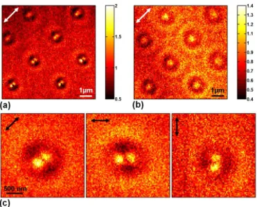
Figure 2: Fluorescence images measured at h1 = 0 nm (a) and h2 = 250 nm (b) above the 200 nm-diameter nanodisks (D200). Fluorescence images measured at h1 above one of these disks for different incident polarization directions (c).
Figure 1: Sketch of the illumination configuration and the scanning mode, the tip moves in an horizontal plane at h = 0 nm above the disks (a), SEM image of a 200 nm-large gold nanodisk array (b), emission spectrum of a nanocrystal when excited at EXC = 975 nm (c), SEM image of a typical tip with a fluorescent nanocrystal attached at the end (d), sketch of the energy bands and the transitions for an Er/Yb-doped nanocrystal when excited at EXC = 975 nm (e).
2
H11/24I15/2 and 4S3/24I15/2 which are the most intense
emission lines.
The fluorescence maps measured on D200 at two different heights above the structures are shown in Fig. 2. To avoid any alteration of the probe, the scans were made in a non-contact mode with the feedback loop disabled. Due to a slight non-parallelism between the sample and the scanning plane, the probe moves progressively away from the surface. For the
scan performed at h1 = 0 nm (Fig.2a), h being the distance
between the surface of the disk and the probe, an increase of fluorescence is observed above each nanodisk. The enhancement zone forms a two-lobe pattern, oriented in the incident polarization direction. A dark and bright ring is also visible around the lobes, showing that fluorescence is successively reduced and enhanced when the UCN is getting away from the disk. When the tip drifts away from the surface (top part of Fig. 2a), the two lobes tend to merge and form a
single elongated spot. At h2 = 250 nm (Fig. 2b), the pattern is a
circular spot bounded by the dark and bright rings and the two lobes disappear. In Fig. 2c, we show a series of fluorescence
images obtained at h1 for several incident polarization
directions. The orientation of the lobes rotates with the polarization of the excitation light. The dark and bright rings on the lobes side also rotate in the same manner.
Using a finite difference time domain (FDTD) method, we next
calculated the near-field intensity (ǁEǁ2) with a proprietary
code Lumerical®, which provides a robust and reliable solver for Maxwell’s equations. We use an impinging plane wave, of unit amplitude everywhere, from the glass side employing scattering-like boundary conditions (perfectly matching conditions in a simulation box ten times the diameter of the largest nanodisk, where the total field is contained in a box six times the diameter of the largest nanodisk and twenty its height (ten times above and ten times below). The mesh surrounding the nanodisk is set to be smaller than 5nm x 5nm x 2nm (width-depth-height) in a box three times the diameter and five the height of the largest nanodisk, uniformly growing to a maximum of 20nm x 20nm x 20nm uniform cubic mesh outside that box. The total field is then collected to give rise to
the near field intensity color maps. All are normalized to the impinging plane wave (unit amplitude for convenience). The corresponding numerical simulation for D200, shown in Fig. 3,
was performed in a plane situated at hS = 8 nm above the disk.
Although the up-conversion fluorescence is not linear with the incident power, [1,26-28] we limited the calculation to the near-field intensity, to simplify the analysis. As in the fluorescence experiment, two lobes are visible on the simulations (Fig. 3a), aligned in the direction of polarization of the excitation beam. In Fig. 3b and 3c, we took into account the size of the UCN by
integrating the intensity above hS over a 50 nm and 100
nm-large cube respectively. The lobes are ennm-larged, and the simulated images show the same characteristics as the fluorescence: same dark zones on the lobe’s sides, same bright ring situated 1 µm away from the disk. Increasing the width of the integration cube up to 150 nm did not change a lot the near-field map. The integration width of 100 nm is in agreement with the size of the UCN we use. Note that a similar two-lobe structure has already been observed around Au or Ag
nanostructures using a scattering SNOM.29-31But the contrast
mechanisms are completely different from one method to the other, one involving directly the scattering of the near-field, the other one involving the fluorescence induced by this near-field. At first sight, the observed good qualitative agreement with the simulation shows that the measured fluorescence is directly linked to the near-field intensity above the disks, at
EXC. However, a question that is raised concerns the influence
Figure 3: Near-field intensity calculated at hS = 8 nm above the disk with no average (a), integration on a 50 nm-wide cube above hS (b), integration on a 100 nm-large cube above hS (c). The excitation is polarized as indicated by the white arrow. The red square above the dashed lines represents schematically the integration zone, starting at hS above the disk surface.
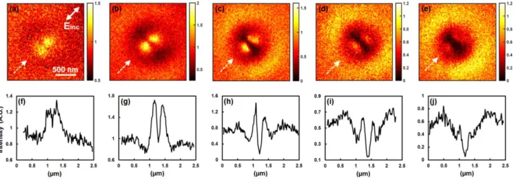
Figure 4: Fluorescence maps of isolated nanodisks (a,b,c,d,e), and cross-sections extracted from the fluorescence maps (f,g,h,i,j). The disk diameter are 150 nm (a,f), 200 nm (b,g), 250 nm (c,h), 300 nm (d,i) and 350 nm (e,j).
ARTICLE Journal Name
4 | J. Name., 2012, 00, 1-3 This journal is © The Royal Society of Chemistry 20xx
of the Au nanodisk on the emission process and in particular
on the emission rate and the quantum efficiency.15,16,32 Due to
the large number of evanescent modes at the resonance, the local optical density of states (LDOS) increases, which raises the radiative decay rate and results in fluorescence enhancement. However, we think that, although certainly present, this effect is not dominant in our experiments for this structure. Indeed, there is a mismatch between the emission line (525 - 560 nm) and the SPR of the nanodisk (> 650 nm for this size) which limits the LDOS. In addition, as will be discussed later, another possibility is that only the emitters located at short distance from the disk (for instance < 20 nm) undergo a change in the decay rate. But the overall contribution of all the ions inside the nanocrystal tends to lower the importance of such emission effect in comparison with the one due to the up-conversion excitation.
C. Influence of the disk size on the fluorescence
enhancement
The experiments shown in Fig. 2 were performed on disk D200. In order to assess in which manner the two-lobe pattern and the fluorescence enhancement depend on the nanostructure size, we also measured the fluorescence maps on disks D150 to D350. Experiments, shown in Fig. 4, were performed with the same tip, in the same experimental
conditions. We observe that all structures exhibit both the
two-lobe pattern very close to their center and the bright ring situated at a larger distance from the center of the disks. Let us first consider the bright rings around the disks. Their intensity increases with increasing disk size, particularly on the opposite sides of the near-field lobes, in the direction perpendicular to the incident polarization. This ring pattern looks like the well-known dipolar scattering pattern but here it is measured at short distance from their source, at the beginning of the far-field zone. Let us now consider the evolution of the two-lobe pattern located near the structures. The maximum fluorescence enhancement is observed on D200, and the lobes intensity decreases when increasing the disk size up to D350. Such loss of fluorescence at the position
of the lobes cannot be attributed to a gradual deterioration of the tip since the scans were not performed in the order of the disk size and also the same behavior was observed with several tips (see supplementary material).
To explain the reduction of fluorescence near the disks with increasing size, we first calculated by FDTD the near-field intensity for D200 and D350 in the plane parallel to the surface and situated at hS = 8 nm above them (see Fig. 5). Again, to
take into account of the UCN size, the intensity was integrated
on a 100 nm-large cube above hS. Like for D200, the simulation
on D350 shows the presence of two near-field lobes and a far-field lateral ring, but compared to the far-far-field lateral rings, the two lobes are more intense than the ones observed
experimentally.However, as indicated by the color scale, the
intensity of these lobes is smaller than the ones of D200 (the
maximum is 3 for D350 and 4.5 for D200). Then we next
calculated the near-field intensity in a plane perpendicular to the surface, above the disks, in the direction of the incident polarization (see Fig. 5c and 5d). In that case, for the sake of clarity, the intensity was not integrated on the particle volume. From these simulations, we see that the near field for D350 seems more localized near the surface than for D200, but undoubtedly it is also less intense.
Several explanations can be found regarding the difference in the contrast of the lobes between the experiment and the simulation for D350. Firstly, the integration over a cube may not have been the most accurate because it gives the same weight to ions located in the lower and the higher part of the UCN. A spherical or pyramidal shape could have been more appropriate. Secondly, without considering the shape, the strong localized field for D350 implies that the ions located in the lower part of the UCN should contribute the most efficiently to the fluorescence. But these ions may also be very sensitive to other effects not taken into account in the
Figure 5: Near-field intensity calculated above D350 (a,c) and D200 (b,d). The simulation are performed in a plane parallel to the surface at hS = 8 nm (a,b) or in a plane perpendicular to the surface (c,d). The intensity was averaged on a 100 nm wide cube for (a) and (b). No average was made for (c) and (d). The insets represent the experimental images.
Figure 6: Scattering spectra of individual nanodisks calculated by FDTD. Our excitation wavelength EXC is closer to the resonance wavelength of D350 (FF-D350) than the one of D200 (FF-D200). Nevertheless, the near-field fluorescence enhancement is larger for D200.
simulations. The presence of metal creates non-radiative decay channels that enhance the non-radiative decay rate and
quench the fluorescence.15,33,34 In addition, in the present case
of RE-ions excited by up-conversion, the energy transfer rates between different ions Yb3+ Er3+ and Er3+ Er3+ (Förster
energy transfers) and also within a single Er3+ ion (excited state
absorption) may also be influenced by the metal,
advantageously or not.17-19,35-37 The distance below which the
metal influences the decay rates and may quench the energy transfers strongly depends on the structure, and distances
going from a few nanometers15,38-40 to tens of nanometers
were reported recently.41 Therefore it is likely that
non-radiative energy transfers occur in our case and may be partly responsible for the lower fluorescence enhancement in the case of D350 compared to the simulation. However, the physical picture is well captured, since, whatever the difference of contrast, it remains that when increasing the disk size, both the fluorescence and the simulation maps exhibit an overall decrease of fluorescence.
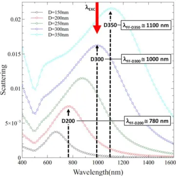
We next tried to correlate the intensity of the fluorescence to the plasmon resonance of the disks. For that, we calculated the evolution of the scattering spectra as a function of the disk size (see Fig. 6). They were obtained by integrating the Pointing vector normal to the surface plane, for the scattered field only, over an area covering a solid angle of 45º and
normalized to the source intensity. As previously reported,42
the resonance wavelength increases with increasing diameter.
Here, the excitation wavelength EXC (975 nm) matches the
far-field scattering resonance of disks D300 and D350 (FF-D300
1000 nm and FF-D350 1100 nm). Conversely, the resonance of
disk D200 (FF-D200 780 nm) is clearly not attuned to EXC.
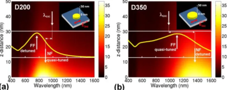
Even so, the near-field fluorescence enhancement is larger for D200 than for D300 or D350. We verified this behavior by calculating the near-field intensity at the corner of the disk for
D200 and D350 as a function of and for different heights
above the corner (see Fig. 7). For D200, the wavelength NF-D200
at which the near-field intensity reaches its maximum is close to 900 nm, a value which is red-shifted from the far-field resonance but which is not very far from the excitation wavelength. On the other hand, for D350, the near-field
resonance occurs at a wavelength NF-D350 (close to 1400 nm),
300 nm red-shifted from the far-field resonance and from our
excitation wavelength.These shifts between the near and
far-field resonances have recently been put forward both
theoretically and experimentally.20-23 An explanation for has
been given in Ref. 20 where the authors compare the dipolar plasmon resonance to a damped harmonic oscillator. The near-field amplitude is linked to the oscillation amplitude of the oscillator. Its maximum NF is spectrally shifted from the
far-field absorption and extinction peak o (which are linked to
the dissipation and to the kinetic energy) because of the
presence of the damping parameter . For nanostructure
diameters smaller than 100 nm, the shift is only of a few nanometers, increasing for larger structures like ours, where damping and retardation effects are relevant. Here, we find that for D200 and D350, the shifts are around 90 nm and 300 nm respectively. Finally, from the spectra of Fig. 6, it is
important to note that, in addition to the increment of the red shift of the far-field resonance with growing size, the intensity of scattering also increases. This is evident in the fluorescence maps of Fig. 4 where the intensity of the dipolar ring, oriented in the direction perpendicular to the incident polarization, increases as a function of the disk size.
It should be mentioned that, in the whole analysis presented here, we neglected the influence of the probe and the UCN on the measurements. It is well known that the SPR of a metallic
nanoparticle depends on the environment.43 However,
although such perturbation probably exists, we believe it would not cause an additional shift of the resonances since the size of the nanocrystal is relatively small compared to the size of the disk so that it does not cover its whole surface. In addition, previous studies performed with similar tips on the observation of surface plasmon polariton waves did not showed a significant perturbation of the local electromagnetic fields.44
Conclusions
We conducted an experimental study of the influence of gold
nanodisks on the up-conversion fluorescence of Er3+-doped
nanocrystals. We visualized where the fluorescence
enhancements occur near the structures and observed a two-lobe pattern aligned with the polarization direction of the excitation beam. This pattern corresponds to the intensity of
the near-field at the excitation wavelength. The agreement
with numerical simulations is very good, in particular for small diameters (200 nm). We observed that when increasing the disk size, the fluorescence enhancement decreases, although the associated far-field scattering resonance approached the excitation wavelength. Our numerical simulations suggested that the origin is in the presence of a spectral shift between the near-field and the far-field resonance of several hundreds of nanometers. Our study shows that, for practical applications where the highest up-conversion fluorescence enhancements is required, e.g. in solar cells, the design of structures has to be made by considering the spectral position and characteristics of the near-field resonance, rather than the far-field one.
Conflicts of interest
There are no conflicts to declare.
Figure 7: Near-field intensity calculated above the corner of D200 (a) and D350 (b) as a function of the wavelength and at an altitude that varies between z = 5 nm and z = 50 nm. The yellow curves are the far-field scattering spectra of the two disks.
ARTICLE Journal Name
6 | J. Name., 2012, 00, 1-3 This journal is © The Royal Society of Chemistry 20xx
Acknowledgements
The authors thank the support from the DIM Nano-K program from “Région Ile de France”, from the Idex Paris Sciences &
Lettres through the grant ANR-10-IDEX-0001-02 PSL,and from
the CNRS and the CSIC through the Spanish-French program PICS (grant SolarNano #PICS07687 and #PIC2016FR2).
References
1 F. Auzel, Chem. Rev., 2004, 104, 139.
2 Y.-L. Wang, N. M. Estakhri, A. Johnson, H.-Y. Li, L.-X. Xu, Z. Zhang, A. Alù, Q.-Q. Wang and C.-K. Shih, Scientific Reports, 2015, 5, 10196.
3 J.-C. Boyer and F. C. J. M. Van Veggel Nanoscale, 2010, 2, 1417.
4 P. Yuan, Y. H. Lee, M. K. Gnanasammandhan, Z. Guan, Y. Zhang and Q.-H. Xu, Nanoscale 2012, 4, 5132.
5 P. Kannan, F. A. Rahim, R. Chen, X. Teng, L. Huang, H. Sun and D.-H. Kim, ACS Applied Materials & Interfaces 2013, 5, 3508.
6 P. Wang, Z. Li, W. J. Salcedo, Z. Sun, S. Huang and A. G. Brolo,
Physical Chemistry Chemical Physics 2015, 17, 16170.
7 H. Zhang, Y. Li, I. A. Ivanov, Y. Qu, Y. Huang and X. Duan,
Angewandte Chemie International Edition 2010, 49, 2865.
8 L. Sudheendra, V. Ortalan, S. Dey, N. D. Browning and I. M. Kennedy, Chemistry of Materials 2011, 23, 2987.
9 D. M. Wu, A. Garcia-Etxarri, A. Salleo and J. A. Dionne, J.
Phys. Chem. Lett. 2014, 5, 4020.
10 A. C. Atre, A. García-Etxarri, H. Alaeian and J. A. Dionne,
Journal of Optics 2012, 14, 024008.
11 M. He, X. Pang, X. Liu, B. Jiang, Y. He, H. Snaith and Z. Lin,
Angewandte Chemie 2016, 128, 4280.
12 T. Trupke, M. A. Green and P. Würfel, Journal of Applied
Physics 2002, 92, 4117.
13 J. C. Goldschmidt and S. Fischer, Advanced Optical Materials 2015, 3, 510.
14 S. Schietinger, T. Aichele, H.-Q. Wang, T. Nann and O. Benson, Nano Letters 2010, 10, 134.
15 P. Anger, P. Bharadwaj and L. Novotny, Physical Review
Letters 2006, 96, 113003.
16 S. Kühn, U. Håkanson, L. Rogobete and V. Sandoghdar,
Physical Review Letters 2006, 97, 017402.
17 S. Fischer, D. Kumar, F. Hallermann, G. V. Plessen and J. C. Goldschmidt, Optics Express 2016, 24, 460.
18 Q.-C.Sun, H. Mundoor, J. C. Ribot, V. Singh, I. I. Smalyukh and P. Nagpal, Nano Letters 2013, 14, 101.
19 D. Lu, S. K. Cho, S. Ahn, L. Brun, C. J. Summers and W. Park,
ACS Nano 2014, 8, 7780.
20 J. Zuloaga and P. Nordlander, Nano Letters 2011, 11, 1280. 21 F. Moreno, P. Albella and M. Nieto-Vesperinas, Langmuir
2013, 29, 6715.
22 P. Alonso-González, P. Albella, F. Neubrech, C. Huck, J. Chen, F. Golmar, F. Casanova, L. E. Hueso, A. Pucci, J. Aizpurua and R. Hillenbrand, Physical Review Letters 2013, 110, 203902. 23 A. Cacciola, M. Iatì, R. Saija, F. Borghese, P. Denti, O. Maragò
and P. Gucciardi, Journal of Quantitative Spectroscopy and
Radiative Transfer 2017, 195, 97.
24 A. Vitrey, L. Aigouy, P. Prieto, J. M. García-Martín and M. U. González, Nano Letters 2014, 14, 2079.
25 L. Aigouy, A. Cazé, P. Gredin, M. Mortier and R. Carminati,
Physical Review Letters 2014, 113, 076101.
26 For these nanocrystals, we experimentally measured fluorescence intensities varying with a power law of 1.5 to 2 with the incident laser power. On such nanocrystals, the non-linear behaviour is difficult to infer due to saturation
effects that can also occur at moderate power. Due to the complexity of these power dependences, we decided to compare the fluorescence maps to the intensity of the near-field, as if the fluorescence was linear with the incident power.
27 H. P. Paudel, L. Zhong, K. Bayat, M. F. Baroughi, S. Smith, C. Lin, C. Jiang, M. T. Berry and P. S. May, The Journal of
Physical Chemistry C 2011, 115, 19028.
28 Dong, L.-D. Sun and C.-H. Yan, Nanoscale 2013, 5, 5703. 29 A. García-Etxarri, I. Romero, F. J. G. D. Abajo, R. Hillenbrand
and J. Aizpurua, Physical Review B 2009, 79, 125439. 30 R. Esteban R. ogelgesang . orfm ller . mitrie .
Rockstuhl, C. Etrich and K. Kern, Nano Letters 2008, 8, 3155. 31 M. Rang, A. C. Jones, F. Zhou, Z.-Y. Li, B. J. Wiley, Y. Xia and
M. B. Raschke, Nano Letters 2008, 8, 3357.
32 D. Cao, A. Cazé, M. Calabrese, R. Pierrat, N. Bardou, S. Collin, R. Carminati, V. Krachmalnicoff and Y. D. Wilde, ACS
Photonics 2015, 2, 189.
33 G. P. Acuna, M. Bucher, I. H. Stein, C. Steinhauer, A. Kuzyk, P. Holzmeister, R. Schreiber, A. Moroz, F. D. Stefani, T. Liedl, F. C. Simmel and P. Tinnefeld, ACS Nano 2012, 6, 3189. 34 G. Schneider, G. Decher, N. Nerambourg, R. Praho, M. H. V.
Werts and M. Blanchard-Desce, Nano Letters 2006, 6, 530. 35 W. Park, D. Lu and S. Ahn, Chemical Society Reviews 2015,
44, 2940.
36 R. Esteban, M. Laroche and J.-J. Greffet, Journal of Applied
Physics 2009, 105, 033107.
37 L. Zhao, T. Ming, L. Shao, H. Chen and J. Wang, The Journal of
Physical Chemistry C 2012, 116, 8287.
38 A. L. Feng, M. L. You, L. Tian, S. Singamaneni, M. Liu, Z. Duan, T. J. Lu, F. Xu and M. Lin, Scientific Reports 2015, 5, 7779. 39 Q. Luo, Y. Chen, Z. Li, F. Zhu, X. Chen, Z. Sun, Y. Wei, H. Guo,
Z. B. Wang and S. Huang, Nanotechnology 2014, 25, 185401. 40 X. Liu and D. Y. Lei, Scientific Reports 2015, 5, 15235.
41 W. Ge, X. R. Zhang, M. Liu, Z. W. Lei, R. J. Knize and Y. Lu,
Theranostics 2013, 3, 282.
42 W. A. Murray and W. L. Barnes, Adv. Mater. 2007, 19, 3771. 43 J. J. Mock, D. R. Smith and S. Schultz, Nano Letters 2003, 3,
485.
44 C. H. Gan, L. Lalouat, P. Lalanne and L. Aigouy, Physical