HAL Id: tel-00585601
https://tel.archives-ouvertes.fr/tel-00585601
Submitted on 13 Apr 2011
HAL is a multi-disciplinary open access archive for the deposit and dissemination of sci-entific research documents, whether they are pub-lished or not. The documents may come from teaching and research institutions in France or abroad, or from public or private research centers.
L’archive ouverte pluridisciplinaire HAL, est destinée au dépôt et à la diffusion de documents scientifiques de niveau recherche, publiés ou non, émanant des établissements d’enseignement et de recherche français ou étrangers, des laboratoires publics ou privés.
Nanoscale engineering of semiconductor heterostructures
for quadratic nonlinear optics and multiphoton imaging
Marcin Zieliński
To cite this version:
Marcin Zieliński. Nanoscale engineering of semiconductor heterostructures for quadratic nonlinear optics and multiphoton imaging. Other [cond-mat.other]. École normale supérieure de Cachan - ENS Cachan, 2011. English. �NNT : 2011DENS0005�. �tel-00585601�
Ecole Normale Supérieure de Cachan
Laboratoire de Photonique Quantique et Moléculaire
THÈSE DE DOCTORAT
Spécialité: Sciences Physiques et Chimiques
par
M
ARCINZ
IELIŃSKIpour obtenir le grade de Docteur de L’Ecole Normale Supérieure de Cachan
Le 9 Février 2011
NANOSCALE ENGINEERING OF SEMICONDUCTOR
HETEROSTRUCTURES FOR QUADRATIC NONLINEAR
OPTICS AND MULTIPHOTON IMAGING
Composition du jury:
M. BENOIT BOULANGER Président du jury M. HERVÉ RIGNEAULT Rapporteur M. LIBERATO MANNA Rapporteur M. DAN ORON Examinateur
M. DOMINIQUE CHAUVAT Codirecteur de thèse M. JOSEPH ZYSS Directeur de these
Institut d’Alembert (IDA)
To Dominique,
v
Résumé en français
Les phénomènes de diffusion cohérente non-linéaire ont été récemment proposés en alternatives à la fluorescence comme processus de marquage en microscopie multiphotonique. Les matériaux couramment appliqués dans ce contexte buttent toutefois sur une limite inférieure en taille déterminée par le seuil de détection de signaux faibles en optique non-linéaire. Aucun des efforts récents en détection en génération de second-harmonique (GSH), qui est le processus non-linéaire d’ordre le plus bas, n’a permis de descendre à ce jour au-dessous d’une barrière en taille de 40 nm même en ayant recours aux techniques de détection les plus sensibles telles que le comptage de photons uniques. Les nanoparticules (NPs) restent ainsi dans la famille des nano-diffuseurs de “grande” taille. Il apparaît toutefois possible de déplacer de façon significative cette limite inférieure vers les plus petites tailles en substituant aux isolants diélectriques ou aux semi-conducteurs à grands gaps des particules quantiques (PQs) à base de semi-conducteurs à gaps directs.
Dans ce travail, un nouveau type de nanosondes hautement non-linéaires a été conçu et développé de façon à franchir cette barrière de taille minimale pour atteindre l’échelle de nanoparticules uniques. Nous considérons ainsi l’excitation résonnante à deux photons de nanoparticules quantiques individuelles à base de CdTe (de la famille des “zinc-blendes”) d’un diamètre d’environ 12.5nm, qui fournissent une émission cohérente efficace par GSH jusqu’à hauteur de 105 comptages de photons par seconde. Elles présentent de plus l’avantage d’une remarquable sensibilité à l’orientation de leur réseau cristallin octupolaire.
De plus, il a été démontré que les effets de confinement quantique déterminent fortement les caractéristiques de la susceptibilité non-linéaire du second-ordre χ(2). La caractérisation quantitative du χ(2) des PQs, en particulier leur dispersion spectrale et leur dépendance en taille est menée par spectroscopie de particules uniques ainsi qu’en moyenne d’ensemble par diffusion Hyper-Rayleigh (HRS). Nous fournissons en particulier la preuve que sous certaines
vi
conditions, le χ(2) de structures à base de semi-conducteurs en mode de confinement quantique peut très largement dépasser sa valeur en milieu massif. De plus, un nouveau type de PQs hybridant des semi-conducteurs en géométries de type “bâtonnet sur sphère” (BS) a été développé sur la base de composantes cristallines de symétries différentes, afin d’augmenter leur non-linéarité quadratique effective, tout en maintenant leur taille dans un régime proche d’un fort confinement quantique. Le nouveau tenseur hybride complexe χ(2) est analysé en terme d’interférence des susceptibilités constitutives, en prenant en compte les différentes formes et symétries associées aux composantes octupolaires et dipolaires. Il en résulte pour de telles structures une exaltation significative du χ(2), qui excède celle des PQs à constituant unique compte tenu du couplage entre matériaux non-linéaires et d’un temps de décohérence plus long, que nous attribuons à un effet de separation de charge photo-induit.
Mots-clés: microscopie multiphotonique, la génération de seconde harmonique, polarimétrie non linéaire, particules quantiques semi-conducteurs, confinement quantique, hétérostructures hybrides.
vii
Abstract
Nonlinear coherent scattering phenomena from single nanoparticles have been recently proposed as alternative processes for fluorescence in multiphoton microscopy staining. Commonly applied nanoscale materials, however, have reached a certain limit in size dependent detection efficiency of weak nonlinear optical signals. None of the recent efforts in detection of second-harmonic generation (SHG), the lowest order nonlinear process, have been able to cross a ~40 nm size barrier for nanoparticles (NPs), thus remaining at the level of “large” nanoscatterers, even when resorting to the most sensitive detection techniques such as single-photon counting technology. As we realize now, this size limitation can be significantly lowered when replacing dielectric insulators or wide gap semiconductors by direct-gap semiconducting quantum dots (QDs).
Herein, a new type of highly nonlinear nanoprobes is engineered in order to surpass above mentioned size barrier at the single nanoparticle scale. We consider two-photon resonant excitation in individual zinc-blende CdTe QDs of about 12.5 nm diameter, which provide efficient coherent SHG radiation, as high as 105 Hz, furthermore exhibiting remarkable sensitivity to spatial orientation of their octupolar crystalline lattice. Moreover, quantum confinement effects have been found to strongly contribute to the second-order nonlinear optical susceptibility χ(2) features. Quantitative characterization of the χ(2) of QDs by way of their spectral dispersion and size dependence is therefore undertaken by single particle spectroscopy and ensemble Hyper-Rayleigh Scattering (HRS) studies. We prove that under appropriate conditions, χ(2) of quantum confined semiconducting structures can significantly exceed that of bulk.
Furthermore, a novel type of semiconducting hybrid rod-on-dot (RD) QDs is developed by building up on crystalline moieties of different symmetries, in order to increase their effective
viii
quadratic nonlinearity while maintaining their size close to a strong quantum confinement regime. The new complex hybrid χ(2) tensor is analyzed by interfering the susceptibilities from each component, considering different shape and point group symmetries associated to octupolar and dipolar crystalline structures. Significant SHG enhancement is consequently observed, exceeding that of mono-compound QDs, due to a coupling between two nonlinear materials and slower decoherence, which we attribute to the induced spatial charge separation upon photoexcitation.
Keywords: multiphoton microscopy, second-harmonic generation, nonlinear polarimetry, semiconducting quantum dots, quantum confinement, hybrid heterostructures.
Contents
Contents ... 1
Introduction ... 3
Chapter I | Optical properties of semiconducting quantum confined heterostructures ... 7
I.1 Shrinking dimensionality of the bulk into the quantum dot scale ... 8
I.1.1 Quantum Confinement ... 8
I.1.1.1 Density of states ... 12
I.1.1.2 Coulomb interactions and confinement regimes ... 14
I.1.2 Band structure of CdTe ... 16
I.2 Optical interactions ... 17
I.2.1 Scattering ... 19
I.3 Chapter summary ... 20
Chapter II | Colloidal CdTe-based QD samples: synthesis and characterization ... 21
II.1 Guidelines for material selections ... 22
II.2 Characterization of dot-shaped CdTe/CdS core/shell QDs ... 22
II.2.1 Chemical synthesis of dot-shaped CdTe/CdS core/shell QDs ... 23
II.2.2 Shape and size distribution of dot-shaped CdTe/CdS QDs ... 23
II.3 Synthesis and characterization of dot-shaped CdTe QDs ... 25
II.4 Characterization of rod-on-dot CdTe/CdS heterostructures ... 27
II.4.1 Chemical synthesis of rod-on-dot CdTe/CdS heterostructures ... 29
II.4.2 Shape determination and effective size distribution of RD CdTe/CdS heterostructures .... 30
II.5 The role and importance of the shell in type-II QDs ... 32
II.6 Sample preparation ... 33
II.7 Chapter summary ... 34
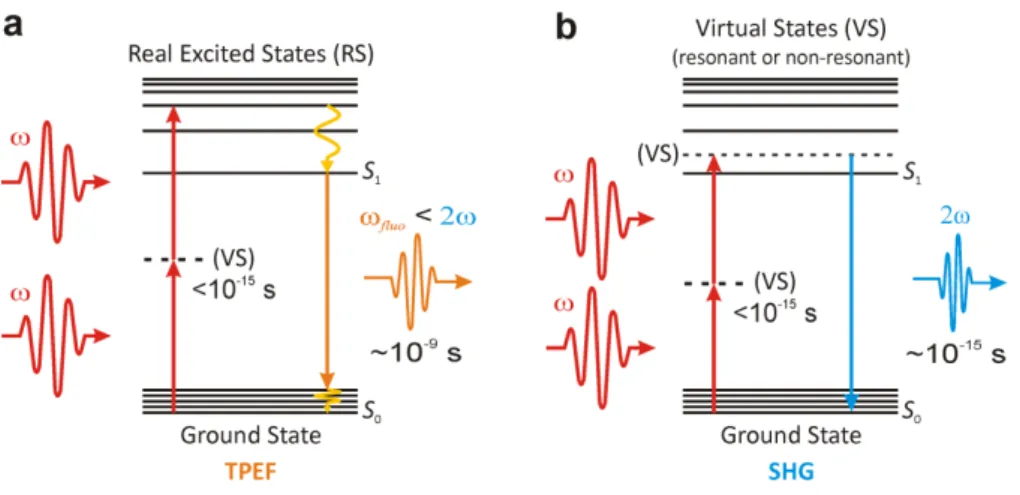
Chapter III | Coherent second-harmonic microscopy for detection of single semiconducting QDs ... 35
III.1 Contrast mechanisms for two-photon nonlinear microscopy ... 36
III.1.1 Two-photon excited fluorescence ... 36
III.1.2 Second-harmonic generation ... 38
III.2 Second-order nonlinearity of CdTe – from bulk to single QD scale... 41
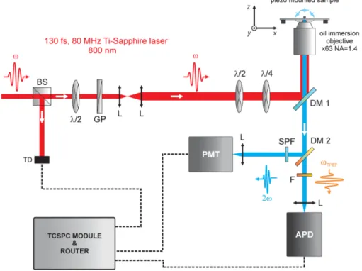
III.3 Nonlinear two-photon polarization sensitive microscopy setup ... 45
2 | Contents
III.4 Time correlated single photon counting in detection of single nanoparticles ... 51
III.5 Chapter summary ... 53
Chapter IV | Second-harmonic generation from CdTe QDs: single dot studies ... 55
IV.1 SHG from single dot-shaped CdTe/CdS core/shell QDs ... 56
IV.1.1 Spectral dependence of the SHG process from spherical CdTe/CdS core/shell QDs ... 59
IV.1.2 Contribution of the CdS shell to the overall SHG emission process ... 62
IV.1.3 Orientation dependent SHG polarization response from spherical CdTe/CdS core/shell QDs ... 63
IV.1.3.1 Analysis of the SHG polarization dependence ... 64
IV.1.3.2 SHG polarization response with respect to the CdTe symmetry constraint ... 68
IV.2 SHG from single rod-on-dot CdTe/CdS heterostructures ... 70
IV.2.1 Special features of SHG emission from rod-on-dot QD heterostructures ... 73
IV.2.2 Polarization analysis of the SHG emission of rod-on-dot CdTe/CdS QDs ... 78
IV.2.2.1 Simulation model for polarization analysis of RD QD heterostructures ... 80
IV.2.2.2 The role and impact of the CdS rod length into the total SHG intensity... 81
IV.2.2.3 Errors in inferring the orientation of the crystalline lattice from SHG polarization analysis ... 85
IV.3 Accuracy of the polarization analysis from a reduced set of raw data points ... 86
IV.4 Chapter summary ... 89
Chapter V | Size dependence of the second-order nonlinearity – single dot and HRS studies ... 91
V.1 Size dependence of SHG from single CdTe quantum dots ... 92
V.1.1 Detection threshold of the size dependent SHG signal intensity ... 93
V.1.2 Estimate of the second-order nonlinear susceptibility ... 97
V.1.3 Error sources in determining the size dependence of the second-order nonlinear susceptibility ... 99
V.2 Hyper-Rayleigh Scattering from CdTe QDs ... 101
V.3 Relations between spectral and size dependence of CdTe χ(2)features ... 105
V.4 Chapter summary ... 107
General conclusions ... 109
Appendix A: Correction of the raw data for SHG wavelength dependence ... 113
Appendix B: Model for SHG polarization response of spherical CdTe/CdS QDs ... 121
Appendix C: Model for SHG polarization response of RD QD heterostructures ... 133
Appendix D: The list of publications ... 145
Introduction
Recent achievements in fabrication and characterization of inorganic nanoparticles of high optical quality have inspired new areas of research into the fundamental properties and applications of these nanoscale materials. Basically divided into metals, semiconductors and insulators, morphologically and geometrically tailored nanoscale systems are driven in order to selectively combine desirable properties at the sub-wavelength regime towards optical probing. This approach becomes particularly fascinating and challenging when is put on nonlinear optical effects occurring with small nanoparticle assemblies of typical size below 20 nm. At this scale, the electronic properties of such small nanostructures lie at an intermediate distance between those of a single atom and those of bulk materials. In consequence, this scale provides an inspiring avenue onto the molecular regime for physical properties better known at the bulk level, possibly leading to novel and remarkable responses, depending on size, composition and shape of the nanocrystals.
Applied nanoscale nonlinear optics has reached a certain limit in size dependent detection efficiency of weak signals in nonlinear processes, e.g. in our case the lowest-order nonlinear scattering which is known as second-harmonic generation (SHG). Recent efforts in detection of nonlinear scattering from noncentrosymmetric nanocrystals, deriving from the high nonlinearities of their well known bulk counterparts such as KTiOPO4 (Le Xuan et al. [1]) or BaTiO3 (Hsieh et al. [2]), have shown photostable and efficient SHG emission with a high damage threshold for these nanoparticles. None of these efforts, however, has been able to pass a ~40 nm size barrier, thus remaining at the level of large nanoscatterers while resorting to the most sensitive available technologies for SHG detection. As we realize now, this barrier can be overcome when replacing dielectric insulators by direct-gap semiconducting materials.
4 | Introduction
Shrinking the size while maintaining an efficient coherent scattering process requires a new approach towards nanoengineering of semiconducting nanoscale heterostructures as potential sources of enhanced optical nonlinearities. This approach has been introduced nearly a decade ago by Jacobsohn and Banin [3] and demonstrated at a preliminary level by hyper-Rayleigh scattering (HRS) from a colloidal suspension of II-VI semiconductor CdSe quantum dots (QDs), with sizes varying from 20 to 100 Å. A strongly size dependent, incoherent SHG signal was evidenced and attributed both to the nanocrystal volume and its surface. Nevertheless, the crucial experimental evidence that 10 to 15 nm large QDs can emit the coherent SHG at a detectable level in the case of single nanoparticle studies remained elusive. Therefore, this was the prime objective of this work.
Indeed, for the first time, we have successfully surpassed this single nanoparticle size barrier by considering two-photon resonant SHG in individual QDs, in order to find an alternative emission system for fluorescent nanolabels. In our first work (Zielinski et al. [4]), we shown that highly nonlinear zinc-blende structures like CdTe QDs are ideally suited for this task. Due to their perfectly octupolar crystalline structure, size scaled energy band gap, and above all, high values of nonlinear coefficients, CdTe nanocrystals of about 12.5 nm diameter can efficiently provide very high SHG count rates, as high as 105 Hz. Additionally, remarkable sensitivity to orientation of the crystalline lattice was clearly demonstrated. Moreover, quantum confinement effects have been found to strongly contribute to the second-order nonlinear optical susceptibility, suggesting that QD scale materials are not limited by their bulk properties. Hence our attention focused on quantitative characterization of the nonlinear susceptibility of quantum confined QDs by way of their spectral dispersion and size dependence. Using single particle spectroscopy and ensemble HRS methods, we shown that under appropriate conditions, the nonlinear susceptibility of quantum confined structures can significantly exceed that of bulk (Winter et al. [5]), and therefore allow for better understanding and control the nonlinear properties at the individual QD scale.
Further motivations of this work originate from the interest in the engineering of high optical nonlinearities, by the optimal choice of semiconducting materials with adequate electronic properties. Our ambition is to extend their range to any particular application in high resolution microscopy. Current studies carried out by several research groups, designate many possible ways towards such goal, each of them involving electronic band structure engineering, and excitonic or electron–plasmon interactions of hybrid heterostructures of high complexity. Worth mentioning here is, the work presented by group of Psaltis [6], on huge
Shrinking dimensionality of the bulk into the quantum dot scale | 5 Introduction |
SHG nanocavity-like enhancement in ~80 nm large BaTiO3 nanoparticles covered by a ~10 nm thick gold shell. In addition, interesting approach of synergistic SHG coupling of gold nanorods into a semiconductor QD cores (Shaviv and Banin [7]) are worth attention. At a more basic level, a novel approach for SHG obtained from purely semiconducting materials can attract a significant interest. As a proof-of-principle experiment, composite rod-on-dot hybrids built from different crystalline symmetry moieties were recently reported (Zielinski et al. [8]), as capable to further improve initially reported results. Their high quadratic nonlinearity was precisely engineered following the blueprint of a pointwise sum of the susceptibilities for each of the components. The nonlinear susceptibility of such hybrid leads to a significant SHG enhancement assigned to slower decoherence and improved spatial charge separation upon excitation, which exceeds that of ‘mono-compound’ material QDs.
This thesis is organized as follows: Chapter I provides an introduction to the downscaling of semiconductors from bulk to the nanoscale. Quantum confinement effects in nanoparticles of different dimensionality are explained using a simple ‘spherical box’ approximation. These fundamental properties are further investigated towards a better understanding of the electronic band structure as well as optical interactions in QDs. Chapter II deals with fabrication and characterization of suitable materials for second-order nonlinear microscopy, this imaging method being then reviewed in Chapter III. Coherent SHG emission from isolated mono-compound CdTe QDs and hybrid rod-on-dot semiconductor heterostructures is investigated in Chapter IV. These studies focus on spectral features of the second-order nonlinear optical susceptibility of both types of materials. Strong orientational dependence of the SHG tensorial features is pointed out, allowing to infer the spatial orientation of each single nanocrystal. Chapter V addresses single nanoparticle spectroscopy and HRS studies of the size dependent nonlinear susceptibility of CdTe QDs. These studies, together with spectral features reported in the preceding chapter, demonstrate the superiority of QDs over the bulk in the context of second-order nonlinear properties. In the last part of the thesis we provide details about the simulation algorithms used in this work. Finally, this work is summarized and final conclusions and future prospects are drawn.
7
Chapter I
|
Optical properties of semiconducting quantum confined
heterostructures
I.1 Shrinking dimensionality of the bulk into the quantum dot scale ... 8
I.1.1 Quantum Confinement ... 8
I.1.1.1 Density of states ... 12
I.1.1.2 Coulomb interactions and confinement regimes ... 14
I.1.2 Band structure of CdTe ... 16
I.2 Optical interactions ... 17
I.2.1 Scattering ... 19
I.3 Chapter summary ... 20
The case of nanoscale semiconductors illustrates the understanding of material properties as a function of size and composition. In this chapter the key features of quantum confined semiconducting structures are briefly introduced, following the literature. Our interest here is to point out the originality of semiconducting nanocrystals (SC NCs) in the context of their optical features. Firstly, we start by explaining the quantum confinement effect, using a simple model, and show how SC properties evolve while crystal dimensionality decreases, starting from the bulk all the way to a single quantum dot. We point out how the NC shape and its material composition translate onto the optical properties, and explain optical excitation mechanisms in relation with absorption and scattering processes. Finally the electronic band structure of bulk CdTe is discussed and compared to that of a single CdTe QDs.
8 | Optical properties of semiconducting quantum confined heterostructures
I.1 Shrinking dimensionality of the bulk into the quantum dot scale
The properties of quantum confined SC NCs place these materials between isolated atoms (or small molecules) and a bulk phase of condensed matter.9 Like in any material, fundamental electrical and optical features of SCs vary when the size is reduced and the electronic energy level spacing exceeds different energies characterizing the structural properties, e.g. the temperature of the surrounding environment (kT), the binding energy or the exciton Rydberg energy. Here we show that this size dependence becomes extremely significant when the crystal is shrunk into a quantum confined structure. Semiconductor crystals, where the Fermi level lies between two bands (Figure I-1) exhibit completely different behavior from that of metals or insulators. The band edges dominate the low-energy optical and electrical interactions, so optical excitations across the band gap (BG) depend strongly on cluster size variations (for clusters starting from approximately 10,000 of atoms). This leads also to strong size dependence of electrical carriage transport through the crystalline volume due to the energy variations required for charge appearance or withdrawal on the NC.10
Figure I-1 | Comparison of the changes in the electronic structure accompanying a reduction in size, in metals
and semiconductors.
I.1.1 Quantum Confinement
The first attempts in understanding the quantum mechanics of confined SC NCs were considered nearly three decades ago, resulting in a description of diffraction by the charges (electrons and holes) of the periodic lattice potential in the semiconductor NC.11-13 A key feature of SC materials is that charge diffraction leads to a characteristic band structure,
Shrinking dimensionality of the bulk into the quantum dot scale | 9
Figure I-2 | Comparison of the energy levels of conduction and valence bands as well as band gaps for different
bulk semiconducting materials (II-VI groups SC compounds).14-15
where allowed electronic energy states exhibit the form of broad valence and conduction bands (VB and CB, respectively), resulting from a complex set of anisotropic relations between energy and momentum.14 At the macroscopic scale, the bands are continuous, and the energy band gap (EBG) between them is a fixed parameter, determined by the crystalline material composition (Figure I-2). However, decrease in dimensionality of the SC heterostructure, where at least one of the dimensions (Lx(y,z), see Figure I-3) is under quantum
confinement regime results in more confined electronic excitations due to the interaction between the nanoparticle (NP) boundaries (with energies between the orbital spacing) and confined electrons. Decrease in the NC size also increases the energy band gap, as confirmed by the blue-shifted luminescence. In direct-gap size confined SC NCs (such as II-VI SCs), absorption of a photon above the BG usually leads to generation of a single, Coulomb attracted electron-hole pair (an exciton, confined by the material boundaries) and its quick relaxation, with simultaneous reemission of a new photon, which has an energy exactly matching the BG. For example, in CdSe QDs the shift of energy gap varies from 1.2 eV up to 3.0 eV (while its bulk BG energy is equal 1.71 eV).16
This effect, however, can be controlled also by composition of the material, e.g. different size of the CdSe and CdTe QDs span the visible (VIS) spectral region,17-21 whereas PbS QDs traverse from VIS to the near infrared (NIR),22 while materials like ZnSe exhibit efficient luminescence in the ultraviolet (UV).23
10 | Optical properties of semiconducting quantum confined heterostructures
In the first approximation, quantum confinement can be described using a simple ‘spherical box’ model,11-12,24 where the SC NC is embedded inside an insulating matrix, as illustrated in Figure I-3(d). The exciton resides in the infinite potential well, which leads to a quantized valence and conduction band structures exhibiting ladder-like discrete energy levels for both hole and electron.
In other words, for an ideal SC NC, quantum confinement occurs when the width of the infinite potential approaches the exciton Bohr radius of the material aB =h2ε/m er 2, where
r
m stands for the reduced mass of the exciton, and
ε
for the dielectric constant of the material. When the width of the infinite potential well is comparable to a (exactly like in the B case of QDs), the VB and CB split into discrete energy surfaces in k-space. In such a case, the Schrödinger equation take the following form:25( )
( ) ( )
( )
2 , , 1 , , , 2 me h( )z ψn U ψn En kψn −ℏ ∇ ∇ k r + ɶ r k r = k r (I.1)where the infinite potential Uɶ
( )
r =V( ) ( )
r +U z and the effective masses of the hole and electron me h, ( )z depend on the coordinate z of the confined direction due to the bandgap mismatch. We assume Bloch function – like eigenstates subsequently summed over k to describe bonding between the delocalized molecular orbitals (MOs), to be identical throughout the various material shells:( )
( )
, ,
ik r
k u k u
u r =e ⋅ χ r (I.2)
where χk u, is subject to the periodicity of the unit cell (with relatively weak k dependence), the eik r⋅ factor is a plane wave-like factor with a wavelength
λ
=2 / kπ
longer than that of the unit cell. The Bloch MO in the case of a single k is infinitely delocalized.Following this assumption, the wave function takes the form:
ψ
( ) ( ) ( )
k r, =u k r,φ
z , where( )
zφ
is the ‘envelope function’ of the confined state. Combining the Bloch function behavior with the Schrödinger equation, we obtain:( )
( ) ( )
( )
2 ,0 , 1 2 e h( ) n z U z z E z m z φ φ φ −ℏ ∇ ∇ + = (I.3)Shrinking dimensionality of the bulk into the quantum dot scale | 11
For infinitely high barriers of the potential barrier, the energy of the n-th state confined in a rectangular potential well (2D) of width Lz is:
( )
2 2 2 ,0 2 , 2 2 n e h z E n D m L π = ℏ (I.4)Further reduction of the SC NC dimensionality (illustrated in Figure I-3) by confining in Lx
and Ly directions lead to quantum rods (QRs) and QDs. Therefore the quantum energies of the
n-th confined states inside the infinite potential barrier can be expressed as:
( )
2 2 2 2 , 2 2 , 1 2 y z y z n n e h y z n n E D m L L π = + ℏ (I.5)( )
2 2 2 2 2 , , 2 2 2 , 0 2 x y z y x z n n n e h x y z n n n E D m L L L π = + + ℏ (I.6)These expressions lead to a simple common conclusion: the energy of an extra electron in a tiny semiconducting crystallite structure amounts to the conduction band energy (Ec) plus the quantum localization energy of a ‘pseudo electron’ of effective mass m (treated as a pseudo e particle), which has no direct relationship with the real electron mass, and often displays a smaller value.12
The wave function
ψ
n( )
k r, , as a product of an ‘envelope function’ and a Bloch function can be generalized to determine confined VB and CB states in the wake of progressive reduction of the dimensionality (where coupling between the bands has to be considered). Generalized forms for the CB wave function( )
s
e m
ψ
r and VB wave functionψ
h( )
r can be written as follows:25( )
( ) ( )
1 , 2 s s e e e m z um x y ms ψ r =φ = ± (I.7)( )
( ) ( )
3 1 , , 2 2 j j j h h h m m j m z u x y mψ
r =∑
φ
= ± ± (I.8)12 | Optical properties of semiconducting quantum confined heterostructures
I.1.1.1 Density of states
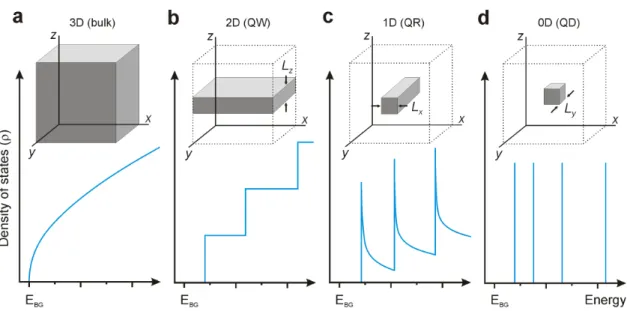
As illustrated in Figure I-3 the density of states
ρ
(DOS) critically depends on the NC dimensionality. The DOS expresses directly the number of possible solutions of the Schrödinger equation (I.1) within a given interval eigenstate energy E and is seen to depend on the structure confinement:( )
2 3 2 3 m mE D ρ =π ℏ (I.9)(
)
( )
2 z 2 z n n z m E E D Lρ
θ
π
= ℏ∑
− (I.10)( )
, , 2 1 1 z z y z n n y z n n m D L L E Eρ
π
= −∑
ℏ (I.11)(
, ,)
( )
, , 2 0 z z z z z z n n n n n n x y z E E D L L Lρ
=∑
δ
− (I.12)A detailed discussion how the SC NC shape impacts on the optical properties can be found for example in an excellent review by Scholes.26 Here we explain only how the shape influences the major DOS features, which are directly related to the SC NC optical properties. In our considerations the most important features are that of QRs and QDs. In the case of the QRs, the DOS is strongly peaked and decays as 1/ E (Figure I-3(c)). Heavy and light hole
sub-bands are mixed, leading to coupling between the energy levels of the VB.27
On the contrary, QDs exhibit atypical Dirac
δ
( )
E function like behavior for 3D confined DOS, which allows for accommodation of only two carriers of opposite spins on a single quantized energy level, therefore called “artificial atoms”. The first approximation model of the parabolic band, however, does not fully reflect the real complexity of the QD DOS, because there are no SCs exhibiting such simple parabolic conduction and valence bands.11 Therefore, more realistic approaches have to be considered, e.g. the multiband effective mass approximation,16,28 which takes into account degenerated sub-bands, dispersion of light and heavy hole branches for non-zero k, and spin-orbit splitting of the electron sub-bands. The multiband effective mass approximation is more efficient in quantitative description of theShrinking dimensionality of the bulk into the quantum dot scale | 13
optical properties of SC NCs than the parabolic approximation, and can be used in order to describe the transitions between the quantum size levels (QSLs), and to calculate their energies.16,28
Figure I-3 | Schematic representation of decreasing dimensionality of a SC crystal from bulk (a), quantum well
(QW, (b)), and quantum rod (QR, (c)) into the single QD scale (d), as shown with corresponding densities of states (ρ).
For tight-bounded semiconducting NCs, the frequency dependent rate of a spontaneous transition from an excited electron-hole state j to the ground state 0 can be determined from Fermi’s ‘golden rule’ namely:29
2 2 2 3 0 3 j j e o j m c
ω
πε
Γ = p ℏ (I.13)where e is the electron charge, ε0 is the permittivity of vacuum, m is the electron rest mass,
j
ω is the frequency of the emitted light, and o p j is the matrix element of the momentum, related to the dipolar matrix element by o p j =i mωj o r j .30 Note, that this dependency applies to both absorption, and scattering processes. The size dependence of
j
Γ is determined by that of the matrix element modulus o p j and the emission frequency
j
14 | Optical properties of semiconducting quantum confined heterostructures
expressed as a product of the Bloch function u r
( )
and an ‘envelope function’φ
( )
r , and the matrix element of the momentum for an allowed transition is given by uCB p uVB .29-30 Therefore the interband transitions are largely determined by crystalline lattice defined Bloch functions, and the uCB p uVB term does not depend on the NC size. The decay rate of an ideal two-level exciton is expected to be proportional to the emission frequency, e.g.j const ωj
Γ = ⋅ .31
I.1.1.2 Coulomb interactions and confinement regimes
In strongly confined structures, positions of the electrons and holes are constrained. Electrostatic screening is less effective, leading to reduction of the effective dielectric constant
ε
, which results in an increase of the binding energy (E ). For strong enough B confinement, Coulomb interactions can be neglected in the confinement direction. In such conditions the single particle ‘envelope function’ ,( )
,
e h e h
z
φ can be used in order to describe the exciton wave function:
(
,)
e( ) ( ) (
h ,)
X
φ
zeφ
zhφ
Φ r re h = ̻ ̻e h (I.14)
where the
φ
(
̻ ̻e, h)
function accounts for the in-plane confined motion of the electron andhole expressed with respect to respect to in-plane coordinates ̻e,h. The in-plane wave function
φ
(
̻ ̻e, h)
abides to a single-particle Schrödinger equation (with an effectiveexcitonic potential U ):X 25
(
)
(
)
(
)
(
)
2 2 , , , 2 me mh φ UXφ EBφ − ∇ + = + ℏ ̻e ̻h ̻e ̻h ̻e ̻h (I.15)where: me+mh =Mexciton is the exciton translation mass. The remaining dispersion of the exciton is expressed by its kinetic energy: Ekin =ℏ2K2 / 2Mexciton (with K as the excitation vector). A similar rules holds for the QRs, therefore their shape has no impact on the binding
Shrinking dimensionality of the bulk into the quantum dot scale | 15
energy. For both, 1D and 0D confined structures it is only the strength of the confinement which determines E . B
The strength of the quantum confinement is related to the Coulomb energy of the electron-hole interaction, which is of the order of e2 /εa. As the size is downscaled, the quantization energy increases as 1 / a2, therefore the Coulomb energy, which scales as 1/ a becomes only a small correction factor.16,21 On the contrary, for larger SC NCs the Coulomb electron-hole interaction may surpass the quantization energy. These interactions define the quantum confinement regime, which can be characterized by the ratio between the NC radius, a, and the Bohr radius a of the bulk exciton. From there on, three different quantum confinement B regimes can be distinguished:24,32
‘Weak confinement regime’, where a≫aB, and the binding energy of an exciton, Eexc, is larger than the quantization energy of the electrons and holes. In first approximation, the exciton ground state energy is then expressed as:32
2 2 2 2( ) BG exc e h h h E E m m a
π
ω
= − + + (I.16)Under a weak confinement regime, Coulomb interactions between the electron and hole are strong and have to be taken into account.
‘Intermediate confinement regime’, which occurs in the SCs exhibiting different effective masses of the electron and hole in an intermediate size ratios ae > >a ah, where
2 2
( ) / ( )
e h e h
a =h
ε
m e are the Bohr radii of electron and hole, respectively. In this regime, the hole moves in the average potential of a much faster electron (about three orders of magnitude), and stays localized in the center of the NC. The region of its motion around the NC center is much smaller than a, therefore size dependence of the exciton ground state may be determined as a localized donor.‘Strong confinement regime’ occurring for small NCs, where a≪aB. The electron-hole Coulomb interactions are surpassed by the quantization energy of transitions, so the reduction of the transition energies is relatively small. Interband transitions between quantum-size energy levels of the parabolic VB and CB are governed by selection rules, which limit allowed transitions to levels with the same quantum numbers.
16 | Optical properties of semiconducting quantum confined heterostructures
I.1.2 Band structure of CdTe
The band structures of typical II-VI group bulk semiconductors have been well researched using, e.g. ‘semi-ab initio‘ approach.33 Figure I-4(a) illustrates band structures for the case of bulk zinc-blende CdTe crystal, where a single Brillouin zone stems from the Bloch wave of the face-centered cubic crystalline periodic structure of the CdTe crystal. The wave vector k
crosses the critical points of the crystalline symmetry, which are as follows: L – a center of a hexagonal facet, Γ– center of the Brillouin zone, X – center of a square facet, and K – middle of an edge joining two hexagonal facets. The center point Γ determines the band edges for the parabolic VB and CB in the first approximation model.
Early efforts on measurements and assignments of the size dependent optical spectrum in QDs were constrained by difficulties in preparation of weakly dispersed, high quality colloidal QDs, with well maintained control over the size dispersion. Successful assignment of the lowest quantized energy levels in many SC QDs could be obtained from a single-band effective mass model.34 Assignment of the higher excited quantized levels remained difficult due to, e.g. valence-band degeneracy in zinc-blende CdTe QDs,35 where the conduction band is made of s orbitals of cadmium and its valence band is composed of p orbitals of tellurium. Following the work of Masumoto et al. [36], the orbital angular momentum in CdTe QDs is mixed with spin angular momentum, and the valence band is split into the topmost J =3 2
band and the split-off J =1 2 band. Quantum confined hole envelope function has an additional angular momentum L, therefore possible L – J coupling may lead to a complicated energy level structure for the VB. Nevertheless, CdTe has a less complicated VB than wurtzite CdS and CdSe QDs, and exhibits a larger spin orbit splitting of 0.927 eV and a smaller EBG= 1.44 eV, therefore the split-off band is expected to mix weakly with the topmost VB.
Since advances in colloidal synthesis techniques allows to obtain NCs of a sufficient quality, e.g. CdSe and CdTe QDs, assignments of multiple numbers of states using size-dependent photoluminescence excitation (PLE) spectroscopy at cryogenic temperatures close to 0 K were carried out with some success.18,36
Optical interactions | 17
Figure I-4 | a) The band structure of the bulk, zinc-blende like CdTe crystal. Critical points of the Brillouin zone
are explained in the text. Adapted from Huang et al.33 b) Spacing of the excited states of strongly confined CdTe QDs. Dashed lines (labels from b to f) correspond to the transitions 2SDD3 / 2→1Se, 1PFP3/ 2 →1Pe,
5 / 2
1PFF →1Pe, 2PP1/ 2 →1Pe, 2PFF5 / 2 →1Pe, and (label b’) 3SDD3 / 2 →1Se, calculated using the data from Ref. [35], assuming that the lowest burned structure correspond to the transition 1SDD3 / 2 →1Se. Straight lines (from 1 to 5) represent experimentally measured data, with the converging point at the lowest exciton energy transition of bulk CdTe, at 1.596 eV. Figure adapted from Ref. [36].
Spacing between the excited states of several samples of strongly confined CdTe QDs is illustrated in Figure I-4(b). The quantized energies of 1SDD3/ 2 and 1PFP3/ 2 states vary by about 0.1 eV, however the energy separation between these states changes at most by 6.4 meV. On the other hand, the energy separation 1SDD3/ 2 and 1PFP3/ 2 for ~2 nm large dots changes significantly by 68 meV, due to a strongly varying effective mass of the electron. The absorption spectrum of ~5.1 nm large dots exhibits an energy splitting of about 44 meV, showing strong dependence on the QD sizes, however there was no experimental effort towards large-size CdTe QDs, which reach the region close to the intermediate confinement regime of about 10-12 nm diameter.
I.2 Optical interactions
Both linear and nonlinear optical properties in SC QDs result from the transitions between the electron and hole QSLs. In linear process, as recalled, the absorption of an electron from the VB into the CB can be triggered by the absorption of a photon with energy above the BG. In
18 | Optical properties of semiconducting quantum confined heterostructures
general, direct semiconductors transitions involve electrons and holes of equal momentum, for which the spectral distribution of possible transitions is described by the optical DOS:37
( )
2(
( )
( )
)
,
DOS e h
e h
O ℏ
ω
=∑∫
Mδ
E k −E k −ℏω
dk (I.17)The Dirac
δ
function ensures energy conservation, with summation over a system dimensionality dependentk
vector. The optical matrix element can be calculated for a dipole approximation from the wave functions (I.7) - (I.8), and takes the following form:( ) ( )
s s j s j e h e h e h m m m m m M =ψ
ε⋅pψ
=∑
φ
rφ
r ⋅ u ε⋅pu (I.18)The oscillator strength is directly proportional to the overlap of the ‘envelope functions’ of the recombining excitons, which prevents transitions between levels of opposite parity. The second term on the right-hand side of the expression determines the product of the polarization vector ε and the momentum operator
p
between the Bloch functions (known asthe Kane matrix element). It imposes additional selection rules on the polarization of the absorbed/emitted photon in interband transitions, which is determined by the heavy or light character of the hole.
For the first approximation, the absorption spectra (electron-hole interactions) under strong quantum confinement is given by:11-12,16
( )
( )
1.8 2 2 2 2 1.8 2 2( ) h e BG BG e h e e E E a E a E a m m a a ν ν ν ν νπ
ω
ε
ε
= + + − = + − + ℏ ℏ (I.19)where Eνh e,
( )
a ∼1/a2 are the energies of theν
th hole and electron QSLs, respectively. TheCoulomb interaction can be calculated from first order perturbation theory. Recombination of the exciton may be assisted by the emission of the photon, which possesses an energy
/
hc
ω
=λ
ℏ and a momentum kν =2 /π λ (negligible when compared to that of the exciton), where
λ
the photon wavelength and c the speed of light. The energy of the lowest transition for a known Bohr radius a , and effective masses of the electron and hole B me h( ), for a parabolic band inside an infinite potential (ψ ψe = h) is given by:2 B a E a π ∆ = R (I.20)
Optical interactions | 19
where: R=h2 / 2m ar B2 is the exciton Rydberg energy, dependent on the reduced mass of the exciton.
Radiative relaxation of the exciton exhibits nearly single-exponential character of the emission decay curves. At a given size dependent emission frequency, all the QDs are therefore expected to emit the light at the same rate. The emission decay rates increase with the frequency. Considering the complex structure of CdTe VB, where several hole levels are located close to the band edge, leads to exciton states lying close to the lowest excitation energies. These excitons exhibit much lower probability for spontaneous decay to the ground state, and a high rate of exchange with the lowest energy exciton. The population of the lowest energy exciton is then reduced due to thermal distribution, leading to a lowered rate of the radiative recombination and increased rate for dark excitons.20,29
I.2.1 Scattering
Non-resonant excitation, where the energy of exciting photon does not match k = 0 transitions, can leads to generation of an exciton, with an excess kinetic energy:
2 2 , 2 kin e h k E m ∆ = ℏ (I.21)
Before it recombines such an exciton loses all or part of this kinetic energy, then relaxes towards the band edge. Relaxation of a non-resonant exciton leads to inelastic scattering, where the kinetic energy is not conserved. In zinc-blende CdTe nanocrystals excess energy of the exciton is carried out by longitudinal optical phonons (LO).38 The energy level structure of CdTe is such that the electrons are completely delocalized in the CB, and holes are localized in the VB, where the level spacing is very small, because an effective mass of the hole is much larger than the effective mass of the electron (mh ≫me), the relaxation of the hole leads to its coupling with 1 LO phonon. Decreasing of the energy level spacings in the CB may lead to coupling of the electron with several LO phonons, and decrease for higher energy levels down to 1 – 2 LO phonons.
20 | Optical properties of semiconducting quantum confined heterostructures
I.3 Chapter summary
In conclusion, this chapter contains a theoretical introduction to physical properties of semiconductor NPs, and explains how these properties evolve with the decrease of their size, and how they impact on to the optical features of the nanoscale structures. Quantum confinement effects related to the size, material composition, as well as to the shape of SC NC have been discussed. We point out how Coulomb interactions and the binding energy of the QD structure change with increasing quantum confinement, and explained how these interactions are breaking down into different quantum confinement regimes. Understanding these properties allowed for the introduction of the band structure of the CdTe crystal, where the bulk structure has been compared with that of a single CdTe QD. Finally we have described fundamental optical interactions, which occur in QD structures, showing that both linear and nonlinear optical properties of SC crystals result from transitions between the electron and hole quantized energy levels.
21
Chapter II
|
Colloidal CdTe-based QD samples: synthesis and
characterization
II.1 Guidelines for material selections ... 22 II.2 Characterization of dot-shaped CdTe/CdS core/shell QDs ... 22 II.2.1 Chemical synthesis of dot-shaped CdTe/CdS core/shell QDs ... 23 II.2.2 Shape and size distribution of dot-shaped CdTe/CdS QDs ... 23 II.3 Synthesis and characterization of dot-shaped CdTe QDs ... 25 II.4 Characterization of rod-on-dot CdTe/CdS heterostructures ... 27 II.4.1 Chemical synthesis of rod-on-dot CdTe/CdS heterostructures ... 29 II.4.2 Shape determination and effective size distribution of RD CdTe/CdS heterostructures .... 30 II.5 The role and importance of the shell in type-II QDs ... 32 II.6 Sample preparation ... 33 II.7 Chapter summary ... 34
Over the last decade, significant advances in the field of NP synthesis enabled fabrication of increasingly complex heterostructures. Composite materials that simultaneously retain quantum confinement are therefore becoming of interest towards the nonlinear optics, mainly due to the enhancement of their nonlinearity. This lead us to propose SHG active CdTe based semiconducting QDs and QD heterostructures as promising candidates for nanolabels in nonlinear microscopy. The following chapter contains structural characterization of dot-shaped QDs and rod-on-dot QD hybrids, which have been used throughout this work. We describe their morphology, methods for their synthesis, and give details about sample preparation for microscopic measurements at the sub-wavelength single QD scale.
22 | Colloidal CdTe-based QD samples: synthesis and characterization
II.1 Guidelines for material selections
The contents of this work deal mainly with an investigation of the second-order nonlinear optical properties of NPs exhibiting enhanced nonlinearity, thus opening the way towards decrease of their size and application to two-photon scanning microscopy (TPSM). These NPs have been obtained from semiconductors rather than from insulating inorganic materials, to as to be in a position to benefit from quantum confinement effects. We have chosen to work mainly with CdTe QDs and CdTe/CdS quasi-type-II QDs for the reasons outlined hereafter. Firstly, CdTe exhibits a relatively strong second-order nonlinearity from a noncentrosymmetric zinc-blende – like crystalline lattice structure.4-5 The energy band gap of CdTe is 1.44 eV,14-15 and it can be tuned up to approximately 2.0 eV as a function of QD size. This appears to match the correct range of available frequencies from a Ti-Sapphire femtosecond oscillator. CdTe has the refractive index of about 3.0 at ~1.5eV (295 K), and it is nearly transparent for NIR range.39 Another important issue is the following: in a strong quantum confinement regime (when QD sizes are about that of the exciton Bohr radius aB or smaller), the transition dipole moment of these NPs or their two-photon cross-section does not follow the same scaling rules as observed for the bulk, but evidence significant enhancement.5 This makes SC colloidal QDs promising candidatess for nonlinear optical microscopy.
II.2 Characterization of dot-shaped CdTe/CdS core/shell QDs
Over the last decades, significant advances in the field of semiconductor nanoparticles synthesis enabled fabrication of various core/shell heterostructures.40-42 During this period well developed methodologies of colloidal quantum dot synthesis were defined and implemented, resulting in a high reproducibility and good optical quality of the NPs, to a level making them compatible with commercial exploitation.
In dot-shaped quasi-type-II CdTe/CdS NCs, CdTe has a zinc-blende structure (with 43m point group symmetry). A stereograph showing the symmetry elements of 43m group is presented in Figure II-1(a). It consists of three 4-fold inversion axes perpendicular to four {1,1,1} cube facets, four 3-fold axes along the main diagonals, and six planes of symmetry along the diagonals of facets. Additionally, a set of 24 equivalent points is presented.14,43-44 The single crystalline unit cell of a CdTe zinc-blende like structure is shown in Figure II-1(b).
Characterization of dot-shaped CdTe/CdS core/shell QDs | 23
II.2.1 Chemical synthesis of dot-shaped CdTe/CdS core/shell QDs
Synthesis of the CdTe/CdS core/shell NPs dedicated to SHG emission required NC sizes of about 10–15 nm diameter. CdTe/CdS dot-shaped QDs used in this work were prepared in a non-coordinating solvent, following the main lines of the procedure given by Peng and coworkers.45 A scheme of the synthesis and apparatus is shown in Figure II-2(a,b). The synthesis was carried out under argon atmosphere. In short, 0.1 mM CdO was dissolved in 5 ml of octadecene (ODE) and 0.06 g tetradecyl phosphonic acid and heated-up to 280 °C. At this temperature 0.1 mM Te dissolved in trioctylphosphine (TOP) is injected, leading to the formation of approximately 4 nm diameter quantum dots. These were further grown at 290 °C by additional multiple injections of a 0.1 M cadmium oleate solution in ODE and 0.1 M TOP:Te until the emission peak reached about 760 nm (Figure II-3(c)). Once the cores have reached the desired size, the temperature was decreased in order to thermodynamically terminate their growth. The solution was heated again when TOP:Te injections were replaced by TOP:S to initiate shell growth. Injections of sulfur containing reagent were sufficient to form approximately three monolayers of CdS shell, resulting in the formation of an approximately 1 nm thick CdS layer (Figure II-3(b)). Particles were then dissolved in toluene and precipitated by addition of methanol and centrifugation.
II.2.2 Shape and size distribution of dot-shaped CdTe/CdS QDs
Transmission electron microscopy (TEM) characterization shown that particles are somewhat ellipsoidal, with an effective diameter of 10.9 ±1.8 nm (considering the square root of the product of the short and long axes), and a typical ellipticity of 1.17 ±0.13. A typical TEM image (obtained with a Philips CM120 Super Twin transmission microscope) of several NPs appears in Figure III-3(a). Under the prescribed synthesis conditions, some ripening occurs during CdTe NC growth, leading to some relative broadening of the size distribution. The largest particle observed using TEM had an overall (core + shell) effective diameter of 15 nm, while the smallest observed particles had an effective diameter of about 10 nm.
Alternatively, the size distribution was confirmed using calibrating curves proposed by the group of Peng et al.,45 where the emission peak position determines the quantum dots size (neglecting the relatively small Stokes shift of about 8 nm between the emission and first
24 | Colloidal CdTe-based QD samples: synthesis and characterization
excitonic absorption peaks at these sizes), following the empirical function for CdTe QDs given below:
(
9.8127 10 1.7147 10 1.0064 194.84D= ⋅ − ⋅ + −
where D (nm) is the NC diameter, and
absorption peak of the corresponding sample. The sizing curve obtained with thi function is shown in Figure
II-Figure II-1 | a) Stereograph presenting the symmetry elements of
unit cell. The lattice constant is a0 = 0.6482 nm.
Figure II-2 | a) Synthesis way of CdTe/CdS dot
synthesis apparatus (Ar – argon flow; TC
of diluted QDs colloidal solution, carried out in order to control the NPs size
based QD samples: synthesis and characterization
peaks at these sizes), following the empirical function for CdTe QDs
)
(
)
7 3 3 2
9.8127 10− λ 1.7147 10− λ 1.0064λ 194.84
= ⋅ − ⋅ + −
diameter, and λ (nm) is the wavelength of the first excitonic corresponding sample. The sizing curve obtained with thi
-4.
a) Stereograph presenting the symmetry elements of 43m point group. b) CdTe single crystalline = 0.6482 nm.
Synthesis way of CdTe/CdS dot-shaped core/shell QDs. b) Picture and schematic of the argon flow; TC – temperature control). c) Measurements of the emission / absorbance
ution, carried out in order to control the NPs size during the synthesis process.
peaks at these sizes), following the empirical function for CdTe QDs
9.8127 10 1.7147 10 1.0064 194.84 (II.1)
(nm) is the wavelength of the first excitonic corresponding sample. The sizing curve obtained with this empirical
b) CdTe single crystalline
shaped core/shell QDs. b) Picture and schematic of the Measurements of the emission / absorbance
Figure II-3 | a) TEM image of monodispersed CdTe/CdS dot
single CdTe/CdS core/shell QD. c) Absorption and emission curves of dot from their colloidal mother solution.
Figure II
Absorption/emission traces of the shown in Figure II-3(c). The e (following proposed sizing curves)
II.3 Synthesis and characterization of
Synthesis of CdTe NPs used preparation of differently size
conditions. This was obtained by preparing one chemical synthesis, while differ
NPs were collected during their growth. In order to investigate the size dependence of SHG at the single NP level we decided to detect SHG signal from CdTe QDs with average diameters of QDs about 7, 9 and 11 nm,
approximation (II.1).45 Note that the size range is partially outside the measured range in Yu Synthesis and characterization of dot-shaped CdTe QDs
TEM image of monodispersed CdTe/CdS dot-shaped QDs. b) Schematic cross
single CdTe/CdS core/shell QD. c) Absorption and emission curves of dot-shaped CdTe/CdS QDs, obtained ution.
II-4 | Sizing curve for CdTe QDs (Yu et al. [45]).
Absorption/emission traces of the final synthesis product of CdTe/CdS dot The emission peak appears at 760 nm, approximately (following proposed sizing curves) to 10.4 ±2.5 nm diameter NCs.
esis and characterization of dot-shaped CdTe QDs
used for size dependence studies of the SHG sized NCs made from the same material, under
was obtained by preparing one chemical synthesis, while differ
NPs were collected during their growth. In order to investigate the size dependence of SHG at level we decided to detect SHG signal from CdTe QDs with average diameters s about 7, 9 and 11 nm, as determined from the optical emission spectrum following the Note that the size range is partially outside the measured range in Yu shaped CdTe QDs | 25
shaped QDs. b) Schematic cross-section of the shaped CdTe/CdS QDs, obtained
of CdTe/CdS dot-shaped QDs are approximately corresponding
emission, required the same synthesis was obtained by preparing one chemical synthesis, while different sizes of NPs were collected during their growth. In order to investigate the size dependence of SHG at level we decided to detect SHG signal from CdTe QDs with average diameters emission spectrum following the Note that the size range is partially outside the measured range in Yu
26 | Colloidal CdTe-based QD samples: synthesis and characterization
et al. (see Figure II-4), hence the extrapolation is merely a reasonable approximation. The absorption and emission curves corresponding to three different sizes of CdTe NPs are shown in Figure II-5.
For obtaining CdTe QDs with such control over their size distribution, we have used similar synthesis conditions as described in Paragraph IV.2.1. First, cadmium oxide (0.09 mMol) was dissolved in 5 mL of octadecene (ODE) and 55 mg of tetradecyl phosphonic acid and heated up to 270 °C under Argon. Tellurium (0.12 mMol) dissolved in 2 mL of trioctylphosphine (TOP) was quickly injected into the solution, leading to the formation of approximately 3.5 nm dots. Immediately after injection, the temperature was lowered to 250 °C. After the QDs reached a size of ~4 nm diameter over several minutes, the temperature was raised up to 280 °C and the QDs were further grown by alternate injections of cadmium oleate solution in ODE and TOP/Te (concentration of both was 0.1 mM). In order to avoid nucleation of new particles, the Te injections were carried out slowly (at a rate of 1-2 mL per hour) by way of a syringe pump. Injections were performed until the QD diameter reached about ~11.5 nm.
Size determination in case of these three sets of samples (7, 9, 11 nm dots) was a crucial issue towards measurements of the SHG size dependency. Effective size was thus confirmed by the TEM analysis (see Figure II-6(a)). The effective diameter of the largest NPs obtained with TEM analysis was 12.2 ±1.2 nm, as shown on the histogram in Figure II-6(b). The largest CdTe QDs presented in Figure II-6(a) exhibit some inhomogeneities in crystalline structure orientations, as well as variations of their shapes, which is common for “large” QDs.
Characterization of rod-on-dot CdTe/CdS heterostructures | 27
Figure II-6 | a) TEM image of ~11 nm large CdTe QDs. Yellow arrow indicates an example of QD with
different crystalline facets orientations. b) Histogram of the size distribution of the largest CdTe QDs based on TEM analysis (with an effective diameter 12.2 ±1.2 nm). The black line delineates a size distribution obtained by using the emission spectrum (using the empirical function (III-1)), with a mean diameter of 11.1 ±2.4 nm. Larger size obtained from the TEM images can be attributed to the occurence of organic materials in the QD solution, which do not affect the emission spectra.
Emission and absorption spectra show of 11 nm diameter QDs sample show a very small Stokes shift. In order to obtain the size distribution from the emission spectrum we had to ignore small differences in the absorption cross-sections of different size QDs, and assume a constant quantum yield (QY) for all sizes. The absorption cross-section, however, would blue-shift the size distribution since it is larger for larger QDs. Taking into account the QY, size distribution should be red-shifted since the larger QDs are known to exhibit more structural defects and surface traps which lowers the QY.17-18,20,46 Despite these effects, the extracted size distribution is convenient and more reliable than values obtained from TEM analysis, therefore we chose to use these result in subsequent studies. The mean diameter obtained from the emission spectrum is 11.1 ±2.4 nm. Larger size obtained from the TEM images can be attributed to the appearance of organic materials in the QD solution (which does not affect the emission spectra), as well as to spectral diffusion of individual QDs. The emission of single QDs of the same size can be broadened by ~kT, by about 25 eV, resulting in a total inhomogeneous spectral linewidth of about 70 meV.
II.4 Characterization of rod-on-dot CdTe/CdS heterostructures
SHG active rod-on-dot (RD) heterostructures were developed as a proof-of-principle with the intention of obtaining SHG emission from single hybrid SC QDs, where the nonlinearity can be controlled through the relative contribution of the participating QD materials and their
28 | Colloidal CdTe-based QD samples: synthesis and characterization
geometrical parameters. As in the case of previous materials, we have used once again CdTe/CdS structure. However, RD QDs exhibit expanded CdS shell into a quantum rod (QR) structure, grown on one facet of the CdTe core. This has a crucial meaning in further studies because SHG is expected to scale as the squared volume of the scatterer size. Another important issue is that RD heterostructures are made of two SC materials: CdTe and CdS, each one featuring different crystalline lattices (zinc blende and wurtzite, respectively), nonlinear susceptibility tensors and spatial geometries. Both components are thus expected to contribute differently to the overall SHG field.
The complexity of RD NCs entails several consequences, arising from the new geometry and resulting physical features of such hybrid NPs. This consequently impacts on the SHG studies described in Chapter IV, e.g. the analysis of the SHG polarization dependency requires a precise definition of the mutual orientation of the CdTe cubic zinc-blende lattice, which belongs to the 43m point group symmetry, with respect to the CdS rod structure. In this particular case, synthesis conditions (described in the next paragraph) are defined so as to impose growth of the CdS rod into the hexagonal wurtzite form, with 6mm point group symmetry. The stereograph representing the 6mm symmetry elements of that group and the elementary crystalline lattice of CdS are shown in Figure II-7(a,b). However to show the overall symmetry of the CdS structure a larger repeat unit has to be presented, containing three single unit cells (Figure II-7(c)). To describe their relative lattice orientation at the interface we used the convention described in the literature.14,43-44,47 The epitaxial relationships are therefore characterized by the [01 10] axis of CdS oriented parallel to the [112] axis of CdTe, and the CdS [0001] axis oriented parallel to the [111] axis of CdTe, which means that the 6-fold axis of symmetry (parallel to [0001] ) is oriented along the rods growth direction - shown in Figure II-8 and on the magnified TEM image – Figure II-10(b). This orientation comes from the compatibility of the zinc-blende ±{111} and wurtzite
(0001)
± facets at the interface,47-49 whereas the two materials, CdTe and CdS, namely provide minimized mismatch along this interface of about ~9.8% between two lattices.50 Thus, the relative rotation angle of the CdS rod around its [0001] axis relative to the CdTe core is frozen.
In order to obtain the relative orientation of CdTe and CdS in the RD crystalline structure, we have chosen an arbitrary system of coordinates, which can be found in Appendix C. These coordinates are further applied towards the analysis of the SHG polarization response.