HAL Id: tel-02003628
https://tel.archives-ouvertes.fr/tel-02003628
Submitted on 1 Feb 2019
HAL is a multi-disciplinary open access
archive for the deposit and dissemination of sci-entific research documents, whether they are pub-lished or not. The documents may come from teaching and research institutions in France or abroad, or from public or private research centers.
L’archive ouverte pluridisciplinaire HAL, est destinée au dépôt et à la diffusion de documents scientifiques de niveau recherche, publiés ou non, émanant des établissements d’enseignement et de recherche français ou étrangers, des laboratoires publics ou privés.
Enhanced adhesives for the encapsulation of flexible
organic photovoltaic modules
Patrick Mark Boldrighini
To cite this version:
Patrick Mark Boldrighini. Enhanced adhesives for the encapsulation of flexible organic photo-voltaic modules. Other. Université Blaise Pascal - Clermont-Ferrand II, 2015. English. �NNT : 2015CLF22586�. �tel-02003628�
UNIVERSITE BLAISE PASCAL
U.F.R. Sciences et Technologies
ÉCOLE DOCTORALE DES SCIENCES FONDAMENTALES
THESE
présentée pour obtenir le grade de
DOCTEUR D’UNIVERSITE
Spécialité : Chimie-Physique
Par :
BOLDRIGHINI, Patrick Mark
Enhanced adhesives for the encapsulation
of flexible organic photovoltaic modules
Soutenue le 30 Juin, 2015 devant la commission d’examen : Rapporteurs :
Lionel FLANDIN Professeur des Universités Université Savoie Mont Blanc Bernard RATIER Professeur des Universités Université de Limoges, XLIM Membres du jury :
Philipe BOUTINAUD Professeur des Universités ENSCCF
Stéphane CROS Ingénieur-Chercheur CEA-LITEN
Jean-Luc GARDETTE Professeur des Universités Université Blaise Pascal
Manuel HIDALGO Ingénieur-Chercheur Arkema Group
Sandrine THERIAS Directrice de Recherche CNRS, ICCF
2
Thesis of Patrick Boldrighini
Enhanced adhesives for
encapsulation of flexible organic
photovoltaic modules
4
Remerciements
It has truly been a unique experience, unlike anything I had ever done, to come to France and work towards my PhD. I have had such an amazing experience both in and out of the lab while getting to immerse myself in the wonderful French culture. I was also fortunate enough to work in two excellent labs with two excellent groups of people. It is thanks to all of the incredible people I met here that I was able to complete this thesis and create so many great memories.
I first need to thank Stéphane Cros for being my advisor and guiding me through all of the trials and tribulations I faced in and out of the lab. Likewise, Manuel Hidalgo was instrumental with his wealth of expertise and great discussions of the NFL. My great advisors in Clermont-Ferrand, Jean-Luc Gardette and Sandrine Thérias, were invaluable with their encouraging advice and taught me so much about photo-chemistry.
I owe a special thanks to one of my best friends, Dr. Balthazar LeZinzin for telling me about a new project they were working on at INES and helping me to acclimate to a new culture. Go Caps!
Though I spent far less time there than I could have, all the amazing people in Clermont-Ferrand made it my home-away-from-home. I was taken aback by how willing Agnes, Pierre-Olivier and Claire were to help me with great discussions. Above all, the amazing welcome my colleagues gave to a random guy from another lab who spoke weird French was beyond all expectation and really made me feel like a part of the group. Thank you so much Isa, Jenia, Anthony (both of you!), Gigi, Alexis, Camille, Ahmedou, Claire and Romain.
Another special thanks to the interns who worked so well despite having the misfortune of dealing with my confusing guidance and protocols written in shorthand English. Diane, Charlotte and Léo: you were great!
At INES, I have so many people to thank who have made such a big impact on me both in and out of the lab. I was lucky to work under great supervisors like Solenn, Rémi and Stéphane G. who supported my work and gave me freedom to pursue my project. Thank you Matthieu for putting up with me as a neighbor in the office and at home! Muriel, thanks for listening to all my crazy ideas and helping so much with so many different things! Thank you also to Noella and Nathalie for all your help. From making me cells to helping fix my broken
5
equipment and so much more, I owe a huge thank you to Florance, Pascal, Caroline, Nathalie and Marion!
L’équipe barrière was the best team to be a part of. Arnaud thanks for being a great friend and Allez Metz! Fab, bravo for keep the lab lively with your songs, and along with Clément S., providing plenty of laughter. Aurélie, thanks for being an awesome friend and colleague throughout all your different labs.
My fellow doctoral students were always there to share in both the good times and the pain of writing a thesis. Mélodie, Guillaume, Bruno and Clément, thanks for all the awesome fun times keeping the lab lively with your smiles and pranks! The new guys too, Sacha and Lukas, you were always there to hang out and keep me sane.
All of the great people who have come through the LMPO over the years all helped me immensely both with my work and after work. Mathieu S. you were a great roommate when I arrived and always kept things chill. Boris and Gaëlle were some of the coolest people I’ve ever worked with. It was an absolute pleasure to work with wonderful people like Celine and Mathilde. My buddies from Disa, Gabriel and Julien, it was awesome to have cool colleagues to share the lab with! And even those students who didn’t get to spend too long at INES, you were all really cool and kept work fun! Thanks Mikel, Lucille, Anaïs, Maéva and Sophie.
Last but not least, I had so much help from other labs. I want to thank everyone in LMPV for being such awesome neighbors and labmates! In particular I want to thank Marion and Julien for not only always being open for discussions and letting me use your equipment, but also for being my friends. Dominique thanks for putting up with me always speaking English when I was meeting with you and Manuel. I also want to thank my CEA colleagues from DTNM, and in particular Julia, for constantly bailing me out when my equipment was broken. Thank you so much! A big thank you also to Arkema and Sartomer for helping me out so much with materials and advice. Thank you Pierre G. and Catherine L. for taking time out of your schedules to help a student like myself.
Thank you again to all of you and to anyone I may have missed. You made this difficult task of earning a PhD not only possible, but fun! You were all so welcoming to me even in the beginning when I didn’t speak French very well. I could not have done this without you. Thank you for making this the best experience of my life!
1
Table of Contents
Introduction ... 5
Chapter 1: Background ... 9
Introduction ... 9
Organic Photovoltaic Technologies ... 9
How OPV Devices Function ... 9
Degradation Mechanisms ... 13
Similar Technologies ... 17
Permeation Mechanisms and Encapsulation Materials ... 21
Permeation Mechanisms in Materials ... 21
Encapsulation Processes ... 32
Adhesives ... 38
Permeation Measurement ... 48
Chapter 2: Experimental Procedures and Testing ... 57
Raw Materials ... 57
Barrier Films ... 57
Adhesives ... 58
Nanoparticles ... 61
Materials Preparation ... 63
MAM Pressure Sensitive Adhesives ... 63
UV Curing Acrylates ... 64
Corona Treatment ... 66
Coating ... 67
Lamination and Encapsulation Methods ... 68
Aging Conditions ... 70 Accelerated Moisture ... 71 Accelerated Photo-Aging ... 71 Experimental Techniques ... 72 Spectroscopic Techniques ... 72 Thermo-mechanical Testing ... 73 Microscopy ... 75 Other Testing ... 76
2
Chapter 3: Development and Optimization of the Optical Calcium Test ... 81
Introduction ... 81
Sample Geometry ... 82
Advantages of Modified Sample Geometry ... 82
Limitations of Modified Sample Geometry ... 83
Modeling and Analysis ... 84
Image Analysis ... 85
Orthogonal Permeation ... 86
Lateral Permeation Measurement ... 91
Interfacial Permeation ... 93
Identification of Permeation Pathways Using Reference Materials ... 94
Design of Experiment ... 94
Orthogonal vs. Lateral Permeation ... 95
Influence of Adhesive Thickness ... 96
Influence of Surface Treatment ... 97
Conclusions ... 100
Chapter 4: Adhesive Characterization ... 103
Introduction ... 103
MAM PSAs ... 104
Structure of MAM Block Co-Polymers ... 104
Thermo-Mechanical and Optical Properties ... 106
Permeation ... 111
UV Cure Acrylates ... 113
Formulation of the Adhesives ... 113
Comparison of Thermo-Mechanical and Optical Properties ... 119
Permeation ... 122
Comparison of Adhesive Chemistries ... 124
Conclusions ... 129 Chapter 5: Nanocomposites ... 131 Introduction ... 131 Overview of Particles ... 131 Phyllosilicates ... 131 Zeolites ... 132
Comparison of Properties: Neat vs. Phyllosilicate vs. Zeolite ... 136
3
Permeation ... 140
Conclusions ... 145
Chapter 6: Encapsulation of Organic Photovoltaic Cells ... 147
Introduction ... 147
Encapsulation Processes ... 148
Accelerated Humidity Testing ... 149
Reference PSA ... 149
Comparison of Different Adhesives... 151
UV Curing Nanocomposites ... 154
Conclusions ... 157
Chapter 7: Photostability ... 159
Introduction ... 159
MAM PSAs ... 159
Degradation Kinetics: Photo-oxidation and Photolysis ... 159
Effect of Nanoparticles ... 164
Changes to Properties ... 167
UV Curing Acrylates ... 170
Degradation Kinetics: Photo-oxidation and Photolysis ... 170
Changes to Properties ... 172
Conclusions ... 174
Conclusions and Perspectives ... 177
5
Introduction
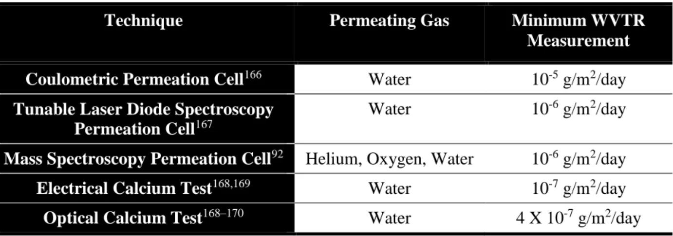
Renewable energy sources have become one of the most important initiatives facing mankind today. Greenhouse gas emissions and geopolitical concerns have created a strong need for the replacement of fossil fuels in energy production, with renewable sources being particularly promising. The abundant energy produced by the sun is an especially interesting solution to this problem since capturing only a small portion of the sunlight which reaches Earth could easily meet global energy demand as illustrated in Figure I.1.1 Accordingly, the amount of solar photovoltaic capacity has risen rapidly in recent years from 3.7 GW globally in 2004 to 100 GW globally in 2012.2 This has corresponded well to the development of less expensive photovoltaic panels which convert sunlight directly into electricity.2 However, the energy and time intensive processes for the production of silicon based photovoltaics limit how inexpensive these devices can become. To drastically decrease the cost of photovoltaic devices, new technologies are needed.
Figure I.1 The total possible energy reserves for various sources are shown compared to the total global yearly energy use from 2009 (orange circle). For non-renewable sources, the total recoverable reserves are shown. For renewable sources, the maxium possible energy which could potentially be captured is shown.1
6
While many different photovoltaic technologies have been developed as competitors to silicon-based systems, organic photovoltaic (OPV) devices represent a particularly interesting alternative. These devices use organic molecules and polymers as the semi-conducting light absorber material in place of silicon. These devices tend to operate best when the active layer materials are on the order of hundreds of nanometers in thickness. This, combined with the ability of organic materials to be solubilized in solvents, allows for devices to be printed at relatively low temperatures using evaporative deposition techniques or solvent-based inks.3 The thin, non-brittle nature of these active layer materials also allows for devices to be flexible. This flexibility enables the use of low-cost production techniques, such as roll-to-roll processing.3–5 Thin active layers also cause less material to be used. This combination of cost, low-temperature processing and low material usage creates the potential for OPV devices to be much less expensive and with much shorter energy payback times than their silicon-based counterparts.
OPV devices also have several other advantages which increase their utility. By printing devices on flexible foils, the final devices are much thinner and light-weight than silicon modules. Their flexible nature also allows for more creative deployment of the modules onto both curved surfaces and other flexible materials. The ability to print devices also create the possibility for unique custom shapes, further opening the new options for the deployment of the modules. These attributes also combine to make OPV modules ideal for many smaller niche applications such as chargers for devices or for incorporation into other devices such as smart textiles. OPV technologies also often exhibit less loss of power conversion efficiency at sharp angles of incidence and in low light conditions compared to silicon based modules.6 This eliminates the need for expensive solar tracking mounts and makes OPV modules potentially interesting for indoor applications where the illumination is not as intense.
OPV devices do have several drawbacks however. Traditionally, the largest obstacles to large-scale implementation of OPV devices have been their relatively low power conversion efficiencies (PCE)7 and short device lifetimes.8–10 The problem of low PCE has been the focus of much research and lab scale cells have now surpassed 12% PCE.11 This has been achieved primarily through development of better active layer materials and device architectures such as tandem cells. While this PCE is still low compared to other solar technologies, it has become sufficiently high for OPV devices to become commercially viable. Devices fabricated using industrial scale methods are often not as efficient as those at the lab scale,3–5,12,13 but the large
7
number of companies currently in or preparing to shortly enter industrial scale production indicates that this loss of PCE is not drastic enough to prevent their commercialization.11,14–23 The problem of short device lifetimes remains however. This problem stems from the sensitivity of many OPV materials to light, oxygen, water, and combinations thereof. 8–10,24 As a result, much research has been performed to develop more stable OPV materials and high gas-barrier encapsulation materials. This has increased the achievable device lifetimes for OPV devices, but much work remains to reach the level of long-term device stability seen for other solar technologies.10 While flexible multi-layer barrier films can now often meet the oxygen and water vapor transmission rate requirements needed to extend device lifetimes to several years,25 less progress has been made in preventing gas permeation in the adhesives used to seal devices between these films.26 This allows for lateral gas permeation, also known as side ingress, to occur and degrade devices from the edges inward.
The goal of the work presented in this thesis is to better characterize and develop materials to limit the problem of lateral permeation into OPV devices, thus prolonging their device lifetimes. A new testing procedure is presented which aids in the characterization of permeation in OPV devices. This test, a modified form of the optical calcium test, allows for the comparison of multiple permeation pathways in encapsulation schemes, while also providing a tool for the comparison of different encapsulation materials. This modified optical calcium test, along with other established characterization techniques, is then used to develop and evaluate enhanced adhesives with decreased later permeation rates. These enhancements include modification of the adhesives’ formulation and the addition of nanoparticles. Relatively impermeable passive nanoparticles are used to make adhesive nanocomposites as a method to lengthen the permeation pathway by creation of a tortuous pathway. A novel approach using active nanoparticles which bind permeating species is also investigated to create adhesive nanocomposites. The enhanced adhesives are then used to encapsulate OPV cells and subjected to accelerated aging to determine their relative impact on the device lifetimes of OPV devices. Finally, the photostability of the enhanced adhesives is analyzed to ensure the adhesives will continue to function as desired after exposure to light, which is of particular importance for OPV encapsulation materials which can spend years exposed to intense sunlight.
9
Chapter 1: Background
Introduction
In this chapter a bibliographic study of the literature is presented in order to establish a basis for further discussion and to provide an overview of the state of the art in the fields of encapsulation of organic photovoltaic devices, adhesive composites and permeation measurement. With these goals in mind, the principles of how organic photovoltaic devices work are presented along with their primary degradation mechanisms. Next, an overview of common encapsulation materials and how they are used to encapsulate devices is provided. Included in this overview is a discussion of the gas permeation mechanisms associated with each type of encapsulation material. Finally, testing techniques for measuring the low permeability rates found in encapsulation materials is discussed.
Organic Photovoltaic Technologies
Organic photovoltaic devices (OPV), as previously discussed, are a very promising technology to provide low cost electricity. Their use of organic semiconductors gives OPV devices unique characteristics in comparison to other solar technologies. This section aims to illuminate the principles of how these devices produce electricity from light along with how this process can become hindered by the various degradation mechanisms present in the devices. As one of the stated goals of this doctoral research is to improve the lifetime of OPV devices, a current understanding of what limits the device lifetime is crucial.
How OPV Devices Function
Just as with other photovoltaic technologies, OPV devices absorb light which produces an electron-hole pair that is then used to generate a current. Unlike other photovoltaic technologies however, the absorber material in OPV devices is an organic molecule instead of an inorganic semi-conductor. These molecules have a highly conjugated system of molecular orbitals which allows for the creation of a band gap that corresponds well to the energy of visible light.27 The energy levels of the highest occupied molecular orbital (HOMO) and lowest
10
unoccupied molecular orbital (LUMO), and thus the band gap, are determined by the chemistry of the organic molecules. A large variety of absorber materials exist for OPV devices with different band gaps, absorption spectra, π-π stacking, solubility and intrinsic stability.10,27,28 These materials also range in molecular weight from smaller non-repeating molecules to longer chain polymers with examples shown in Figure 1.1. Since the ability of the absorber material to generate electron-hole pairs is of fundamental importance to a device’s ability to generate a photocurrent, much research continues into the development of new absorbers.27
Figure 1.1 The chemcial structures of (a) the small molecule absorber pentecene, (b) the polymeric absorber poly(3-hexylthiopene), and (c) the acceptor phenyl C61 butyric acid methyl ester are shown as examples of commonly used OPV
active layer materials.
Along with the absorber material, the rest of the so called active layer of the OPV is comprised of an electron acceptor material. This material aids in separating the charges of the electron hole pair as its LUMO energy level is carefully selected to create a favorable condition for the transfer of electrons from the absorber to the acceptor. While many different materials are possible for use as an acceptor, the most common materials are based on fullerenes such as the molecule seen in Figure 1.1c.10
Commonly, the absorber material is mixed with the acceptor material to form what is known as a bulk heterojunction structure. Because the two materials are generally immiscible, they phase separate to form micro-domains within the active layer. This greatly reduces the distance between the absorber and acceptor at any given point in the active layer, which is particularly advantageous for OPV as the length scales for geminate recombination are relatively short (~10nm). The morphology of this layer is therefore critical to the overall performance of the device as the domain sizes and distribution can greatly change the amount of recombination which occurs within the active layer. 8,9
11
With the planar nature of most OPV architectures, the active layer is sandwiched between a cathode and an anode to create a functioning photovoltaic cell. However, due to the HOMO and LUMO levels of the active layer materials and the work functions (energy barrier for transfer of electrons at a metallic surface) of the conductive electrode materials, it is often advantageous to include intermediate layers as electron or hole transporters. These layers facilitate the transport of charges from the active layer to the electrodes by providing an energy level which is between that of the active layer and the electrode. These materials can also improve the interfaces allowing for better transport of charges between layers.27 Electron transport layers (ETL) usually consist of a metal oxide such as zinc oxide (ZnO) or titanium oxide (TiO2, TiOx). Hole transport layers (HTL) are commonly made of poly{3,4- ethylenedioxythiophene} blended with poly{styrene sulfonate} (PEDOT:PSS), though inorganic materials such as molybdenum VI oxide (MoO3), tungsten VI oxide (WO3) and vanadium V oxide (V2O5) can also be used.10,29,30
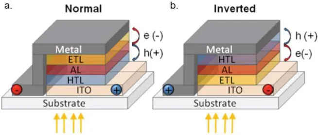
OPV electrodes consist of a transparent front electrode and a metallic back electrode. As there are very few known quality transparent conductors, the majority of OPV devices to date use indium tin oxide (ITO) for the transparent electrode. However, much research has been done to develop alternatives to ITO because of its cost and processing difficulties. Metallic grids and silver nanowires in conductive polymer matrices are two common ITO replacements for the transparent electrode. The transparent electrode is typically coated onto a transparent substrate such as glass or a polymer film.4,10,31,32 This electrode can be either the cathode or the anode depending on the desired architecture of the cell. In a classical structure, the HTL is coated on top of the transparent electrode followed by the active layer, ETL and back electrode. In this architecture, the electronic properties of the cell necessitate the use of a low work function electrode such as calcium or aluminum. In an inverted architecture the cathode and anode are switched (and thus also the ETL and HTL).9,10,25 This results in the ability to use a higher work function material with silver being by far the most common choice. A diagram showing the differences in these two architectures can be seen in Figure 1.2.
12
Figure 1.2 Diagrams of the structure of the (a) classical, or normal, and (b) inverted architectures for OPV are shown.9 One major drawback which has inhibited the widespread adoption of OPV
technologies are their relatively low power conversion efficiencies in comparison to other solar technologies. In recent years the efficiencies of OPV devices have greatly improved however, as can be seen in Figure 1.3.33 This increase in power conversion efficiencies to over 10% has greatly improved the prospects for the commercialization of OPV technologies as evidenced by a number of companies which are nearing industrial scale production of OPV devices. 11,14–23
13
Figure 1.3 The record certified power conversion efficienies for lab-scale solr cells is shown with OPV techonoloies represented by orange circles and triangles. This plot, reprodced here in modified form, is courtesy of the National Renewable Energy Laboratory, Golen, CO, USA.33
Degradation Mechanisms
One of the major problems limiting the wide scale production and deployment of OPV is their instability. The performance of OPV tends to degrade over time and does so quite rapidly in comparison to most other solar technologies. This degradation comes from a combination of different mechanisms at different levels within the device. In fact, there are degradation mechanisms present at almost every material and interface within an OPV device, as can be seen in Figure 1.4.8–10,24,28 Limiting degradation and therefore extending device lifetimes is critical to the adoption of OPV on an industrial scale. In order to develop methods to prevent the loss of performance in OPV, it is necessary to understand its root causes.
14
Figure 1.4 Several different possible degradation pathways for OPV are shown in these cross-sectional diagrams of a typical bulk-heterojunction OPV with (a) a classical structure and (b) an inverted structure. In these images “Polymer” refers to a polymeric active layer absorber material, “PCBM” is a fullerene based electron acceptor material and P3HT is the active layer absorber material poly(3-hexylthiophene).8,10
Starting at the active layer, several different degradation pathways exist.8–10,28,34 The light absorbed by the electron donor material not only produces electron-hole pairs for electricity generation, but can also cause intrinsic degradation. The photostability of active layer
15
materials varies greatly as many different types of molecules with different chemistries can be used, however most will undergo some form of photo-degradation. This degradation can take the form of oxidation of the macromolecular chains, chain scission or cross-linking, but in any case the photo-degradation results in a modification of the electronic structure of the molecules thereby affecting the absorption, charge generation and charge transport of the active layer. While photolysis reactions will occur without the presence of oxygen, they tend to be at a relatively slow rate compared to the faster kinetics of the photo-oxidative reactions. An example of this is found in the common OPV absorber material poly(3-hexylthiopene) (P3HT) which shows very good photostability in photolysis conditions where no oxygen is present while showing pronounced degradation in photo-oxidative conditions in air. 10,28,34,35 Therefore, limiting the presence of oxygen in the active layer can improve its stability. However, this result does not hold true for every active layer material with some materials, such as (MDMO-PPV), showing relatively poor photostability even when oxygen is not present.10,28,34 Also, the overall level of photo-degradation can be limited by the use of UV screening encapsulation as the higher energy UV light generally degrades the materials at a faster rate than visible light, though the materials will also degrade from visible wavelengths.10,26
Non-photo-induced degradation can also occur in the active layer. Oxygen and water can react with the active layer via other reaction routes even under dark conditions, making their exclusion even more important.10 The active layer can also be responsible for changes in performance over time due to the nature of the bulk heterojunction structure. Since the active layer is a mix of two immiscible materials, phase domains form. These domains are critical to the proper functioning of the device in terms of charge separation and conduction of charges towards the electrodes. However, the morphology of these domains is not thermodynamically stable in most cases and can therefore change over time. Changes to the active layer morphology are generally thermally activated processes and can cause changes in device performance by increasing the distance charges must travel to reach the acceptor material. This leads to an increase in recombination as fewer electron hole pairs are effectively separated. Changes in the morphology can also lead to changes in the concentration of each phase at the interfaces with the adjacent layers which can affect the charge transfer to these layers.10 Additionally, fullerenes, which are commonly used as the acceptor material in the active layer of bulk heterojunction devices, tend to have very low surface energies making adhesion to adjacent layers difficult. This weak adhesion makes delamination more likely when mechanically stressed.10,36,37
16
The intermediate charge transport layers can also contribute to the loss of performance in OPV.8–10,29 Many of the metal oxide materials used as electron transport layers can act as photo-catalysts by aiding in the formation of oxygen radicals when molecular oxygen is present. These radicals are then able to attack the adjacent organic active layer.8–10,34 These metal oxides can also react with oxygen to form superoxides which create electron trap states.10 Hole transport layers, in particular PEDOT:PSS, can contribute to the degradation of OPV. PEDOT:PSS is a very hygroscopic material and can speed the permeation of water throughout the device and act as source of water for other degradation processes in adjacent layers.10 PEDOT:PSS is also acidic in nature and can etch ITO over time in devices using the classical structure where the two materials are in contact, especially when water is also present.8,10 Additives and surfactants in commercial formulations of PEDOT:PSS can also diffuse to the surfaces of the layer and affect the interfaces with adjacent layers. 8,10
The transparent electrode can also cause a loss of device performance. Traditionally, the vast majority of OPV have used ITO for this layer. ITO is a brittle material however and is prone to cracking when flexed.10 Indium from the electrode can also diffuse throughout the rest of the device.8,10 As ITO also has several other processing concerns, replacements for ITO have been an active area of research. While other metal oxides have been considered for use in place of ITO, metal grids and silver nanowires are currently the most prevalent alternatives to TCOs, but both are usually embedded in a conductive polymer to form the electrode.4,10,31,32 The most common polymers for this task are high conductivity PEDOT:PSS formulations and therefore these electrodes tend to exacerbate the previously discussed degradation mechanisms associated with PEDOT:PSS.38
The stability of the metal back electrode depends greatly on the architecture of the device.9,10,25,39 For classical structures, this can be one of the most sensitive materials in the device. For optimal electrical performance, metals such as aluminum and calcium are used. However, both of these materials are unstable in air. Aluminum can oxidize to form an electrically insulating layer at the interface where it is in contact with the device. Additionally, aluminum can react with and diffuse into fullerene layers when no intermediate layer is present.8,10 Calcium meanwhile is highly reactive with water to form the non-conductive calcium hydroxide.8,10 Using an inverted structure, these highly reactive metals can be replaced with the much more noble silver. This change in electrode material is credited as the reason why the inverted structure is several orders of magnitude less sensitive to water ingress as seen in Figure 1.5. 9,10,25,40
17
Figure 1.5 Plots of aging of OPV cells at 38°C and 100% relative humidity under illumination are shown as a function of the mass of water which had permeated across the encapsulation for both (a) classical and (b) inverted architectures. The inverted cells maintained 50% power conversion efficiency with 2 orders of magnitude more water present inside the encapsulation.25
While many different materials are used throughout each layer of OPV devices, it can be seen that light, temperature, oxygen and water play significant roles in the loss of device performance. Photo and thermal degradation processes are more difficult to avoid and generally must be addressed by improvements to the materials and device architectures. Oxygen and water on the other hand, can be limited through the use of high gas barrier encapsulation. The elimination of these contaminants from the device can greatly improve the device lifetime without the need to modify the device itself.10,26
Similar Technologies
While the main focus of this thesis is on the application of OPV, the same types of permeation testing, barrier materials and encapsulation techniques are also applicable to other technologies. The most similar analogous technologies are other organic electronic devices, but other types of inorganic solar technologies can also benefit from improved high-barrier encapsulation.
Organic electronics are a large class of devices, which include OPV, that use organic semiconductors to create electronic devices. All organic electronics are susceptible to the inherent instability of organic semiconductors compared to highly stable inorganic semiconductors. Some types of devices are more stable than others however. For example, organic thin film transistors are generally more stable due to their lack of illumination and an
18
architecture which usually incorporates an inorganic insulating material which provides some barrier protection.41–43 On the other hand, some organic electronics are as, or more, vulnerable than OPV. Organic photodetectors are one such device which use the photovoltaic effect of organic semiconductors to sense the presence and/or intensity of light. These devices are constructed using device architectures very similar to those of OPV but are optimized differently in order to achieve more sensitive measures and clearer on/off signals. Although the operational conditions are different from OPV (indoor vs. outdoor, different spectra of illumination), they are nonetheless subject to the same degradation mechanisms as OPV.13 Another analogous organic electronic technology is the organic light emitting diode (OLED). Organic light emitting diodes operate in a manner similar to inorganic light emitting diodes in that they luminesce at certain wavelengths when subjected to an electric potential. While some of the materials used are slightly different than in OPV, they generally have device architectures which are nearly identical to those of OPV. This makes them vulnerable to all of the same degradation mechanisms as OPV. In addition, OLEDs usually have much poorer performance with inverted architectures, therefore most OLED devices use a classical architecture with easily degraded, low work function electrodes. This makes them even more sensitive than OPV and the generally recognized maximum water vapor transmission rate (WVTR) for OLED encapsulation is 10-6 g/m2/day compared to 10-3 g/m2/day for OPV.25,44–51 It should also be noted that OLEDs have different requirements for what constitutes a failed device as point defects such as dark spots are often considered unacceptable for OLED displays but are not a major concern for OPV which is concerned mainly with the total amount of energy harvested.
Other photovoltaic devices are also vulnerable to degradation from permeating gases and require barrier encapsulation. The prominent degradation mechanisms of several types of solar technologies are shown in Figure 1.6.10 Crystalline silicon modules are intrinsically very stable devices, however they still require encapsulation to avoid mechanical fracturing of the silicon and corrosion of the metal electrical connections. Preventing corrosion of the electrical connections requires only minimal barrier protection though and crystalline silicon modules are able to achieve very long device lifetimes using encapsulation materials with relatively high permeation rates such as poly(ethylene-co-vinyl acetate) (EVA).10,52,53 Thin film photovoltaics are much more susceptible to degradation than crystalline silicon modules, however they are still less sensitive than OPV. Amorphous silicon modules can suffer from photo-degradation of the active layer, however this has been mostly controlled through better control of the nano and micro crystallinity of the silicon.10 Cadmium telluride based modules can suffer from degradation due to the back electrode which can diffuse into the active layer or corrode in the
19
presence of humidity. This has largely been solved through the use of more stable electrode materials such as antimony-molybdenum alloys and encapsulation with relatively high permeation rate materials such as (EVA).10 The most sensitive inorganic photovoltaic modules are those which use a copper indium gallium diselenide (CIGS) active layer. This sensitivity comes primarily from the degradation of the Al:ZnO front electrode in the presence of humidity. While the traditional encapsulation techniques used for crystalline silicon modules can work for CIGS modules, they are not always sufficient water barriers for long device lifetimes. CIGS encapsulation is further complicated by their ability to produce flexible modules which cannot use impermeable glass sheets. This creates an encapsulation problem very similar to that of flexible OPV, though CIGS barrier requirements are less strict.54–60 Nonetheless, encapsulation technologies developed for flexible OPV are directly applicable to flexible CIGS modules as well. Recently, rapid advances have been made in organic-inorganic hybrid photovoltaic cells based on a perovskite structure with laboratory-scale cells showing power conversion efficiencies of up to 22%. While the materials and device physics are quite different for these materials as compared to OPV devices, they provide many of the same benefits as OPV devices including low-temperature processing, the use of printable inks, and the mechanical flexibility of the devices.61–65 The stability and degradation mechanisms in these perovskite cells are still being investigated. It does appear that some type of flexible encapsulation will also be needed for this technology although it may still be too early to tell what level of gas barrier protection will be needed.
20
Figure 1.6 Cross-sectional diagrams along with the most prominent degradation mechanisms are show for solar cells with active layers based on (a) crystalline silicon, (b) amorphous silicon, (c) cadmium telluride and (d) CIGS. Images modified from Krebs et al. 10
21
Permeation Mechanisms and
Encapsulation Materials
Permeation Mechanisms in Materials
Fickian Diffusion
Fick’s Laws of diffusion were first published by Adolf Fick and provide a mathematical model of diffusion. Fick’s First Law describes the flux of permeating species through a matrix as a function of the spatial concentration gradient as is seen in Equation 1.1 for the case of one dimensional diffusion.66
Equation 1.1 𝐽 = −𝐷 𝜕𝐶 𝜕𝑥
In this equation J is the flux, D is a permeant and material dependent constant known as the diffusion coefficient, C is the concentration of the permeating species and x is the distance in the direction of diffusion. The diffusion coefficient, D, is a function of temperature with an Arrhenius type relation as seen in Equation1.2.66
Equation 1.2 𝐷 = 𝐷𝑜 𝑒−𝐸 𝑅𝑇⁄
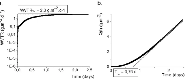
In this equation E is an activation energy which is constant for a given material, R is the universal gas constant and T is the absolute temperature. Fick’s First Law is particularly useful for modeling diffusion in the steady state. Steady state diffusion can be defined as a case where the spatial concentration gradient is constant resulting in a constant flux. Before achieving a steady state condition, the permeation is in the transient state. In this state, the concentration gradient within the material changes as a function of time.66 This can be seen in Figure 1.7 which shows the stabilization time needed for the permeation of water vapor for a typical barrier material.25
22
Figure 1.7 Plots for the water permeation of a flexible tri-layer laminate of polyethylene (46μm) – ethylene : vinyl alcohol copolymer (6μm) – polyethylene (46μm) are shown as measured by a mass spectrometry based permeation cell using heavy water. (a) The WVTR of the material increases throughout the transient state until stabilizing to a constant value after approximately 1.5 days signifying that the steady state has been achieved. (b) When plotted as a cumulative mass of permeated water, Q, the time lag, TL, can be calculated by extending a linear fit of the steady state region back to
Q=0.25
The amount of time needed for the significant amounts of gas to permeate across a barrier can be estimated as the time lag (TL). The time lag is found by extending the linear, or steady state, portion of a plot of mass permeated versus time until it crosses the time axis. The value of time at the point along this linear curve where the mass permeated is 0 is defined as the time lag as illustrated in Figure 1.7b. This value, h2/6D where h is the thickness of the film, can be obtained from the linear part of the curve Q=f(t), which is obtained by the resolution of the second Fick’s law in the steady state regime. For barrier films, the barrier properties against a certain gas must therefore be reported with both a steady state permeation rate and the time lag in order to accurately predict the total permeation. Also, due to the temperature sensitivity of D, these two values are only valid for a given temperature.25,66–68 Figure 1.8 shows an example of how these two values can be used to predict whether a material can meet the barrier requirements for a certain application.25
23
Figure 1.8 (a) Isochrones are plotted which correspond to the time required for a mass of 1 g/m2 to permeate across a
film. It should be noted that for short time lags, the permeation is dominated by the WVTR. However, as the time lag approaches the desired lifetime, the time lag becomes the dominant parameter. A homopolymer film, polymer laminate film and a polymer laminate with an inorganic barrier layer are also plotted as points. (b) If the quantity of permeant required to cause failure in a device is known, isochrones can be plotted for device lifetimes. Isochrones for classical and inverted OPV cells are shown in conjunction with the three example barrier films. If the point representing the barrier film is below/right of the isochrones, it will provide sufficient barrier protection to achieve the desired device lifetime.25
For Fickian diffusion, the transient state can be modeled using Fick’s Second Law which relates the change in the spatial concentration gradient with the temporal change in concentration as seen in Equation 1.3.66
Equation 1.3 𝜕𝐶 𝜕𝑡 = 𝐷
𝜕2𝐶 𝜕𝑥2
One important solution to this differential equation is for the case of one dimensional diffusion into a semi-infinite material. For this case, the steady state is never achieved as the leading edge of the diffusion front never reaches the opposite side of the material. Solving using these boundary conditions yields Equation 1.4 where erf is the error function, Co is the concentration at the exposed edge of the material and A is a constant.52,66,69
Equation 1.4 𝐶 − 𝐶𝑜 = 𝐴 𝑒𝑟𝑓 ( 𝑥 2(𝐷𝑡)1/2)
By selecting a particular concentration, the difference C – Co becomes a constant meaning the operand of the erf must also be constant. This allows for the characterization of the advancement of the diffusion front, which is seen in Equation 1.5, where K is a material constant valid for a particular temperature and concentration.52,66,69
Equation 1.5 𝑥 = 𝐾 𝑡1/2
Polymeric Barrier Materials
24
Polymers are an excellent example of materials which follow Fick’s Laws. The chain-like nature of polymers creates a large amount of free volume when compared to other dense solids. This free volume allows gases to permeate relatively easily through most polymers.70 Reduction of the free volume through crystallinity and crosslinking can help to limit the permeability to an extent. 70 Polymers are commonly used as barrier materials for applications such as food packaging and a list of the oxygen transmission rate (OTR) and water vapor transmission rate (WVTR) for various polymers used for barrier applications can be found in Figure 1.9.26,71 As can be seen in this figure, even the best polymeric barriers remain several orders of magnitude higher than the OPV requirements of 10-3cm3/m2/day/bar and 10-3g/m2/day for OTR and WVTR respectively.
Figure 1.9 The permeation rates for oxygen and water vapor of various polymeric barrier materials are plotted. The colored regions of the plot correspond to the barrier requirements for various applications. It should be noted that this plot was published before the popularization of the inverted structure for OPV, therefore the OPV region on the plot could be extended to 10-3 g/m2/day on the water vapor transmission rate axis based on more current estimations.71
Inorganic Barrier Materials
Dense inorganic materials also display Fickian diffusion behavior in defect free regions. However, unlike polymers, the more tightly packed chemical structure of these materials greatly reduces their permeation rates. In fact, for many inorganic materials Fickian diffusion is so slow that they are effectively impermeable to oxygen and water at room temperature. This makes these materials prime candidates for barrier applications. Thin metallic coatings are
25
frequently used to improve the barrier properties of polymer films, however their opacity makes them ill-suited for use in the optical path where transparency is required. The best example of a transparent inorganic material displaying Fickian permeation is silica glass. The large thickness of glass sheets prevents the presence of defects which could traverse the sheet. This makes sheets of glass effectively impermeable to oxygen and water in the temperature range seen for outdoor applications.72 Glass has indeed been widely used to encapsulate OPV and other even more sensitive devices. However the thickness of glass required to provide effectively impermeable encapsulation generally results in rigid devices.10,26 While somewhat thin films of flexible glass can be used, they often remain relatively brittle and thus easily form large defects which gases can penetrate.73,74 For silica and other metal oxide materials to be highly pliable for use in flexible encapsulation, the thickness must be reduced to such a level that defects become unavoidable. This makes their permeation no longer Fickian and instead completely dependent on the density and size of the defects.75,76
Defect-Dominated Permeation and Tortuous Paths
For the relatively thin layers of no more than several hundred nanometers required to make rigid inorganic materials flexible enough for use in flexible encapsulation, it becomes unavoidable to incorporate defects with almost all current technologies.75 These defects traverse the thickness of the material and provide a much easier permeation pathway for gases. These defects can include cracks from mechanical stresses, deposition inhomogeneities, grain boundaries and nanoporosity. The presence of these defects across the thickness of an otherwise impermeable layer greatly changes its effectiveness as a gas barrier. This means that the overall permeation can no longer be described by Fick’s Laws but is instead dominated by the relatively rapid permeation across the inorganic layer via defects. It has been shown that the permeation rates for thin layers are strongly dependent on the size and density of defects.68,76
Commonly used inorganic materials for these thin, flexible barrier layers include SiO2, Al2O3, TiO2, Zr2O3, Zn2SnO4 and SiN as they are generally able to produce the best quality films in terms of defects. Many different deposition techniques can be used to create these films but there is always a balance of film quality, processing time and cost which has thus far prevented any one technology from gaining a large advantage over the others. Current deposition techniques include reactive sputtering, plasma enhanced chemical vapor deposition, atomic layer deposition and photo-conversion of liquid ceramic precursors.43,71,75,77–85 In order to minimize the probability that a defect will traverse the thickness of the material, thicker layers
26
are preferred. However, the brittle nature of these materials causes thicker films to be prone to cracking from mechanical and thermal stresses. Therefore a minimum permeation rate is usually obtained with a thickness in the range of 50-150nm as can be seen in Figure 1.10.75,77 However the permeation rates achieved at these thicknesses are still too high to achieve the requirements of OPV. Only atomic layer deposition has been shown to be capable of creating acceptable gas barrier protection for OPV devices with thicknesses below this range.45–47,71,81,86– 89 However, there are currently other drawbacks to this process which will be discussed later in this chapter in the “Encapsulation Techniques” section.
Figure 1.10 The OTR of SiOx layers of various thicknesses deposited on PET are shown for various deposition techniques. Thicker layers limit the number of defects which completely traverse the SiOx layer, however very thick layers become less mechanically stable and prone to cracking. This results in a minimum OTR at an SiOx thickness in the range of 50-150nm.75
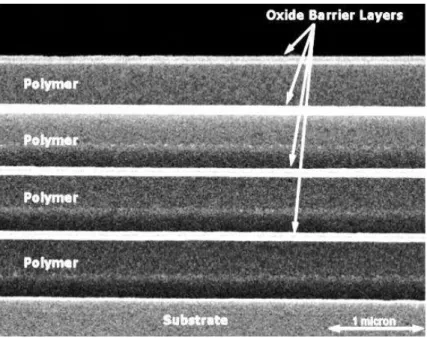
In order to further improve the barrier properties of inorganic materials with defect-dominated permeation, multilayer systems have been employed. The goal of a multilayer system is to create stacks of inorganic barrier layers and therefore improve the barrier performance without cracking from stresses. This has been achieved by using softer intermediate layers in between the inorganic layers. Beyond providing more mechanical stability to the inorganic layers, this structure also creates discontinuities between the defects in each inorganic layer. The result is a so called tortuous path for the permeation of gases. After traversing a defect in an inorganic layer, the gas must then permeate along the next inorganic
27
layer until another defect allows for the gas to traverse the layer as shown in Figure 1.11. The increased path length for permeation caused by this tortuous path greatly enhances the barrier properties of the stack. A combination of one barrier layer and one intermediate layer is known as a dyad and reductions of the OTR and WVTR by multiple orders of magnitude have been reported for stacks with as few as two dyads.10,26,50,68,71,85,90–94
Figure 1.11 The black arrows represent possible permeation pathways through a three dyad multi-layer barrier film. These pathways are tortuous as the permeating molecules cannot traverse the laminate in a straight line. Instead, the gas must permeate through each intermediate polymer layer along the impermeable inorganic barrier layers until it reaches another defect. This greatly increases the path length for permeation and therefore results in a low permeation rate.92
Passive Composite Barrier Materials
The intermediate layers in a dyad structure are designed primarily to provide a planar layer for the next inorganic barrier deposition while breaking the transfer of defects from one barrier layer to the next. This is most commonly achieved through the use of an organic polymer which can be coated to a thickness on the order of microns.26,68 The relatively soft nature of polymers provide some stress relief to the brittle barrier layers, especially from the thermal stresses as many deposition techniques require elevated temperatures. They are generally not intended to serve as barrier layers themselves. However, an intermediate layer with some inherent barrier properties could slow the permeation rate of the multilayer stack even further as any permeating gas must pass through this material. With this goal in mind, several alternative intermediate layers have been proposed in the literature including heavily cross-linked organic polymers, composites of organic polymers and inorganic particles, and inorganic polymers.71,85,90,91,95–97 In addition to intermediate layers, it is often necessary to use an adhesive of some kind to secure a barrier stack or other encapsulation material to the device being encapsulated. Improving the barrier properties of these adhesives is also critically important as they are often present in much thicker layers than the intermediate dyad layer and can be a weak link in some encapsulation processes, which will be discussed in detail later in this chapter. These adhesives therefore have quite similar requirements to the intermediate layers of a multi-layer barrier and often use the same strategies to reduce their permeation rates.94–102
28
The concept of the tortuous path can also be applied to polymeric systems through the incorporation of inorganic particles. By dispersing particles made of a relatively impermeable material throughout the polymer, any permeating gas must go around the particle. The resulting increase in the permeation path length is a tortuous path just as in the case of the previously discussed stacks of thin inorganic layers. Since the particles simply block the path of permeating gases and do not strongly interact with them either through sorption or chemical processes, this type of composite material is said to be passive in nature. The barrier effect caused by the introduction of passive particles is well known and has been heavily exploited for many years using a wide variety of particles. Commonly used particles include but are not limited to SiO2, Al2O3 and TiO2. These particles are often on a length scale of several microns or greater and are incorporated at high concentrations to achieve low permeation rates. However, high concentrations of these materials limit or eliminate the transparency of the composite and can often cause the composite to be quite rigid which causes any encapsulated device to lose its flexibility. Decreasing the concentration of particles shortens the tortuous path however and thus leads to high permeation rates. The large size of these particles also limits the minimum thickness of a layer of the material and can lead to a less planar surface.70,90,97,103–106
To solve the problem of reducing the mass or volume fraction of particles while maintaining a tortuous permeation path, it quickly becomes apparent that a high aspect ratio particle is needed. A plate-like structure with a large diameter and small thickness should be able to provide a tortuous path even at low loadings. This has led to the widespread use of phyllosilicate particles in passive composite barrier materials. Phyllosilicates are silicate materials which also incorporate other cations into their tetrahedral bonding structure. The tetrahedrons are organized in manner that forms strong covalent bonds in two dimensions but relatively weak bonds in the third dimension resulting in a plate-like structure. A diagram of the structure of the phyllosilicate material montmorillonite is shown in Figure 1.12 as an example of this type of structure.107 When properly dispersed in a solution or polymer, the plates become exfoliated and the thickness of each individual particle becomes the thickness of a single plate. This results in a particle with a diameter on the order of several microns and a thickness of only a few nanometers. To more effectively exfoliate phyllosilicates dispersed in polymers, they are often organically modified using salts with short organic chains covalently attached. These very high aspect ratio nanoparticles are able to provide a tortuous permeation path at loadings of just a few weight percent thus preserving the transparency of the composite.90,91,103–106,108–114
29
Figure 1.12 A diagram of the structure of montmorillonite is shown. Like other phyllosilicates, montmorillonite consists of sheets of tetrahedrally and octahedrally coordinated silicates. Between each sheet are cations and absorbed water. If the particles have been organically modified the organic salts would also occupy this space between sheets. When exfoliated, the sheets separate creating particles with a very high aspect ratio.107
Getters
An alternative approach to the passive composite and tortuous path is the use of an active material which strongly interacts with a permeating gas. These active materials are commonly known as getters and can be broken into two major classes: those who consume a permeating gas through a chemical reaction; and those who trap permeating gas via sorption processes. Depending on the exact type of getter used, they can either be incorporated into polymer as a composite or placed inside a cavity with the device to be protected. By definition, a getter must interact with the permeating gas, therefore many getters are developed to interact with one particular gas. Getters which are designed specifically for water are often referred to as desiccants.
Reactive
Reactive getters consume permeating gas via a chemical reaction, thus eliminating the gas. These getters have traditionally been used in vacuum tubes in order to eliminate any contaminates which might degas over time in the tube. Though many different materials have been used as reactive getters, they are usually based on highly reactive metals such as barium, zirconium alloys and calcium or sometimes their intermediate reaction products (i.e. CaO which is an intermediate product in the reaction of Ca and water to ultimately form Ca(OH)2). Some types of reactive getters, such as CaO, can also be prepared as particles and incorporated into composite materials.26,47,48,115
30
Sorption
Rather than consume any permeating gas, some getters instead adsorb the gas molecules on their surface. As these materials need a high surface area to adsorb large quantities of gas, they are usually highly porous often with pore diameters on the order of only a few nanometers. Several common types of getters which use adsorption are silica gels, activated carbon, templated mesoporous materials and molecular sieves such as zeolites and aluminophosphates. Silica gels (aerogels, xerogels) have the highest water sorption of these materials due to the high porosity produced by their sol-gel processes. These materials take advantage of the ample silanol groups on their surfaces to bind polar water molecules. Templated mesoporous materials are also usually silicates or aluminosilicates which have been assembled into a mesoporous structure with the aid of organic surfactants which phase separate on nanometer length scales. Despite their high water sorption capabilities, these materials are often relatively expensive to fabricate and can have problems with long term stability. Zeolites are aluminosilicates which have an ordered highly porous structure that allows for a high water sorption capacity, though slightly lower than silica gels. Aluminophosphates are very similar to zeolites except that they are based on phosphate chemistry instead of silicates. These materials can have higher water sorption than zeolites but are generally less stable and more expensive. A comparison of some of the properties of these materials can be found in Table 1.1. Most of these materials are typically fabricated into particles on the micro-scale or larger, which severely limits their ability to maintain transparence when dispersed into a composite, especially activated carbon which strongly absorbs visible light.105,106,116–118
Table 1.1 Comparison of different materials for water sorption Material Water sorption
capacity (g/g)
Water sorption rate
Price Long term stability
Silica Gels 0.40 – 1.45 Medium Medium High
Templated Mesoporous Materials
0.45 – 0.84 Medium High Low
Zeolites 0.20 – 0.45 High Medium High
Aluminophosphates 0.15 – 0.54 Medium High Low
Of particular interest are zeolites as they have the ability to be manufactured as nanoparticles. There are a wide variety of zeolite structures, but they are generally based on cage-like structures created by silicate and aluminosilicate tetrahedra. These cages form a series
31
of ordered pores with the smallest pore diameters in the range of 6-14nm. Water can adsorb on the structure via several different processes. Cations, such as aluminum, can create both Brønsted and Lewis acid sites which are capable of binding multiple water molecules. In addition, clusters of silanol groups within the pores create nests which can bind water molecules and other silanol groups present on the outer surface of the particles also provide sites to bind water. A diagram of these different binding sites can be seen in Figure 1.13.116–118 Nanoparticles of zeolites have been well researched, however their use in barrier composites has received only very limited attention.49,118
Figure 1.13 The different types of water binding sites are shown in the pore structure of a zeolite with an H-MFI structure. B refers to a Brønsted acid site. L refers to a Lewis acid site. N refers to a nest of SiOH groups. And S refers to a surface SiOH group. In this image, the B, L, and N sites are located within the pores of the zeolite.116
Interfaces
When two different materials meet to form an interface, a new permeation pathway can be created which does not follow Fick’s Laws.119–122 Permeation along interfaces is often controlled by the surface energies of the materials and can occur both along the interface itself and/or in within one or both of the materials in the region immediately adjacent to the interface known as the interlayer.
Delamination
When permeation occurs along the interface itself, the result is often a delamination of the interface. Depending on the types of materials meeting at the interface and the type of permeant, this process can occur in different ways. In some cases, the sum of surface energies
32
of material A-to-permeant and material B-to-permeant is lower than the surface energy of material A-to-material B. When this occurs, the system’s preferred state is delaminated and the change in surface energies becomes a driving force for delamination.103,104,123–125 When at least one surface is metal and the permeant is water, galvanic corrosion can occur using the water as an electrolyte which greatly changes the surface chemistry at the interface leading to delamination.103,104 Another mechanism which can cause delamination when water is the permeant is osmotic pressure. As water molecules fill the region between the two materials, the osmotic pressure created pushes the two materials apart and promotes the spread of the delamination along the interface. As the interface delaminates, more water enters the crevice and continues to apply osmotic pressure thus further propagating the delamination. This type of delamination can often be modelled as a mechanical crack growth in a solid material.126–129 Regardless of the type of delamination, access to the interface due to a lamination defect or mechanical stresses can greatly accelerate the start of delamination.
Interlayer Permeation
Even without complete delamination an interface can still provide a rapid permeation pathway. This can occur due to the effects of the interlayers. The region within each material which is immediately adjacent to the interface often has a structure which is different than the bulk material due to the presence of the interface. This modification of the structure can sometimes lead to a faster permeation rate in this region compared to the bulk material and thus increase the overall permeation rate.119,122,124,130 A different but common scenario which occurs in interlayer permeation is a surface energy effect. It is common for a saturated material to have a different surface energy than the same material with no concentration of permeant. If the surface energies favor an interface with the saturated material, this can create a driving force for more permeation in the interlayer.121,123 Conversely, if the interlayer is already saturated due to permeation in the bulk material, the interface can often times become much weaker due to the change in surface energy between the saturated and unsaturated material. This can increase the risk of delamination which would in turn cause more permeation along the interface.127–129
Encapsulation Processes
As previously discussed, the sensitivity of OPV devices to light, oxygen, water and combinations thereof requires that the devices be encapsulated in order to achieve economically viable device lifetimes. Many different encapsulation processes and schemes have been
33
proposed for this purpose and this section aims to provide an overview of the most prominent among these. Regardless of the encapsulation scheme, there are two main permeation pathways which will heretofore be referred to as orthogonal and lateral permeation respectively. Orthogonal permeation is defined as permeation which occurs orthogonally to the plane of the device. Lateral permeation on the other hand, refers to permeation in the plane of the device. Lateral permeation is also commonly referred to as side ingress. A diagram showing these two main permeation pathways can be seen in Figure 1.14. Due to the inherent aspect ratio of OPV devices (large area, small thickness), most encapsulation schemes employ some form of a stack with the device in the center.10,26 This creates interfaces which can provide permeation pathways in the lateral direction. Therefore, the lateral permeation can often be further broken down into bulk permeation through a material and permeation along the interface.
Figure 1.14 The different permeation pathways for water and oxygen are shown on a cross-sectional diagram of a typical encapsulation scheme for OPV. The lighter green arrows show orthogonal permeation while the darker green arrows indicate lateral permeation which can occur in either the bulk adhesive or along the interfaces.
Rigid Encapsulation
As previously discussed, silica glass is an ideal encapsulation material for solar applications as it is both highly transparent and impermeable to oxygen and water under outdoor conditions. As such, this material has been widely used to encapsulate OPV. Glass-to-glass encapsulation is a process which has been carried over from the industrial scale encapsulation of crystalline silicon solar modules. This technique seals the device between two plates of glass using an encapsulant adhesive. The device may be fabricated on its own substrate or directly