HAL Id: hal-02574632
https://hal.archives-ouvertes.fr/hal-02574632
Preprint submitted on 19 Oct 2020
HAL is a multi-disciplinary open access
archive for the deposit and dissemination of
sci-entific research documents, whether they are
pub-lished or not. The documents may come from
teaching and research institutions in France or
abroad, or from public or private research centers.
L’archive ouverte pluridisciplinaire HAL, est
destinée au dépôt et à la diffusion de documents
scientifiques de niveau recherche, publiés ou non,
émanant des établissements d’enseignement et de
recherche français ou étrangers, des laboratoires
publics ou privés.
perpendicular shape anisotropy magnetic tunnel
junctions
N. Caçoilo, S. Lequeux, N. Strelkov, Bernard Diény, Ricardo C. Sousa, N. A.
Sobolev, Olivier Fruchart, Ioan Lucian Prejbeanu, L. D. Buda-Prejbeanu
To cite this version:
N. Caçoilo, S. Lequeux, N. Strelkov, Bernard Diény, Ricardo C. Sousa, et al.. Magnetization reversal
driven by spin-transfer-torque in perpendicular shape anisotropy magnetic tunnel junctions. 2020.
�hal-02574632�
Magnetization reversal driven by spin-transfer-torque in
perpendicular shape anisotropy magnetic tunnel junctions
N. Caçoilo
1, S. Lequeux
1, N. Strelkov
1,2, B. Dieny
1, R. C. Sousa
1, N. A. Sobolev
3, O. Fruchart
1, I. L. Prejbeanu
1and
L. D. Buda-Prejbeanu
11Univ. Grenoble Alpes, CEA, CNRS, Grenoble-INP, SPINTEC, 38000 Grenoble, France 2Department of Physics, Moscow Lomonosov State University, Moscow 119991, Russia
3I3N, Departamento de Física, Universidade de Aveiro, 3810-193, Aveiro, Portugal
The concept of perpendicular shape anisotropy spin-transfer-torque magnetic random-access memory (PSA-STT-MRAM) consists of the increase of the storage layer thickness to values comparable to the cell diameter, to induce a perpendicular shape anisotropy in the layer. Making use of that contribution, the downsize scalability of the STT-MRAM can be extended towards sub-10 nm technological nodes, thanks to a reinforcement of the thermal stability factor 𝚫. Although the larger storage layer thickness improves 𝚫, it negatively impacts
the writing current. Hence, optimization of the cell dimensions (diameter, thickness) is of utmost importance for attaining a sufficiently high 𝚫 while keeping a moderate writing current. Micromagnetic simulations were thus carried out for different pillar thicknesses, with
a square cross-section of fixed size 20 nm. The dependence of the switching time and the reversal behavior was analyzed as a function of the applied voltage. Below a thickness threshold of 50 nm, the magnetization reversal occurs by a collective buckling-like mechanism. Above that threshold, a transverse domain wall is nucleated at the surface near the insulator and propagates along the vertical axis of the pillar. It was further observed that the inverse of the switching time follows a linear relation with the applied bias voltage. This dependency remains linear when considering thermal fluctuations.
Index Terms— Micromagnetism, Perpendicular Shape Anisotropy, Spin-Transfer-Torque, Transverse domain wall
I. INTRODUCTION
The spin-transfer-torque magnetic random-access memory (STT-MRAM) is one of the most promising emerging volatile memory technologies [1]-[4]. It combines non-volatility with a quasi-infinite write endurance, high speed, low power consumption and scalability [5]-[7]. These properties are making STT-MRAM about to enter in mass production for replacing e-FLASH and L3 SRAM [7]-[11]. While initial STT-MRAM devices used an in-plane (IP) magnetization, it has been shown that a perpendicular orientation of the magnetization leads to a better tradeoff between thermal stability factor Δ (related with the memory retention time) and switching current. These devices called perpendicular STT-MRAM (p-STT-MRAM) use the interfacial perpendicular magnetic anisotropy (iPMA) originated at the FeCoB layer and MgO tunnel barrier interface [1], [5], [12]. Nonetheless, there are still some major challenges, predominately when the MTJ goes to sub-20 nm diameters. As the device lateral size shrinks, there is a decrease in Δ due to a decrease in the storage layer volume. This decrease significantly reduces the retention time of the memory [13]-[15]. This limitation can be understood considering that at these small sizes the reversal of the magnetic volume is almost coherent, and so Δ is proportional to the layer volume. In addition, as the surface area shrinks, the iPMA decreases proportionally to the area, until a point where it becomes too weak to stabilize the magnetization perpendicularly. A proposal to counter this decrease is the use of a double FeCoB/MgO interface, by doubling the iPMA [16], [17]. Still, it is very challenging to keep Δ > 60 at sub-20 nm diameters. A promising solution to this problem is a novel concept that takes advantage of the shape anisotropy of the storage layer by increasing its thickness (L) to values of the order or larger than
the cell diameter. Thereby, the shape anisotropy is no longer easy-plane but becomes out-of plane, reinforcing the iPMA to further stabilize the magnetization in a perpendicular orientation. This concept of memory, named perpendicular shape anisotropy STT-MRAM (PSA-STT-MRAM), had been for the first time studied and experimentally developed simultaneously by SPINTEC [18]-[20] and Tohoku University [21]. Later, other groups have published additional works [22]-[24]. As the thickness of the storage layer increases, the magnetization is expected to be more stable due to the large total shape anisotropy [18-21]. However, the current necessary to reverse the magnetization increases consequently. Therefore, for further stack development of these devices, it is important to adjust Δ around the required value specified for the memory operation (typically in the range 60-100) and to keep the switching current as low as possible. For this purpose, the understanding of the magnetization reversal mechanism is necessary. Thus, in this paper, micromagnetic simulations of the magnetization reversal are carried out for different pillar thicknesses and a constant cell width of 20 nm with a square cross-section. The dependence of the switching time and reversal behaviour are analysed as a function of the applied voltage, with and without the effect of thermal fluctuations.
II. MICROMAGNETIC MODEL
The magnetization dynamics is described by the Landau-Lifshitz-Gilbert-Slonczewski (LLGS) equation. We focus on thick FeCoB storage layers, with different thicknesses, Fig. 1a). The material has a spontaneous magnetization 𝑀s = 1×10⁶ A/m,
an exchange stiffness 𝐴ex = 1.5×10⁻¹¹ J/m and a damping value
α of 0.01 [25]. The simulations were done using the Micro3D solver with a cell mesh cell size of 2 nm [26]. The effective magnetic field 𝐻eff is calculated for each cell element. The
iPMA is implemented numerically in the finite-differences code, by an evanescent uniaxial contribution:
𝐾u(𝑧) = 𝐾u(0) exp {−
𝑧 𝜆Ku
} , (1)
where 𝜆Ku defines the decay length throughout the thick layer,
with 𝐾u(0) = 0.77 × 10⁶ J/m3 [27].
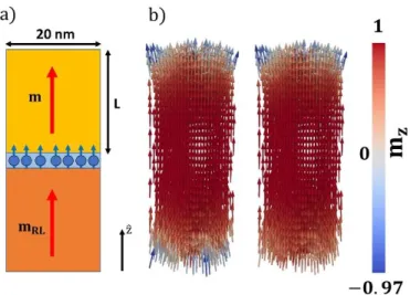
Fig. 1: a) 2D scheme of the studied FeCoB pillars with thickness L and base width of 20 nm. The origin of the iPMA is represented with blue arrows. The storage layer is shown with a yellowish colour, the tunnel barrier with a blue colour and the reference layer with a reddish colour. b) 3D equilibrium initial state of a 60 nm thick FeCoB layer without (left side) and with (right side) iPMA. The colour bar indicates the normalized magnitude of the magnetization along the defined z direction (along the pillar axis) in each cell.
In Fig.1.b) the equilibrium states of a magnetic pillar with and without the effect of the interfacial anisotropy are compared. From Fig.1.b) (left panel) a flower state is observed at both the top and bottom surfaces [28]. However, when considering an iPMA coming from the interface, a sturdier perpendicular orientation of the magnetization is enforced. Thus, the magnetic moments near the bottom surface will follow this preferential alignment, Fig.1.b) (right panel).
On these equilibrium states, a spin-polarized current is injected. In a thin MTJ, this effect is included in the LLGS equation as a damping-like torque term (ΓSTTIP ) and a field-like
torque (the latter neglected in the following simulations) [1]: 𝜕𝑡𝒎 = −|𝛾|𝜇0(𝒎 × 𝐇𝐞𝐟𝐟) + 𝛼(𝒎 × 𝜕𝑡𝒎) + ΓSTTIP , (2)
where 𝛾 is the gyromagnetic ratio, 𝜇0 the vacuum permeability
and:
ΓSTTIP = −|𝛾|𝑎∥𝑉bias𝒎 × (𝒎 × 𝒎𝐑𝐋), (3)
where 𝑎∥ is the pre-factor of the damping-like torque, 𝑉bias the
applied voltage, m the normalized magnetization of the storage layer and mRL the normalized magnetization of the reference
layer.
As the injection of current occurs at the bottom interface, the spin polarization is expected physically to decay exponentially through the interaction with the magnetization [29], [30]. We can model this effect by assuming that the value of 𝑎∥ decreases
spatially:
𝑎∥= 𝑎∥(0) exp {−
𝑧 𝜆STT
}, (4)
where 𝜆STT defines the length scale of the STT decay
throughout the thick layer and 𝑎∥(0) the magnitude at the
interface (origin of the z-axis). In the present work, both 𝜆STT
and 𝜆Ku are assumed to be equal to the height of the elementary
cell. Moreover, the definition of 𝑎∥(0) must be extended to this
micromagnetic representation: 𝑎∥(0) = ℏ 2𝑒 𝜂STT RA 1 𝑀s𝛿FM , (5)
where RA is the resistance-area product of the storage layer, ℏ the reduced Planck constant, e the elementary charge, 𝜂STT the
STT efficiency and 𝛿FM the characteristic magnetic layer
thickness over which the STT is exerted. The latter is 2 nm in this interpretation (due to chosen cell size), as the STT is not affecting the entire magnetic body. In addition, considering the very small area of the pillar, operable PSA-STT-MRAM pillars require a RA product of the order of 1 Ω · 𝜇m2 to avoid
excessive write voltages which may yield dielectric breakdown. The STT efficiency is related to the injected current polarization P. In the case of an inelastic tunnelling in a symmetric junction, the polarization of the first electrode is equal to the polarization of the second electrode:
𝜂STT=
2𝑃 1 + 𝑃2.
(6)
In addition, P is a function of the tunnel magnetoresistance (TMR) [31]-[33]:
𝑃 = √ 𝑇𝑀𝑅
𝑇𝑀𝑅 + 2.
(7)
Assuming that our TMR is higher than 200%, a value of 𝜂STT=
0.94 was chosen. The current pulse is described as a square pulse of 100 ns, with a rising and decay time of 0.1 ns. Further simulations are carried out without considering thermal fluctuations, for a perfectly perpendicular reference layer.
III. MAGNETIZATION REVERSAL DRIVEN BY STT WITHOUT THERMAL FLUCTUATIONS
We consider hereafter different pillar thicknesses (L=30, 40, 50 and 60 nm), and constant width of 20 nm. Figure 2 shows the average magnetization along the symmetry axis for a 𝑉bias
of -1.25 V.
Fig. 2: Time evolution of ⟨𝑚z⟩ for different pillar thicknesses,
𝑉bias= −1.25 V for a pulse length of 100 ns.
For layer thickness of 30 and 40 nm, the switching mechanism exhibits a sharp variation of the magnetization during the short time interval of its reversal. This behavior is different from the one observed for thicker layer, 50 and 60 nm. In those cases, we notice a shoulder during the magnetization reversal, related to a domain wall nucleation and propagation. In all cases there is a slow relaxation in the final decay of ⟨𝑚z⟩,
related with the reversal of the last cell layers. From these data points, it is possible to extract an important feature of the STT-driven reversal, the dependency of the switching time with the applied bias. This switching time (𝜏switch), for a macrospin
regime, defines the time that the magnetization needs during switching to reach an angle close to the z-axis. In micromagnetics, this may be defined as the time needed to switch a certain fraction of the storage layer moment. However, as we have a domain wall propagation, we consider 𝜏switch as
the time it takes to reverse 90% of the magnetic cells, thus preventing cases where the domain wall would switch back the portion already switched of the storage layer. In Fig.3 (left panel) we can see the relation between 𝑉bias and 𝜏switch. The
right panel shows that 𝑉bias is linear with the inverse of 𝜏switch.
This linearity is somehow related to a conservation of the angular momentum during the reversal process, at least in the macrospin regime [34]-[36]. Moreover, as the starting point is the same for the different simulations (within the same L), the slope is related with the magnitude of the perpendicular anisotropy field. For the PSA, this is dominated by the contribution of the shape anisotropy. Thus, by increasing L, this slope gets steeper, as observed. The slowing down of the dynamics is supported by the imposed STT decay, being less efficient to move the domain wall away from the interface.
Fig. 3: Dependency of 𝑉bias on (left panel) 𝜏switch and (right panel) 𝜏switch−1 .
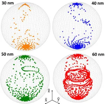
Figure 4 shows the 3D trajectories described by the mean magnetization vector inside the unitary sphere. From these trajectories, an additional confirmation that the underlying mechanism in these structures is not macrospin can be inferred. Even though for 30 and 40 nm this is not straightforward, the magnitude of the average magnetization vector, for each data point, is not unitary. This agrees with a micromagnetic understanding and obvious for 50 and 60 nm, where the switching does not follow the unitary sphere.
Fig. 4: Switching trajectories for layers of different thicknesses. The z-axis represents the ⟨𝑚z⟩ and the basal plane (x and y axis) represents ⟨𝑚x,y⟩. The
simulated data is contained in a macrospin sphere (radius 1). Results obtained for an applied bias of -1.25 V.
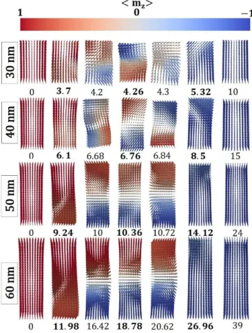
Figure 5 represents 3D magnetization snapshots at different time steps for each thickness. In addition to the switching time (𝜏90% ), two additional characteristic times are shown in bold:
the times at which 10% (𝜏10%) and 50% (𝜏50%) of the magnetic
layer is reversed. Starting with lower thicknesses, as expected, there is no resemblance with a macrospin picture. The
magnetization reversal follows a buckling-like mechanism since the whole magnetic layer reacts during the reversal, the top and bottom edges are coupled strongly by dipolar field [37]-[39].
Fig. 5: Snapshots at different time steps (𝜏10%, 𝜏50% and 𝜏90% in bold) for a
30, 40, 50 and 60 nm thick magnetic layer, for an applied voltage bias of -1.25 V. The color is representative of the magnitude of ⟨𝑚z⟩ and quantified
in the color bar.
Instead, for 50 nm and 60 nm thick pillars, the nucleation of a domain wall starts at the bottom surface. For the frame at 𝜏50%,
two magnetic domains can be observed, in a tail-to-tail domain wall configuration. This domain wall propagates along the symmetry axis of the magnetic layer, while it rotates azimuthally in the transverse plane. This mechanism of reversal is identified as a transverse domain wall propagation [40], [41]. In addition, there is a clear slowing down of the domain wall propagation (supported by the ⟨𝑚𝑧⟩ dependence in Fig. 2)
throughout the pillar when it is at half of its thickness. The sharp slowing down of dynamics upon increasing the height of the pillar is due to the plateau of energy of the domain-wall at mid-height, then only motioned by the exponentially decaying STT arising from the distant interface.
IV. MAGNETIZATION REVERSAL DRIVEN BY STT WITH THE EFFECT OF A THERMAL BATH
Since the magnetization reversal is known to be temperature dependent, thermal fluctuations have been considered to study the impact of the stochasticity. The thermal noise is implemented considering the Brown’s theory [42] by adding an additional random term in 𝐻eff. Therefore, the following
simulations need to be repeated several times to obtain a statistical result.
A study on the evolution of the average magnetization was carried out at a temperature of 300 K considering 100 events and an applied voltage bias between -1 V and -2 V. In fig. 6 (top panel), the temporal evolution of ⟨𝑚z⟩ for an applied
voltage of -1 V, -1.5 V and -2 V is shown. It is observed that for a higher voltage bias, the dispersion in the data points is reduced. It is also obvious that the reversal starts sooner, as the thermal fluctuations drive the magnetization near the bottom surface away from its equilibrium orientation. Therefore, there is a sizable torque experienced by the first layer-cells, which reduces the time needed to nucleate the reversed domain. The time distribution can be further analyzed by considering the statistical dispersion, represented in fig. 6 (bottom panel). The mean values for the different distribution curves were extracted to infer the relation between the switching time and the applied voltage, being displayed in Fig. 7. We further observe that this relation is linear as a function of the inverse of the switching time (as it was the case when no thermal fluctuations were considered). In addition, the reversal mechanism is qualitatively the same, i.e. nucleation of a domain wall followed by its propagation.
Fig. 6: Time evolution of: (top panel) the mean reduced magnetization ⟨𝑚z⟩
at different applied bias. (Bottom panel) distribution of the different processes, associated with each magnetization curves. Histograms enveloped with a lognormal distribution curve. Results obtained for a temperature of 300 K. Values obtained for a pillar thickness of 60 nm and surface width of 20 nm.
V. CONCLUSION
Using micromagnetic calculations, we have investigated the magnetization reversal process in the PSA-STT-MRAM. We considered square pillars of different thicknesses (30, 40, 50 and 60 nm), of 20 nm width. A broad range of applied voltage bias was considered. We have shown that below a threshold thickness of 50 nm, the mechanism of reversal is a collective buckling-like reversal. Above this threshold, a transverse domain wall is nucleated at the bottom surface and propagates along the vertical axis of the pillar. For this regime, a slowing down of the reversal dynamics is observed when the wall is located around the half thickness of the storage layer. That effect gets more pronounced for thicker layers. It was further observed that the inverse of the switching time (τswitch−1 ) follows
a linear relationship with the applied bias voltage (𝑉bias). For
the different thicknesses, the slope of 𝑉bias(τswitch−1 ) grows
steeper as the thickness increases. Moreover, the 𝑉bias(τswitch−1 )
dependence remains linear when considering thermal fluctuations, while retaining the same magnetization reversal dynamics. This study will assist the development of optimized PSA-STT-MRAM cells, providing an understanding behind the switching time and the expected reversal mechanism.
ACKNOWLEDGMENT
At SPINTEC, this study was funded by ERC Advanced Grant MAGICAL No. 669204. At the University of Aveiro, the work was supported by the project i3N, UIDB/50025/2020 & UIDP/50025/2020, financed by national funds through the FCT/MEC.
REFERENCES
[1]. D. Apalkov et al., Proc. IEEE, 104, 1796 (2016)
[2]. A. V. Khvalkovski et al., J. Phys. D: Appl. Phys, 46, 139601 (2013)
[3]. Y. J. Song et al., IEDM Tech. Digest, 18.2.1 (2018) [4]. W. J. Gallagher et al., Symp. VLSI Tech, 190-191 (2019) [5]. S. Ikeda et al., Nature Materials, 9, 721-724 (2010) [6]. B. Cervello et al., Appl. Phys. Lett, 92, 102508 (2008) [7]. Y. J. Song et al., Proc. IEDM, 27.2 (2016)
[8]. Y. K. Lee et al., IEEE Symposium on VLSI Technology, 181-182 (2018)
[9]. Y. C. Shih et al., IEEE Journal of Solid-State Circuits, 54, 231-239 (2019)
[10]. O. Golonzka et al., Proc. IEDM, 18-1 (2018) [11]. J. M. Slaughter et al., Proc. IEDM, 29.3, 85224 (2012) [12]. B. Dieny and M. Chshiev, Rev. Mod. Phys, 89, 025008 (2017). [13]. C. Yoshida et al., Jap. J. Appl. Phys, 58, SBBB05 (2019) [14]. H. Sato et al., Jap. J. Appl. Phys, 56, 0802A6 (2017) [15]. L. Thomas et al., J. Appl. Phys, 115, 172615 (2014 [16]. H. Sato et al., Appl. Phys. Lett., 101, 022414 (2012) [17]. B. Rodmacq et al, US8, 513, 944B2 (2008). [18]. N. Perrissin et al., Nanoscale, 10, 12187 (2018)
[19]. N. Perrisin et al., J. Phys. D: Appl. Phys, 52, 50505 (2019) [20]. S. Lequeux et al., Nanoscale, 12, 6378 (2020)
[21]. K. Watanabe et al., Nature Communications, 9, 663 (2018) [22]. J. Hong et al., Appl. Phys. Lett., 113, 0624 (2018)
[23]. H. Wang et al., IEEE Transactions of Electron Devices, 65, 5537 (2018)
[24]. M. d’Aquino et al., Phys. B: Cond. Matt., 557, 411744 (2020) [25]. B. Dieny et al., Introduction to Magnetic Random-Access
Memory, Wiley-Blackwell, 2017
[26]. L. D. Buda et al., Comput. Mater. Sci., 24, 181 (2002) [27]. N. Strelkov et al., Phys. Rev. B, 95, 184409 (2017) [28]. M. Schabes and H. Bertram, J. Appl. Phys., 64, 1347 (1988) [29]. M. Chshiev, Phys. Rev. B, 92, 104422 (2015)
[30]. J. Grollier et al., Comptes Rendus Physique, 12, 309 (2011) [31]. J. Z. Sun et al., Phys Rev. B., 88, 104426 (2013)
[32]. J. Slonczewski et al., J. Magn. Magn. Mater, 310, 169 (2007) [33]. J. Z. Sun et al., J. Magn. Magn. Mater, 320, 1227 (2008) [34]. K. Garello, Appl. Phys. Lett., 105, 212402 (2014) [35]. H. Liu et al., J. Magn. Magn. Mater., 358, 223 (2014) [36]. D. C. Worledge et al., Appl. Phys. Lett., 98, 022501 (2011) [37]. A. Aharoni, J. Appl. Phys., 63, 4605 (1988)
[38]. A. Aharoni, Phys. Rev, 109, 1522 (1958)
[39]. R. Hertel and J. Kirschner, Physica B, 343, 206 (2004) [40]. R. Hertel, Phys. B: Cond. Matt., 105, 213402 (2014) [41]. A. Thiaville et al., EPL, 69, 990 (2005)
[42]. W. Brown, Phys. Rev., 130, 1677 (1963) Fig. 7: Applied voltage bias as a function of the inverse of the different
characteristic times (1/𝜏𝑒vent). Results obtained for a pillar thickness of 60