HAL Id: hal-02324336
https://hal.archives-ouvertes.fr/hal-02324336
Submitted on 1 Nov 2019
HAL is a multi-disciplinary open access
archive for the deposit and dissemination of
sci-entific research documents, whether they are
pub-lished or not. The documents may come from
teaching and research institutions in France or
abroad, or from public or private research centers.
L’archive ouverte pluridisciplinaire HAL, est
destinée au dépôt et à la diffusion de documents
scientifiques de niveau recherche, publiés ou non,
émanant des établissements d’enseignement et de
recherche français ou étrangers, des laboratoires
publics ou privés.
Characterization of the Electrical Behaviour of Thin
Dielectric Films at Nanoscale using Methods Derived
from Atomic Force Microscopy: Application to Plasma
Deposited AgNPs-Based Nanocomposites
Christina Villeneuve-Faure, K Makasheva, C. Diaou, Laurent Boudou, G.
Teyssedre
To cite this version:
Christina Villeneuve-Faure, K Makasheva, C. Diaou, Laurent Boudou, G. Teyssedre. Characterization
of the Electrical Behaviour of Thin Dielectric Films at Nanoscale using Methods Derived from Atomic
Force Microscopy: Application to Plasma Deposited AgNPs-Based Nanocomposites. 2018 IEEE 13th
Nanotechnology Materials and Devices Conference (NMDC), Oct 2018, Portland, United States.
pp.1-4, �10.1109/NMDC.2018.8605887�. �hal-02324336�
Characterization of the electrical behaviour of thin
dielectric films at nanoscale using methods derived
from Atomic Force Microscopy: application to
plasma deposited AgNPs-based nanocomposites
C. Villeneuve-Faure LAPLACE, Université de Toulouse, CNRS, Toulouse, France villeneuve@laplace.univ-tlse.fr L. Boudou LAPLACE, Université de Toulouse, CNRS, Toulouse, France boudou@laplace.univ-tlse.fr K. Makasheva LAPLACE, Université de Toulouse, CNRS, Toulouse, France makasheva@laplace.univ-tlse.fr G. Teyssedre LAPLACE, Université de Toulouse, CNRS, Toulouse, France teyssedre@laplace.univ-tlse.fr C. Djaou LAPLACE, Université de Toulouse, CNRS, Toulouse, France djaou@laplace.univ-tlse.fr
Abstract— Recent advances in the development of micro- and nano-devices call for applications of thin nanocomposite dielectric films (thickness less than few tens of nanometers) with tuneable electrical properties. For optimization purposes, their behaviour under electrical stress needs to be probed at relevant scale, i.e. nanoscale. To that end electrical modes derived from Atomic Force Microscopy (AFM) appear the best methods due to their nanoscale resolution and non-destructive nature which permits in-situ characterization. The potentialities of electrical modes derived from AFM are presented in this work. The samples under study consist of plasma processed thin dielectric silica layers with embedded silver nanoparticles (AgNPs). Charge injection at local scale, performed by using AFM tip, is investigated by Kelvin Probe Force Microscopy (KPFM). Modulation of the local permittivity induced by the presence of AgNPs is assessed by Electrostatic Force Microscopy (EFM).
Keywords—AFM, KPFM, EFM, nanocomposite dielectrics, plasma processes, SiO2, AgNPs, permittivity
I. INTRODUCTION
Scaling-down the dimensions of micro- and nano-devices requires performant and reliable dielectric layers although their thickness becomes less than 100 nm. An important issue of the insulating parts of devices under electrical stress is the injection and retention of charges that can lead to a breakdown and consequently to a loss of control of the device. For example, the dielectric charging is the main mechanism responsible for the failure and the low reliability of capacitive switches with electrostatic actuation [1], [2]. Control of charge transport in dielectrics is important for many applications: laser printers, electrets, non-volatile memories, solar cells, plasmonic based devices, power electronics, high voltage DC (HVDC) applications, etc., [3]–[5]. Independently on the considered application field, it is actually necessary to implement means for diagnosing the charging state, fitting to the stresses, environment, nature
and geometry of materials and to perform the studies under conditions representative of the real ones. Identification and understanding of the underlying physical phenomena require diagnostic techniques providing information at the scale level where the physical processes occur.
The best suited technique to investigate the dielectric charging phenomenon at nanoscale level is the Atomic Force Microscopy (AFM). Since the AFM was developed, it was used for charge injection in both contact mode [6], [7] and tip-to-sample space mode [8], and for electrostatic lithography [9], [10] of very thin layers. Equally, the AFM was applied for detection of charges by means of its derived electrical modes as Electrostatic Force Microscopy (EFM) [6], [11], [12] or Kelvin Force Microscopy (KFM) [8], [13] and quite recently the Electrostatic Force Distance Curve (EFDC) [14].
The questions still open to debate when dealing with thin dielectric layers, are about the origin of the dielectric charging and the modulation of electrical properties of the dielectric layers. The aim of this work is to present the potentialities of thin nanocomposite dielectric films with tuneable electrical properties and the methodology for their study by using electrical modes derived from AFM.
II. EXPERIMENTS
Aiming at a rational engineering of the electrical properties of thin dielectric layers the studied samples consist of a single layer of silver nanoparticles (AgNPs) embedded in a SiO2 dielectric layer at different distances from the surface.
The nanostructured dielectric layers were deposited on Si substrates in the plasma of an axially-asymmetric radio-frequency (RF) diode discharge sustained at low gas pressure [4], [15]. The discharge powered electrode (smaller electrode) was an Ag-made target to bear the sputtering in order to obtain the AgNPs. The metal sputtering was controlled through the self-bias voltage Vdc, induced on the
powered electrode due to the axially-asymmetric design of that RF discharge. The plasma silica (SiO2) dielectric layers
Research supported by the program IDEX Actions Thématiques Stratégiques – ATS 2015 of the Université de Toulouse under project SEPHIR (2016-066-CIF-D-DRVD).
were obtained in the same reactor with argon-hexamethyldisiloxane (HMDSO, [CH3]6Si2O)-O2 mixture.
A strong originality of this process is the pulsed injection of HMDSO which allows fine tuning of the plasma properties; hence elaboration of high quality plasma silica layers. For both AgNPs and silica layers the thickness was controlled through the deposition time. More details on the reactor, the plasma process, the deposition procedure, and the plasma input parameters are given elsewhere [4], [16]. The structural characterization of the samples was performed by Transmission Electron Microscopy (TEM) in cross-sectional and plan-views, Fourier Transform Infrared (FTIR) spectroscopy and spectroscopic ellipsometry.
AFM measurements were performed on a Bruker MultiMode 8 using Pt-coated Si-tip with resonance frequency f0 of 66.1 kHz, curvature radius Rc of 25nm and a
spring constant k of 2.32 N/m. EFM measurement of the resonance frequency shift Δf0 was done at 20nm-lift with an
applied potential on the tip equal to 0 V or 5 V. Charges were injected using AFM tip in contact mode (contact force of around 30 nN) during 1min at various voltages between -40V and +40V. The resulting surface potential was measured in AM-KPFM mode using a lift of 50nm.
III. ELECTRIC FIELD AND PERMITTIVITY MODELLING
Interpretation of the obtained results through KPFM and EFM measurements was achieved after computing the electric field and electric force for the experimental dielectric structures by using a 2D-axisymmetric Finite Element Model (FEM) on COMSOL platform. Classical approximation was used to describe the AFM tip, with the later consisting in a truncated cone of 10 μm height and 14° aperture angle, ending by a semi-spherical apex (curvature radius Rc) [17]. The tip was surrounded by an air box with
large enough dimensions to avoid edge effects. The relative dielectric permittivity of SiO2 and Si were taken equal to 3.9
and 11.4 respectively.
For correspondence to the experimental arrangement the potential was applied on the tip and the silicon substrate back side was grounded. No charge conditions (zero potential) were applied as boundary conditions on the free boundaries of the simulation box.
The electric field E was computed in air and in the dielectric matrix using Poisson’s equation. The electrostatic force Fe was obtained after integration of the electric field E
over the AFM tip surface according to the equation [18]: 2 0 . .ds 2 e F E
n (1)where 0 is the dielectric permittivity.
IV. RESULTS AND INTERPRETATION
A. Nanostructured dielectric layers characteristics
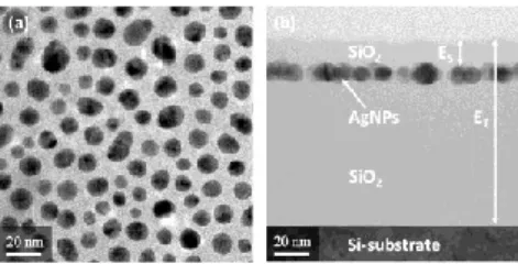
A view of the general structure of the nanostructured thin dielectric layers containing AgNPs is presented in Fig. 1. The AgNPs are not percolated and uniformly distributed (Fig.1a), organized in a single layer (Fig. 1b). Their shape is rather prolate spheroid with randomly oriented major axis. The main characteristics of the studied samples are summarized in Table I: total thickness (ET), major axis of
the AgNPs and thickness of the SiO2 cover layer (ES).
The AgNPs are exposed on the surface of a SiO2 layer or
embedded at different distances from the SiO2 surface. Two
sizes of AgNPs are considered. The SiO2 cover layer is
conformal to the shape of AgNPs imposing slight waviness of the surface for the thinner cover layers (5.0 and 7.0 nm).
TABLE I. SAMPLE DESCRIPTION: SAMPLE TOTAL THICKNESS (ET), AGNPS MAJOR AXIS (D) AND SIO2 COVER LAYER THICKNESS (ES)
ET (nm) D (nm) ES (nm) 1 150.61.8 - - 2 80.01.0 11.02.4 - 3 97.03.4 11.02.4 5.01.5 4 203.09.6 19.67.8 7.01.8 5 193.08.4 19.67.8 21.02.0 B. Charges injection
First of all, charge injection in thin nanostructured layers was studied. Fig. 2 shows the surface potential profiles modified by injected charge recorded on the three types of structures: SiO2 layer alone and SiO2 layer with AgNPs
embedded at different positions in the volume. From this typical bell-like shape profile two relevant parameters are extracted : (i) the Full Width at Half Maximum (FWHM) which reflects charge lateral spreading and (ii) the area under the potential profile (labelled IS) which represents in
first approximation (dielectric layers within the same thicknesses range) the amount of injected charges [19].
Nanoparticles influence on injected charge is already emphasized on Fig. 2. Indeed, smaller charge amount seems to be injected in nanocomposite layer with AgNPs far from surface whereas quite the same behavior is observed for no AgNPs or nanoparticles embedded close to the surface.
Fig. 3a shows the evolution of potential profile FWHM as a function of the lateral electric field applied during charge injection. The FWHM increases with the electric field for both polarities, and for all samples. So electrons and holes exhibit quite the same spreading dynamics regardless the nanoparticle position in the dielectric layer.
As to the charge spreading, Fig. 3b shows that the area under the peak increases with the electric field at the injection point. This implies that the amount of injected charges increases with the electric field in the same way for electrons and holes. Moreover, the amount of injected charges seems a little bit higher when the AgNPs are closer to the surface. One of the hypothesis to explain this already observed phenomenon [4], is that the AgNPs act as traps for the injected charges. But in this configuration, the contribution of this phenomenon seems to be weaker than the electric field enhancement due to the presence of nanoparticles. To emphasize this possibility, effective dielectric permittivity of the structure needs to be probed at nanoscale.
Fig. 1. (a) Brigth field plan-view TEM image and (b) bright field cross-section TEM image of the general structure of nanostructured thin dielectric layers under study.
C. Influence of nanoparticules on permittivity
In this part the effective permittivity map is extracted from the frequency shift measured by EFM using a method derived that of C. Riedel et al. [12]. EFM provides in the same time surface topography and resonance frequency shift Δf0 (Vi) for a voltage Vi applied to the tip. In this study, the
frequency shift is probed at 0V and 5V, and the resulting frequency shift parameter aΔf is determined using the
following equation:
aΔf = [Δf0 (5V)- Δf0 (0V)]/(5)². (2)
From a theoretical point of view this parameter is related to capacitance C by:
aΔf = f0 /(4k) d²C/dz², (3)
where z is the vertical distance and k is the stiffness of the cantilever. The quantity d²C/dz² is determined using the electrostatic force Fe computed at different lift positions and
different permittivities using the FEM model, leading to a theoretical relation between εr and aΔf. In a first
approximation, this relation was computed for a homogeneous dielectric matrix with different relative permittivities in the range from 1 to 10. Using this, the plasma deposited SiO2 samples alone exhibit a relative
permittivity of 3.7 which is close to the dielectric permittivity of stoichiometric SiO2.
Fig. 4a presents the obtained results for SiO2 layers with
AgNPs exposed on the surface (Figs. 4a-c) and with AgNPs embedded at 5nm under the surface (Figs. 4d-f). Fig. 4a shows that the AgNPs exposed on the surface of SiO2 are
visible on the topography map. Following the methodology described above, the obtained frequency shift parameter aΔf
(Fig. 4b) permits to determine the permittivity map (Fig. 4c). The results emphasize that the permittivity is lower on the AgNPs and increases in-between the AgNPs imposing an average value of around 4.4 which is higher than the one for SiO2 alone. When the AgNPs are embedded at 5nm
beneath the surface their influence is less visible either on topography (Fig. 4d), frequency shift parameter (Fig. 4e) and permittivity (Fig. 4f) maps. Indeed, the contrast between the permittivity above and between AgNPs is lower and its mean value around 4.2 is closer to that of matrix (Fig. 4f).
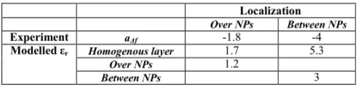
Computing the electric field is needed to understand the above described effect. Fig. 5 compares the electric field distribution in different configurations and highlights that the presence of AgNPs close to the surface enhances the electric field. This effect is further amplified if the AFM tip is localized on the nanoparticles compared to a position between them. The theoretical relation between εr and aΔf
was computed for each of these configurations. Table II summarizes the effective dielectric permittivity deduced
Fig. 2. Surface potential measured by AM-KPFM after charge injection at -40V during 1min in SiO2 with and without AgNPs. 0 5 10 -1.5 0.0 Sur face po te nt ial p ro file ( V ) Lateral position (µm) No AgNPs AgNPs with D=19.6nm Es=7nm Es=21nm
Fig. 3. Evolution of (a) the surface potential profile FWHM as a function of lateral electric field during charge injection, (b) the area under the potential profile as a function of maximum electric field. SiO2 layer with and without embedeed AgNPs.
-1.5 -1.0 -0.5 0.0 0.5 1.0 1.5 0 1 2 No AgNPs AgNP with D=19.6nm Es=7nm Es=21nm FWH M (µm)
Lateral electric field (109 V/m) (a) -6 -4 -2 0 2 4 6 -8 -4 0 4 8 No AgNPs AgNPs with D=19.6nm Es= 7nm Es=21nm Are a I S ( V µm )
Electric field at injection point (109 V/m) (b)
Fig. 4. (a-c) 80nm-thick SiO2 layer with AgNPs on the surface, (d-f) AgNPs embedded at 5nm under the surface. (a, d) Surface topography, (b, e) frequency shift parameter aΔf and (c,f) relative permittivity.
Fig. 5. Electric field computed by FEM: (a) SiO2 layer alone, (b) over the AgNPs and (c) between the AgNPs exposed on SiO2 layer, with 20nm-lift and 5V applied on the tip.
from the experimental results after employing the appropriate model. Now, the permittivity above the AgNPs appears close to 1 which actually corresponds to the dielectric permittivity of air. The AgNPs screen completely the material contribution under them. The permittivity between nanoparticles appears to be around 3, a value close to the dielectric permittivity of the matrix. This lower value is probably due to capacitive contribution of neighboring nanoparticles. The same phenomenon is observed for AgNPs embedded at 5nm from the surface. Indeed, taking into account the real geometry, the obtained relative permittivity is around 2.7 and 4, on the AgNPs and between the nanoparticles, respectively.
TABLE II. COMPARISION OF THE RELATIVE PERMITTIVITY DETERMINED BY DIFFERENT MODEL CONFIGURATIONS TAKING INTO ACOUNT THE SAMPLE GEOMETRY
Localization
Over NPs Between NPs
Experiment aΔf -1.8 -4
Modelled εr Homogenous layer 1.7 5.3
Over NPs 1.2
Between NPs 3
The same effect is observed for AgNPs embedded at 7nm from the surface over a thicker SiO2 layer (Figs. 6a and
6b). When the nanoparticles are embedded far from the surface (Figs. 6c and 6d), their contribution to the effective dielectric permittivity becomes negligible as the contrast due to nanoparticles decreases and the determined effective dielectric permittivity is close to 3.8, which is actually close to the dielectric permittivity of the matrix.
This observed screening effect in presence of AgNPs is due to their metallic nature. Indeed, computational results show that dielectric nanoparticles with permittivity of 80 (TiO2) or 7.5 (SiNx) influence slightly the electric field
distribution, even if they are situated close to the layer surface. No modification on the theoretical relation between εr and aΔf is observed.
V. CONCLUSION
Results from KPFM and EFM measurements on plasma deposited AgNP-based nanostructured dielectric layers show that when the AgNPs are embedded in the SiO2
plasma deposited dielectric layer they completely screen the influence of the dielectric matrix under them. This results in lower effective relative permittivity when the metallic nanoparticles are embedded close to the dielectric surface (less than 7nm under). Moreover, the presence of AgNPs induces electric field enhancement which increases the amount of injected charges for a fixed applied bias (i.e. for the macroscopic electric field). Further investigations are needed to determine the influences of AgNPs on the charge localization in the volume.
The results obtained in this work emphasize that electrical modes derived from AFM are powerful tools to characterize the electrical properties of thin dielectric layers either for homogeneous or nanostructured (with embedded AgNPs) ones. However, the real sample geometry should be taken into account in the interpretation of the recorded experimental results.
REFERENCES
[1] A. Witvrouw, H. A. C. Tilmans, and I. De Wolf, “Materials issues in the processing, the operation and the reliability of MEMS,” Microelectron. Eng., vol. 76, no. 1–4, pp. 245–257, Oct. 2004. [2] J. Iannacci, “Reliability of MEMS: A perspective on failure
mechanisms, improvement solutions and best practices at development level,” Displays, vol. 37, pp. 62–71, Apr. 2015.
[3] C. A. Rezende, R. F. Gouveia, M. A. da Silva, and F. Galembeck, “Detection of charge distributions in insulator surfaces,” J. Phys. Condens. Matter, vol. 21, no. 26, p. 263002, Jul. 2009.
[4] K. Makasheva et al., “Dielectric Engineering of Nanostructured Layers to Control the Transport of Injected Charges in Thin Dielectrics,” IEEE Trans. Nanotechnol., vol. 15, no. 6, pp. 839–848, Nov. 2016.
[5] L. Milliere, K. Makasheva, C. Laurent, B. Despax, and G. Teyssedre, “Efficient barrier for charge injection in polyethylene by silver nanoparticles/plasma polymer stack,” Appl. Phys. Lett., vol. 105, no. 12, p. 122908, Sep. 2014.
[6] B. D. Terris, J. E. Stern, D. Rugar, and H. J. Mamin, “Contact electrification using force microscopy,” Phys. Rev. Lett., vol. 63, no. 24, pp. 2669–2672, Dec. 1989.
[7] S.-D. Tzeng, K.-J. Lin, J.-C. Hu, L.-J. Chen, and S. Gwo, “Templated Self-Assembly of Colloidal Nanoparticles Controlled by Electrostatic Nanopatterning on a Si3N4/SiO2/Si Electret,” Adv. Mater., vol. 18, no. 9, pp. 1147–1151, May 2006.
[8] L. Ressier and V. Le Nader, “Electrostatic nanopatterning of PMMA by AFM charge writing for directed nano-assembly,” Nanotechnology, vol. 19, no. 13, p. 135301, Apr. 2008.
[9] E. D. Herbschleb et al., “Direct imaging of coherent quantum transport in graphene p−n−p junctions,” Phys. Rev. B, vol. 92, no. 12, Sep. 2015. [10] P. Marconcini and M. Macucci, “Numerical analysis of the resistance behavior of an electrostatically-induced graphene double junction,” J. Comput. Electron., vol. 14, no. 3, pp. 653–660, Sep. 2015.
[11] M. A. Reagan, D. Kashyn, S. Juhl, R. A. Vaia, and S. F. Lyuksyutov, “Electric charging and nanostructure formation in polymeric films using combined amplitude-modulated atomic force microscopy-assisted electrostatic nanolithography and electric force microscopy,” Appl. Phys. Lett., vol. 93, no. 3, p. 033109, Jul. 2008.
[12] C. Riedel et al., “Determination of the nanoscale dielectric constant by means of a double pass method using electrostatic force microscopy,” J. Appl. Phys., vol. 106, no. 2, p. 024315, Jul. 2009.
[13] C. Villeneuve-Faure et al., “Kelvin force microscopy characterization of charging effect in thin a-SiOxNy:H layers deposited in pulsed plasma enhanced chemical vapor deposition process by tuning the Silicon-environment,” J. Appl. Phys., vol. 113, no. 20, p. 204102, May 2013. [14] C. Villeneuve-Faure, L. Boudou, K. Makasheva, and G. Teyssedre,
“Atomic force microscopy developments for probing space charge at sub-micrometer scale in thin dielectric films,” IEEE Trans. Dielectr. Electr. Insul., vol. 23, no. 2, pp. 713–720, Apr. 2016.
[15] B. Despax and P. Raynaud, “Deposition of ‘Polysiloxane’ Thin Films Containing Silver Particles by an RF Asymmetrical Discharge,” Plasma Process. Polym., vol. 4, no. 2, pp. 127–134, Feb. 2007. [16] A. Pugliara, C. Bonafos, R. Carles, B. Despax, and K. Makasheva,
“Controlled elaboration of large-area plasmonic substrates by plasma process,” Mater. Res. Express, vol. 2, no. 6, p. 065005, Jun. 2015. [17] C. Villeneuve-Faure, K. Makasheva, L. Boudou, and G. Teyssedre,
“Charge injection in thin dielectric layers by atomic force microscopy: influence of geometry and material work function of the AFM tip on the injection process,” Nanotechnology, vol. 27, no. 24, p. 245702, Jun. 2016.
[18] J. Colchero, A. Gil, and A. M. Baró, “Resolution enhancement and improved data interpretation in electrostatic force microscopy,” Phys. Rev. B, vol. 64, no. 24, Nov. 2001.
[19] C. Villeneuve-Faure, L. Boudou, K. Makasheva, and G. Teyssedre, “Methodology for extraction of space charge density profiles at nanoscale from Kelvin probe force microscopy measurements,” Nanotechnology, vol. 28, no. 50, p. 505701, Dec. 2017.
Fig. 6. (a,c) Surface topography and (b, d) the relative permittivity of a 200nm-thick SiO2 sample with AgNP emdedded (a-b) at 7nm and (c-d) at 21nm under the surface.