HAL Id: hal-01820721
https://hal.archives-ouvertes.fr/hal-01820721
Submitted on 22 Jun 2018
HAL is a multi-disciplinary open access
archive for the deposit and dissemination of
sci-entific research documents, whether they are
pub-lished or not. The documents may come from
teaching and research institutions in France or
abroad, or from public or private research centers.
L’archive ouverte pluridisciplinaire HAL, est
destinée au dépôt et à la diffusion de documents
scientifiques de niveau recherche, publiés ou non,
émanant des établissements d’enseignement et de
recherche français ou étrangers, des laboratoires
publics ou privés.
Curved detectors developments and characterization:
application to astronomical instruments
Simona Lombardo, Thibault Behaghel, Bertrand Chambion, Wilfried Jahn,
Emmanuel Hugot, Eduard Muslimov, Melanie Roulet, Marc Ferrari,
Christophe Gaschet, Stéphane Caplet, et al.
To cite this version:
Simona Lombardo, Thibault Behaghel, Bertrand Chambion, Wilfried Jahn, Emmanuel Hugot,
et al..
Curved detectors developments and characterization: application to astronomical
instru-ments. SPIE Astronomical Telescopes and Instrumentation, Jun 2018, Austin, TX, United States.
�10.1117/12.2312654�. �hal-01820721�
Curved detectors developments and characterization:
application to astronomical instruments
Simona Lombardo
a, Thibault Behaghel
a, Bertrand Chambion
c, Wilfried Jahn
b, Emmanuel
Hugot
a, Eduard Muslimov
a, Melanie Roulet
a, Marc Ferrari
a, Christophe Gaschet
c,
St´
ephane Caplet
c, David Henry
ca
Aix Marseille Univ, CNRS, CNES, LAM, Marseille, France;
bDivision of aerospace engineering, Caltech, Pasadena, CA 91125, USA;
cUniv. Grenoble Alpes, CEA, LETI, MINATEC campus, F38054 Grenoble, France
ABSTRACT
Many astronomical optical systems have the disadvantage of generating curved focal planes requiring flattening optical elements to project the corrected image on flat detectors. The use of these designs in combination with a classical flat sensor implies an overall degradation of throughput and system performances to obtain the proper corrected image. With the recent development of curved sensor this can be avoided. This new technology has been gathering more and more attention from a very broad community, as the potential applications are multiple: from low-cost commercial to high impact scientific systems, to mass-market and on board cameras, defense and security, and astronomical community.
We describe here the first concave curved CMOS detector developed within a collaboration between CNRS-LAM and CEA-LETI. This fully-functional detector 20 Mpix (CMOSIS CMV20000) has been curved down to a radius of Rc=150 mm over a size of 24x32 mm2. We present here the methodology adopted for its characterization
and describe in detail all the results obtained. We also discuss the main components of noise, such as the readout noise, the fixed pattern noise and the dark current. Finally we provide a comparison with the flat version of the same sensor in order to establish the impact of the curving process on the main characteristics of the sensor. Keywords: CMOS, curved detector, characterization, noise properties, dark current
1. INTRODUCTION
Many astronomical optical systems have the disadvantage of generating curved focal planes requiring flattening optical elements to project the corrected image on flat detectors. The use of these designs in combination with a classical flat sensor implies an overall degradation of throughput and system performances to obtain the proper corrected image. This is extremely harmful in case the science goal requires an instrumental PSF as compact as possible e.g. to measure the ultra-low surface brightness universe. One example for this is the space mission MESSIER which aims at measuring surface brightness levels as low as 35 mag arcsec−2 in the optical (350-1000 nm) and 38 mag arcsec−2 in the UV (200 nm). Any refractive surface must also be excluded in this design as they would generate Cherenkov emission due to the relativistic particles. This automatically eliminates the possibility of using optics to flatten curved focal plane.
With the recent development of curved detectors,1–5 this is not an issue anymore. The introduction of
curved detectors has two additional advantages: it allows to have a reduction of the size of the imaging systems, consequently making their design more compact and simpler (particularly important for space missions), and, at the same time, it improves their overall performances (e.g. higher resolution). This new technology has been gathering more and more attention from a very broad community, as the potential applications are multiple: from low-cost commercial to high impact scientific systems, to mass-market and on board cameras,defense and security,6 and astronomical community.
A version of MESSIER with reduced dimensions is planned as its ground-based demonstrator.7 This fully
reflective Schmidt design will be installed in Tenerife and it will potentially be the first astronomical telescope [email protected]
that uses a curved detector – with convex shape and a radius of curvature of 800 mm – probing the full capabilities of this groundbreaking technology.
In this paper, we describe the first concave curved CMOS detector developed within a collaboration between CNRS-LAM and CEA-LETI. This fully-functional detector of 20 Mpix (CMOSIS, CMV200008) has been curved down to a radius of 150 mm over a size of 24x32 mm2 and it is sensitive to the visible light. Specific care was taken to keep the packaging identical to the original one before curving, in such a way that the final product is a plug-and-play commercial component.
We present here the methodology adopted for its characterization (Section3) and describe in detail all the results obtained (Section4). We also discuss the main components of noise, such as the readout noise, the fixed pattern noise and the dark current. Finally we provide a comparison with the flat version of the same sensor in order to establish the impact of the curving process on the main characteristics of the sensor.
2. CURVING PROCESS
CEA-LETI in collaboration with CNRS-LAM is in a phase of prototyping several curved detectors concepts. Such detectors have already shown promising results and demonstrated some of the improvements achievable in term of compactness and performances of the related optical designs.9
The off-the-shelf initial flat sensor consists of a silicon die glued on a ceramic package. Wire bonding from the die to the package surface provides the electrical connections. Finally a glass window protects the sensor surface from mechanical or environment solicitations (figure 1A). The curving process of these sensors consists of two steps: firstly the sensors are thinned with a grinding equipment to increase their mechanical flexibility, then they are glued onto a curved substrate. The required shape of the CMOS is, hence, due to the shape of the substrate. The sensors are then wire bonded keeping the packaging identical to the original one before curving. The final product is, therefore, a plug-and-play commercial component ready to be used or tested (figure 1B).
i i i i i sum n n r n n Petzval 1 1 (1)
Where n is the refractive index of the incident and refractive medium, r is the radius of curvature of the considered diopter. Usually, the correction of this aberration is done by the use of divergent elements called “field flatteners”, discovered by Charles Piazzi Smyth in 1875 [1], which minimize drastically the Petzval sum to coincide with a flat sensor. The second interest was the discovery made by Thomas Sutton in 1860, with the monocentric system, or concentric system [2]. In this system, all optical surfaces are spherical and share the same center of curvature, and with this symmetry, multiple aberrations as the coma and astigmatism are cancelled out. This is an aberration free design and will be our optical design starting point (section 3). And the third technology with an interest for sensor’s curvature was the Schmidt telescope which provide wide field of view, limited aberrations with a curved detector [4]. For all these discoveries, the use of curved sensors was possible but limited. In fact, the solid photographic plate used in the 19th centuries was too delicate for a commercial purpose. And with the patent of Hannibal Goodwin in 1887 [3], flexible photographic films have been used. Since the launch of silicon industry, image sensors has been limited to flat and rigid. But some recent developments show a new interest for curved sensors. Firstly, there are several developments on the fabrication of curved sensors. For the monolithic approach, the fabrication has been demonstrated on uncooled and cooled infrared sensors, for very compact high-performance camera [5], Charge Couple Device (CCD) [6], or Complementary Metal Oxide Semiconductor (CMOS) [7, 8]. None are in industrial production. Secondly, there are also some developments on optical improvements of optical systems with curved sensors, on optical advantages, for instance on camera-phone [9], or astronomical applications [10], and also on the simplification of optical systems by reducing weight, volume or number of lenses [11]. A study on telescope combining free-form optics and curved detectors showed also a better field of view and f number [12].
2.2 Curved packaging and process
This work is based on the commercial product 1/1.8’’ format 1.3Mpx global shutter CMOS sensor (Teledyne EV76C560) [13]. The standard sensor structure basically consists of a silicon die (7.74 x 8.12 mm), glued on a ceramic package. Electrical connections are wire bonded from the die to the package surface and then, to the interconnection board thanks to a reflow process. On top, a glass cover is placed to prevent from mechanical or environment solicitations. This structure is shown in figure 1.
Figure 1: a) Commercial Teledyne EV76C560 flat sensor. b) Associated schematic view along A-A’ axis. In order to implement a spherically shaped CMOS sensor, changes are required to adapt this standard structure. First, the sensor is thinned with a grinding equipment to a targeted thickness in order to make the sensor mechanically “flexible”. It can be followed by a Chemical Mechanical Polishing (CMP). In this work the targeted thickness is 100µm. The bendable capabilities of the CMOS sensor will be detailed in section 2.4. Then, that thinned chip is glued (structural attachment) onto a curved substrate. The CMOS final shape is drove by the substrate. Wire bonding process, developed for electrical connections, is also optimized in order to prevent damages on thinned dies. Figure 2 shows a schematic of the final packaging, curved into its commercial packaging. The radius of curvature is R=65mm.
Figure 2: a) Curved Teledyne EV76C560 sensor (R=65mm). b) Associated schematic view along B-B’’ axis. 2.3 Associated mechanical modeling
Mechanical considerations of the curved sensors are an important part to develop optical system design and find curving limitation for the sensor. For an analytical analysis, the shell theory has been used to model the mechanical behavior of the semiconductor die. This analytical model is presented in [14]. The mechanical behavior has been also modeled, using ANSYS ® Finite Element Analysis (FEA) software. For this study, extensive simulation were conducted on 7.74 x 8.12 mm (100)-oriented silicon chip with specific quadrangle elements are used, defined by 4 nodes, 6 degrees of freedom each (SHELL 181 elements). Using these elements, the principle stress values on the bottom, middle and top surfaces of the plate are obtained. Based on a breakage ball on ring study and curved packaging work [8,15] on silicon square plates with different grinding, polishing, and sawing processes, two tensile failure strength criterions has been defined: S1max1 = 200MPa, which refers to a standard grinding and sawing, and S1max2= 500MPa, associated to CMP
process and standard sawing.
The parameters are the thickness t of the plate with a range value from 25 to 125 µm and its radius of curvature. The die was discretized into approximately 5000 elements. For silicon mechanical data, the following reduced stiffness coefficient matrix is used, with only three independent elastic coefficients:
44 44 44 11 12 12 12 11 12 12 12 11 100 c c c c c c c c c c c c C (2)
where c11 = 165.7GPa, c12 = 63.9GPa, c44 = 79.6 GPa [16]. The minimum allowable radius of curvature are extracted
from the FEA results for both tensile failure strength criterions. Results of the minimum allowable radius of curvature are plotted on figure 3.
With this two failure criterions methodology, three areas are defined: the safe area without any breakage risk with a standard grinding and sawing (S1< S1max1), a forbidden area where the intrinsic silicon mechanical limits are over (S1>
S1max2), and a in between zone for processes optimizations. With our targeted thickness of 100 µm, and considering our
thinning process, we expect a minimum allowable radius of curvature Rc min=32 mm before silicon breakage.
Removable glass cover
A
B
Figure 1. Schematic view of the commercial flat CMOS (A) and curved (B). From.9
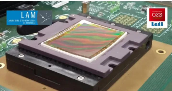
In this paper we show the electro-optical characterization results of one of our prototype. This chip (Figure2) is a CMV20000 global shutter CMOS image sensor from CMOSIS, with 5120×3840 pixels of 6.4 µm size. It has been curved with a spherical concave shape down to a radius of 150 mm.
3. CHARACTERIZATION METHODOLOGY OF CURVED CMOS
In order to know how the curving process impacts the noise properties and the performances of the detector itself, a set of characterization measurements is performed on the curved detector and on its equivalent flat version and their results are compared. Typical measured quantities are:10,11 detector gain, dark current, readout noise,
fixed pattern noise, dynamic range and full well capacity.
The dark current is due to the thermal agitation of the electrons within the semiconductor and it is extremely sensitive to the temperature. This agitation can free the electrons which are, hence, collected in the potential wells of the pixels, becoming indistinguishable from the charges due to a direct illumination. It is usually obtained by reading out the detector at different exposure times in complete darkness conditions. As the averaged signal linearly grows as function of exposure time, the dark current is estimated by fitting these measurements.
Figure 2. CMV200008 CMOS image sensor from CMOSIS plugged on the CMOSIS evaluation board. This sensor has
been curved with a spherical concave shape down to a radius of 150 mm.
The value of the gain (which determines how the amount of charge collected in each pixel will be assigned to a digital number in the image) is instead obtain by exposing the detector to uniform and constant illumination, at different exposure times. Again the average signal, registered on the detector at each exposure time, grows linearly as function of exposure time until it reaches saturation. More details regarding the methodologies adopted to measure all the mentioned characterization values are provided in the following subsections.
3.1 Data acquisition
The following measurements were performed:
• For each exposure time, 30 frames were acquired.
• Firstly exposures to uniform light – also called flat fields – have been performed, and then exposures in complete darkness.
• The exposure time has been changed with values ranging from 0.0002 s to saturation, for flat field exposures, and to 0.96 s for the dark exposures.
• The concave (Rc=150 mm) and a flat CMOS have been tested using the same set of measurements.
• The measurements were performed with camera gain set to 1.
The communication between sensor and computer was made through the CMV20000 evaluation kit. In order to achieve a uniform illumination of the sensors, we used an integrating sphere and placed it at 1.07 m distance from the sensor. The entrance port of the sphere was illuminated by a tungsten bulb placed inside another smaller integrating sphere. A series of light baffles were located all around the light path to reduce the scattered light. In order to avoid systematics due to the drifting of the light level or small (< 0.1oC) temperature fluctuations the exposure time was sampled almost randomly, by alternating measurement sets with shorter and longer exposure time.
The measurements were performed at a room temperature of 21.9±0.1oC for the concave sensor and 21.0±0.1oC for the flat one. The CMOS temperature was monitored by the internal temperature sensor (calibrated for each sensor with thermocouples) and, during the full characterization, resulted to be 35.1±0.2oC for the concave sam-ple and 34.9 ± 0.2oC for the flat sensor (the errors represent a variation of temperature during the measurements and not the error on the absolute value).
3.1.1 Methodology used for dark current and readout noise measurements
After acquiring the measurements, a series of data processing was required to obtain the desired characterization values. As previously mentioned for each exposure time a set of 30 dark exposure frames was acquired and a median image was obtained. By averaging further over the pixels, a mean signal level was obtained. By fitting
the linear trend of the average signal as function of exposure time one obtains the dark current and the bias level (which is a positive offset set up by the electronics to avoid recording negative numbers).
An important noise component is the temporal noise, which is the variation in time of the output value of the pixels exposed to a constant illumination. It is typically composed of the shot noise, due to the dark current or light exposure, and of the noise generated when reading out the pixels (readout noise, RON). The temporal noise is obtained by computing the standard deviation of each pixel in the 30 frames acquired for each exposure time: an image is created, where each pixel is a standard deviation of the mean value of the pixel in the 30 frames. The temporal noise (for a specific exposure time) is, hence, the mean of these standard deviations.
From the temporal noise of the shortest exposure time dataset acquired in complete darkness, we measured the RON.
3.1.2 Methodology used for gain and PRNU measurements
The gain and the pixel response non-uniformity (PRNU) are measured from flat field images. As before 30 frames were acquired for each exposure time (sampling the exposure time randomly). From these, a median image was obtained for each exposure time. Then an average over all pixels was computed, thus providing a mean signal level. The exposure times were sampled alternating short and long ones (as before) and they ranged between 2.4×10⁻⁴s and 0.48 s, to allow the sensor to reach saturation.
Additionally, we estimated the temporal noise as in Section3.1.1, but this time using the flat field exposures. The square of the temporal noise, σtemp, can be written as:10
σ2temp= const + k(Smean− Soffset), (1)
where k is the gain in units of DN/e− and Smean− Soffsetare the mean signal on the median image and the bias
level (computed from the dark exposures) respectively. Equation1 shows the linear relation between the mean signal and the temporal noise, which leads to the estimation of the gain, k, by making acquisitions at different the exposure times.
Typically the noise of an image contains also the PRNU. This is due to slightly different responses to incoming light, among the pixels of a sensor, and it is directly proportional to the number of electrons detected through the PRNU factor, fPRNU. The total noise of an image can be written as:11
σtot= q σ2 e + σ2RON+ σ 2 PRNU (2)
where σe is the shot noise, σRON is the readout noise, and σPRNU is the PRNU noise. As the PRNU does not
depend on time, by subtracting one frame to another with equal exposure time, we eliminated its contribution from the noise equation, and we were able to estimate the shot noise. From Equation2we obtained σPRNUand
estimated fPRNU, which is usually expressed as a percentage of the mean signal.
4. RESULTS
In Section3we described the acquisition methodology and the data processing applied to obtain the fundamental values for characterizing the sensors. In this Section we show the results obtained from the different datasets for the concave and flat samples.
Following the prescription in Section 3.1.1, we obtained the results in Figure 3. The linear increase of measured signal for exposure times larger than 0.048 s is due to the accumulation of charges caused by the dark current. By fitting these data we estimated the dark current in DN/s (the slope of the fit) and the bias level (the intercept of the fit). We obtained for the dark current a value of 80.68±0.70 DN/s for the concave sample (at 35.1oC) and of 94.90±0.59 DN/s for the flat sensor (at 34.9oC). The errors here are the 1σ errors on the linear
fit.
For the shorter exposure times, the counts on the sensor increase and the response is not linear. As this feature is present in both sensors, we concluded that it is an intrinsic characteristic of the CMV20000. We applied the
Exposure time (s) Exposure time (s) Me a n D a rk Si g n a l (D N ) Me a n D a rk Si g n a l (D N )
Flat
Concave
Figure 3. Mean dark exposure signal as function of exposure time. The black line is the fit to the data for exposure time larger than 0.048 s. Left: data for the flat sensor. Right: data for the concave sensor.
definition of bias level – the mean value of the median frame with the shortest exposure time acquired in darkness – and therefore we used this higher value, specified in Table1, as bias level in the following.
The dark exposures also allowed us to estimate the readout noise from the temporal noise of the dataset with the shortest exposure time, as explained in Section3.1.1. The values obtained are in Table1. In order to asses if the dark current and readout noises present any significant difference among the two sensors, we first evaluated their gain. Only after converting the DN in number of electrons we can have a fair comparison.
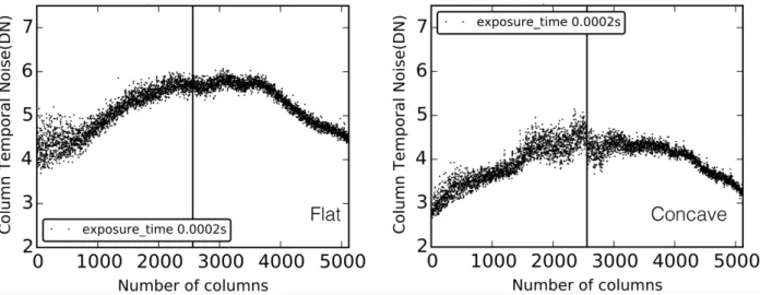
Before measuring the gain, another useful diagnostic way to evaluate the performances of CMOS sensors is the column temporal noise. This is done by plotting the standard deviation of each sensor column in the median image (from the 30 images acquired) of the dark exposure with the shortest exposure time (in this case). The column temporal noise as function of column number is shown in Figure4 and does not present any particular difference between the two sensors. We notice a slightly larger scatter of the values for the concave sample but such values show a similar behaviour compared to the flat sensor case – they increase at the center and decrease at the two edges – and they are also overall smaller.
Figure 4. Column temporal noise of a median dark exposure image at 0.0002 s vs column number for the flat (left) and the concave (right) sensors.
The gain was measured as explained in Section3.1.2, from a set of flat fields where the sensor is exposed to uniform and stable illumination. In Figure5 the mean signals observed by the two sensors are shown vs the exposure times. The signal grows linearly for exposure times larger than 0.048 s until it reaches the saturation limit of 4095 DN (set by the Analog Digital Converter, as it has 12-bit per pixel) for both sensors. From this we estimated the full well capacity by subtracting the bias level to the saturation limit, and the dynamic range as DR = 20log(Smax/RON) where Smaxis the saturation limit and RON is the readout noise. These values are
shown in Table1.
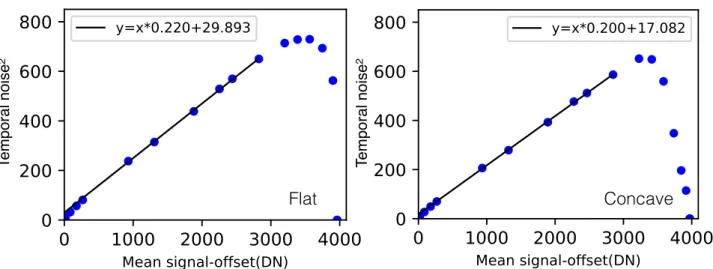
In Figure 6 are plotted the squared temporal noises of both detectors against the mean signal - offset. For values of mean signal - offset between 1000 DN and 3000 DN we see a linear trend as the one described by Equation 1. From the slope of the fit to the linear part, we obtained a gain of 0.200±0.002 DN/e− and
0.220±0.003 DN/e− for the concave and flat sensors respectively (again, the errors are the 1σ errors on the linear fit). This two values are apart by 10%, however we cannot conclude that this difference is due to the curving process as it might be within the manufacturing scatter. The gain quoted by the manufacturer is of 0.25 DN/e−,8
12% larger than the gain of the flat sensor measured in this paper.
Exposure time (s)
Flat
Me a n Si g n a l (D N ) Me a n Si g n a l (D N ) Exposure time (s)Concave
Figure 5. Mean flat field signal as function of exposure time. Left: data for the flat sensor. Right: data for the concave sensor.
Table 1. Characterization values measured for the flat and concave CMV20000, with a radius of curvature Rc=150 mm.
Note that the same methodology has been applied to both sensors.
Flat Concave (Rc=150 mm) Bias (e−) 595.9±24.2 604.0±23.9 Dark current (e−/s) @ 35oC 431.39±2.7 403.4±3.5 Gain (DN/e−) 0.220±0.003 0.200±0.002 RON (e−) 11 10 Saturation (DN) 4095 4095 Dynamic range (dB) 64.74 66.26
Full well capacity (e−) 18018 19871
PRNU factor 1.2% 2.0%
By applying the gains to the dark current values measured previously we find 403.4±3.5 e−/s and 431.39±2.7 e−/s for the concave and flat sensors respectively. These two values were obtained at average temperatures (∼ 35oC) that differed of 0.2oC. However their temperatures can be considered the same within the errors. We find, therefore, a smaller (of 7%) value of dark current for the concave sample.
T e mp o ra l n o ise 2 T e mp o ra l n o ise 2
Flat
Concave
Figure 6. Squared temporal noise of flat field frames as function of mean signal-offset (bias level). The black line is the fit to the data for mean signal-offset between 1000 DN and 3000 DN. Left: data for the flat sensor. Right: data for the concave sensor.
Finally, making use of Equation2 as mentioned in Section3.1.2we measured the PRNU factor, fPRNU, and
we found it to be 2.0% for the concave sensor and 1.2% for the flat sensor.
All the quantities mentioned above are averaged values across the full frame. In order to evaluate the noise behaviour of the two sensors, we also plotted the 2D map of the RON. This is shown in Figure 7 where we averaged the pixel values in a box of 2×2 to reduce the size of the images. We see that also the 2D map does not show any particular difference among the two. The feature in the lower right corner of the two images is an artificial effect caused by the Evaluation Bord used to control and readout the sensors. This is generated by a bad remapping for the very short exposure times. Note that this does not affect the results shown previously, as they consider averaged quantities computed on the full frame (hence on a large number of pixels).
Figure 7. 2D map of the RON for the flat sensor (left) and the concave one (right). The values are in numbers of electrons and are averaged in a 2×2 pixels box.
5. CONCLUSIONS
We presented here the characterization results of the first curved CMOS detector prototype developed within a collaboration between CNRS-LAM and CEA-LETI. This fully-functional detector with 20 Mpix (CMOSIS CMV20000) has been curved down to a radius of 150 mm over a size of 24x32 mm2. After establishing a
char-acterization methodology, we measured the main noise components for CMOS detectors and the gain. We performed these measurements twice: first on the curved sensor and then on a CMOSIS CMV20000 flat sensor. From Table 1 we have an overview of the results and we find them to be homogeneous between the flat and curved case. By comparing the values obtained for the dark current at 35oC, we see a decrease of 7% of
dark current for the concave detector. This might be due to the curving process or, as the difference is not too significant, to intrinsic properties of the die. We also measure a smaller readout noise of 10 e− for the concave sensor with respect to the 11 e− for the flat sensor. This smaller RON generates a larger dynamic range of 66.26 dB, against the 64.74 dB of the flat sensor. Also the 2D map of the RON does not show any particular difference in the noise pattern among the two sensors.
We find no significant difference in the bias level, as both values match within the errors. We also find similar behaviour of the column temporal noise between the two sensors, where the concave sensor presented smaller values compared to the flat one. From the measurements, the gains show a discrepancy of 10% between each other, which might be due to an intrinsic characteristic that the chip already had before curving it.
The PRNU factor of the concave sensor shows an increase of 0.8% with respect to the flat sensor one. The difference between the two is not significant. However more investigations are required as it might be due to the curving process and it could explain the appearance of a strong 2D pattern for higher illumination levels.
From the overall performances tested in this paper, we conclude that the curving process does not impact the main characteristics of the detectors. As more detectors are now available for testing, soon we will be able to produce a more statistical analysis on a larger sample.
ACKNOWLEDGMENTS
The authors acknowledge the support of the European Research council through the H2020 - ERC-STG-2015 678777 ICARUS program. This activity was partially funded by the French Research Agency (ANR) through the LabEx FOCUS ANR-11-LABX-0013.
REFERENCES
[1] Guenter, B., Joshi, N., Stoakley, R., Keefe, A., Geary, K., Freeman, R., Hundley, J., Patterson, P., Hammon, D., Herrera, G., Sherman, E., Nowak, A., Schubert, R., Brewer, P., Yang, L., Mott, R., and McKnight, G., “Highly curved image sensors: a practical approach for improved optical performance,” Optics Express 25, 13010 (June 2017).
[2] Iwert, O., Ouellette, D., Lesser, M., and Delabre, B., “First results from a novel curving process for large area scientific imagers,” in [High Energy, Optical, and Infrared Detectors for Astronomy V ], Proc. SPIE 8453, 84531W (July 2012).
[3] Dumas, D., Fendler, M., Baier, N., Primot, J., and le Coarer, E., “Curved focal plane detector array for wide field cameras,” Applied Optics 51, 5419 (Aug. 2012).
[4] Tekaya, K., Fendler, M., Inal, K., Massoni, E., and Ribot, H., “Mechanical behavior of flexible silicon devices curved in spherical configurations,” in [14th International Conference on Thermal, Mechanical and Multi-Physics Simulation and Experiments in Microelectronics and Microsystems ], 7 pages – Article number 6529978, IEEE - Institute of Electrical and Electronics Engineers, Wroclaw, Poland (Apr. 2013).
[5] “Andanta, curved high resolution CCD sensors – overview.”
http://www.andanta.de/pdf/andanta_ccd_curved_overview_en.pdf. Accessed: 2018-05-15.
[6] Tekaya, K., Fendler, M., Dumas, D., Inal, K., Massoni, E., Gaeremynck, Y., Druart, G., and Henry, D., “Hemispherical curved monolithic cooled and uncooled infrared focal plane arrays for compact cameras,” in [Infrared Technology and Applications XL ], Proc. SPIE 9070, 90702T (June 2014).
[7] Muslimov, E., Valls-Gabaud, D., Lemaˆıtre, G., Hugot, E., Jahn, W., Lombardo, S., Wang, X., Vola, P., and Ferrari, M., “A fast, wide-field and distortion-free telescope with curved detectors for surveys at ultra-low surface brightness,” ArXiv e-prints (Oct. 2017).
[8] “CMV20000, Product details.”http://www.cmosis.com/products/product_detail/cmv20000. Accessed: 2018-05-15.
[9] Chambion, B., Gaschet, C., Behaghel, T., Vandeneynde, A., Caplet, S., G´etin, S., Henry, D., Hugot, E., Jahn, W., Lombardo, S., and Ferrari, M., “Curved sensors for compact high-resolution wide-field designs: prototype demonstration and optical characterization,” in [Society of Photo-Optical Instrumentation Engi-neers (SPIE) Conference Series ], Society of Photo-Optical Instrumentation EngiEngi-neers (SPIE) Conference Series 10539, 1053913 (Feb. 2018).
[10] Janesick, J. R., [Photon Transfer DN to λ ], SPIE (2007). [11] Howell, S. B., [Handbook of CCD Astronomy ] (Mar. 2006).