Digital ADCs and Ultra-Wideband RF Circuits for
Energy Constrained Wireless Applications
by
MASSACHU:SETrS INSTrrrUE
OF TECHNOLOGY
Denis Clarke DalyOF
TECHNOLOGYAUG
0 7 2009
B.A.Sc., University of Toronto (2003)
0 7 2009
S.M., Massachusetts Institute of Technology (2005)
LIBRARIES
Submitted to the Department of Electrical Engineering and Computer
Science
in partial fulfillment of the requirements for the degree of
Doctor of Philosophy
ARCHIVES
at the
MASSACHUSETTS INSTITUTE OF TECHNOLOGY
June 2009
@ Massachusetts Institute of Technology 2009. All rights reserved.
Author ...
Department of Electrical Engineering and Computer Science
May 22, 2009
Certified by ...
...
....
...
Anantha P. Chandrakasan
Joseph F. and Nancy P. Keithley Professor of Electrical Engineering
Thesis Supervisor
Accepted by...
/
Terry P. Orlando
Digital ADCs and Ultra-Wideband RF Circuits for Energy
Constrained Wireless Applications
by
Denis Clarke Daly
Submitted to the Department of Electrical Engineering and Computer Science on May 22, 2009, in partial fulfillment of the
requirements for the degree of Doctor of Philosophy
Abstract
Ongoing advances in semiconductor technology have enabled a multitude of portable, low power devices like cellular phones and wireless sensors. Most recently, as tran-sistor device geometries reach the nanometer scale, trantran-sistor characteristics have changed so dramatically that many traditional circuits and architectures are no longer optimal and/or feasible. As a solution, much research has focused on developing 'highly digital' circuits and architectures that are tolerant of the increased leakage, variation and degraded voltage headrooms associated with advanced CMOS processes. This thesis presents several highly digital, mixed-signal circuits and architectures designed for energy constrained wireless applications. First, as a case study, a highly digital, voltage scalable flash ADC is presented. The flash ADC, implemented in 0.18 pm CMOS, leverages redundancy and calibration to achieve robust operation at supply voltages from 0.2 V to 0.9 V.
Next, the thesis expands in scope to describe a pulsed, noncoherent ultra-wideband transceiver chipset, implemented in 90 nm CMOS and operating in the 3-to-5 GHz band. The all-digital transmitter employs capacitive combining and pulse shaping in the power amplifier to meet the FCC spectral mask without any off-chip filters. The noncoherent receiver system-on-chip achieves both energy efficiency and high perfor-mance by employing simple amplifier and ADC structures combined with extensive digital calibration.
Finally, the transceiver chipset is integrated in a complete system for wireless insect flight control. Through the use of a flexible PCB and 3D die stacking, the total weight of the electronics is kept to 1 g, within the carrying capacity of an adult Manduca sexta moth. Preliminary wireless flight control of a moth in a wind tunnel is demonstrated.
Thesis Supervisor: Anantha P. Chandrakasan
Acknowledgments
The six years I have spent at MIT have been a great experience and I would like to acknowledge several people for their contributions to this thesis, as well as to my personal and professional development.
Anantha, thank you very much for your guidance and mentorship. You have made me into a much stronger researcher and scientist than I would have been otherwise.
I would like to acknowledge Professor Joel Voldman and Professor Hae-Seung Lee for serving on my thesis committee and providing invaluable research advice.
Throughout graduate school, I have always enjoyed working as part of a group, and being a member of the UWB group has been no exception. Patrick - I have learned much from you and enjoyed working so closely with you. I wouldn't have been able to put in such long hours during tapeout without you. The hockey games have been fun, too! Manish, our conversations have been inspiring. Helen, Dave, Fred L., Sinit, Tina and Parth - it has been a pleasure working with you all.
Anantha has put together a great group of students in ananthagroup, and I would like to acknowledge the current and former members who I have worked closely with. Daniel, Naveen, Payam, Vivienne, Joyce, Marcus, and Bonnie - thank you for bringing some Canadian pride to ananthagroup. Yogesh - go Manchester United! Jose, thank you for your RF circuit advice. The many ananthagroup alumni, including Alice, Ben, Nisha, Frank, Raul, Johnna, Alex, Brian, and Nathan have been a source of wisdom, helping me figure out how to drink from the firehose. ananthagroup is so large that I could spend half my thesis thanking everyone individually! Thank you Saurav, Fred C., Hye Won, Nigel, Yildiz, Jae, Masood, Rahul, Mahmut and Courtney. Margaret Flaherty also deserves thanks for keeping everything in 38-107 running smoothly.
I have had the pleasure to work with several other research groups within MIT as well as with the University of Arizona and the University of Washington. It has been rewarding to broaden my horizons and learn about both MEMS and biology. In particular, Alice Stone has played a key role in my research - thank you! The moths at the University of Arizona and Washington also deserve thanks and recognition.
Several times throughout my Ph.D. research I have been assisted by experts from outside MIT. I would like to acknowledge Kush Gulati of Cambridge Analog, Paul Yu of Marvell, Tony Chan Carusone of the University of Toronto, Terry Mayhugh of Texas Instruments, and Rob Gilmore of Qualcomm.
My Ph.D. has been supported by funding from the Natural Sciences and Engi-neering Research Council of Canada (NSERC), the Center for Circuit and System So-lutions (C2S2), and the DARPA HI-MEMS project. In addition, fabrication services were generously provided by National Semiconductor and ST Microelectronics. Peter Holloway from National Semiconductor and Jean-Francois Paillotin and Kholdoun Torki from CMP have been very helpful throughout the tapeout process.
Boston has felt like home over the past six years thanks to the many friends who I have shared good times with. Nir, Mehdi, Kenny and Ardavan were excellent flatmates. Jeremy, Benjamin, Eric, Jasmine, Grace, Lulu and Maryam have been true friends and brought some Canadian flavour to Boston. Mike, Jeff, Anand, Vik, Tia, Janel - thank you for coming to visit me and for your friendship!
I thank my family for their love and support throughout my Ph.D. Mom and Dad, thank you for always being there to support me, and for giving me the chance to grow and solve problems on my own. Barbara, Dave, Alex, and Jillian - thank you for the many photos! My extended family, as well as my future in-laws, also deserve thanks
for their love.
Finally, Sarah Z., thank you for your love, support, encouragement, patience and faith. You held the fort when I was practically living at lab and have made my Ph.D. a much better experience than it would have been without you. I look forward to our future together - the best has yet to come! ©
Contents
1 Introduction
1.1 Process Scaling: Benefits and Challenges 1.2 Highly Digital Circuits . . . .
1.2.1 Analog to Digital Converters . . . 1.2.2 Wireless Transceivers . . . . 1.3 Thesis Contributions . . . . 1.4 Thesis Outline ... ... 2 Highly Digital, Voltage Scalable ADC
2.1 ADC Architecture ...
2.1.1 Background and Theory . . . . . 2.1.2 Overview ...
2.2 ADC Circuits ...
2.2.1 Sampling Network . . . . 2.2.2 Comparator Array ...
2.2.3 Analysis of Device Stacking in the 2.2.4 Wallace Tree Adder and Memory 2.3 Measurement Results ...
2.3.1 Static and Dynamic Performance
Subthreshold
2.3.2 Power Consumption
2.4 2.5
2.3.3 Calibration and Common-Mode Rejection Future Directions . ... ... Summary . . . ... 7 21 24 27 27 29 31 32 33 35 35 38 40 40 43 45 48 50 51 53 54 54 55 Regime
-3 Low Data Rate UWB Architecture, Physical Layer, and Transmitter 57 3.1 Background and History ...
3.2 IEEE 802.15.4a Standard . ... 3.2.1 Chip spread spectrum PHY ... 3.2.2 Ultra-wideband PHY ... 3.3 Noncoherent Demodulation ... 3.4 Previous Work ...
3.5 Transceiver Architecture and Packet Structure . 3.6 UWB Transmitter . ...
3.6.1 Transmitter Architecture ... 3.6.2 Dual-Digital Power Amplifiers ... 3.6.3 Digital Oscillator . ... 3.6.4 Measurement Results ...
3.7 Summary ... . ...
4 UWB Receiver SoC Circuits 4.1 Architecture . ....
4.2 RF Front End... . . .... 4.2.1 Single ended vs. differential architecture 4.2.2 Resonant vs. non-resonant load . . . . .
4.3 4.4 4.5 4.6 4.7 4.8
4.2.3 Core amplifier structure . . . 4.2.4 Low Noise Amplifier . . . . . 4.2.5 Multi-stage RF amplifier . . . Squarer . ...
Baseband Amplifier . ... Integrator and ADC . ...
4.5.1 Integrator and ADC Clocking Crystal Oscillator ... .. Delay-Locked Loop . ...
Digital Shift Register ...
. . . . . 72 73 73 75 76 77 79 84 85 86 87 93 100 103 105 106 I
4.9 Digital State Machine . . . . 4.10 Test Circuits... ...
4.11 Summary . ... ... ...
5 UWB Receiver SoC Measurement Results 5.1 Layout, Packaging and PCBs ...
5.2 Bit Error Rate and Interference Measurements .
5.3 5.4 5.5 5.6 5.7 5.8 5.9 5.10 5.11 5.2.1 Interference Measurements Power Consumption & Energy/bit . Wireless Demo of Transceiver Chipset RF Front End ...
Squarer . . . .. . . . . Baseband Amplifier . . . . Integrator and ADC . . . . Crystal Oscillator . . . . Delay Locked Loop . . . . Summary ...
6 UWB Receiver SoC System Demonstration: Cyborg Moths 6.1 Previous Hybrid-Insect Flight Control Research and Systems . . . . 6.2 Manduca sexta hawkmoth . . . ..
6.2.1 Flight control through abdominal deflection . . . . 6.3 Hybrid-Insect Flight Control System . . . ..
6.3.1 Electronics ... . ... 6.3.2 Stimulation Logic ... . ... 6.4 Attaching PCB to Moth ... . ... 6.5 Flight Tests ... ... ... .... 6.6 Summary ... ... 7 Conclusions 7.1 Thesis Summary ... . ... 9 : : : I : : : 107 107 108 109 109 114 117 118 122 122 130 132 133 134 136 136 137 138 140 140 143 145 149 150 152 155 157 157
7.2 Future Work ... ... . ... 159
7.2.1 Analog to Digital Converters . ... 159
7.2.2 Wireless Transceivers ... .... 160
7.2.3 Wireless Moth Flight Control . ... 161 A Analysis of Device Stacking in Subthreshold Regime 163
List of Figures
1-1 Spectrum of existing mobile devices that consume power ranging from micro-Watts to Watts. ... 22 1-2 Conceptual diagram of a generic mobile device. . ... 23 1-3 Simulated effect of scaling on NMOS (a) Ion/Ioff, (b) Vth/VDD, and
(c) gm/gds. For simulations, L = Lmin and W = 3Lmin. Device models
include MOSIS provided models [1] and Predictive Technology Mod-els (PTMs) [2, 3]. Both high performance (HP) and low power (LP) MOSFET data is shown ... 25
2-1 Conceptual block-diagram of an inverter-based ADC. . ... 34 2-2 (a) Nominal threshold voltage of comparators for a 6-level, flash ADC
with three redundant comparators at each threshold voltage. (b) Ex-ample of the ADC with threshold variation. The comparators that are selected after calibration are highlighted. . ... 36 2-3 Yield of ADC versus redundancy factor for ADCs with varying levels of
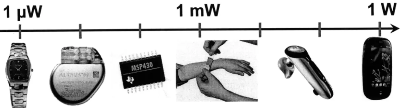
comparator reconfigurability. Redundancy factor refers to the number of comparators assigned to a given threshold. Additional comparators are placed at the edges of the input range to compensate for edge effects. INL values are not corrected for gain and offset errors. .... 38 2-4 Block diagram of the flash ADC. . ... . 39 2-5 Four possible circuit implementations for the sampling network. All
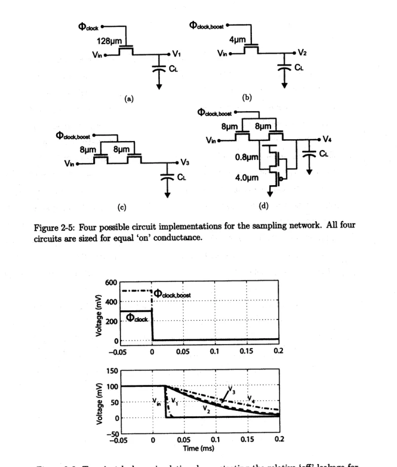
2-6 Transient leakage simulation demonstrating the relative 'off' leakage for the four sampling switch options presented in Figure 2-5. V1, 2,
V3, and V4 correspond to the nodes labeled in Figure 2-5. Simulation
results are for typical devices at 100'C. . ... 41 2-7 Circuit schematic for voltage boosting circuit. . ... 43 2-8 Comparator schematic. The comparator consists of many stacked
PMOS devices, each of which consists of a variable number of minimum-sized PMOS devices in parallel. ... .. ... . 44 2-9 Multiple NMOS transistors stacked. All nodes are initially precharged
to VDD. ... ... ... 46
2-10 Transient (a) ODE and (b) piecewise linear solution for V1, V2, ..., Vo0 for ten stacked NMOS transistors. . ... . 47 2-11 Block diagram of 127 by 9-bit memory with embedded counters used
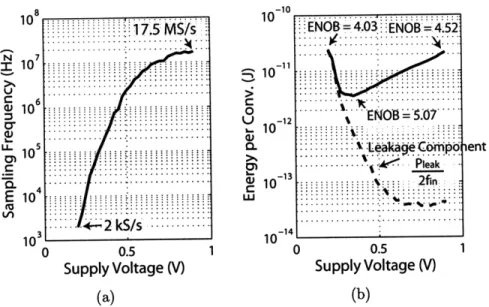
for calculating the estimated cumulative distribution function (CDF) of comparator thresholds. . ... ... 49 2-12 Die micrograph of the ADC in 0.18 pm CMOS. . ... 50 2-13 (a) Maximum sampling frequency and (b) energy per conversion versus
supply voltage, indicating presence of minimum energy per conversion at VDD = 0.4 V. ... ... ... 51 2-14 INL and DNL of ADC in single-ended 6-bit mode at VDD = 0.4 V. 51 2-15 FFT of ADC in (a) single-ended and (b) pseudo-differential 6-bit mode
at VDD = 0.4 V. ... ... 52
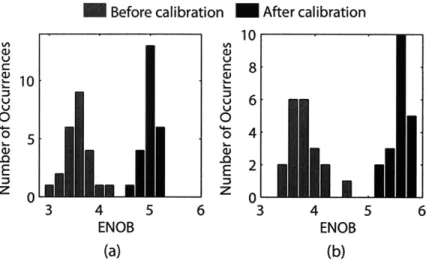
2-16 Statistical variation of ENOB in (a) single-ended and (b) pseudo-differential mode at VDD = 0.4 V before and after calibration. .... 53 3-1 Receiver energy/bit values vs. data rate for UWB and narrowband
receivers recently published at ISSCC [4]. Data for this plot are found in Table 5.4. ... ... 64 3-2 Three-channel frequency plan and narrowband interferers. . ... 64 3-3 Packet structure and receiver states for the wireless link. . ... . 65
3-4 Simplified block diagram of (a) receiver and (b) transmitter that form
the custom low-data-rate transceiver system. . ... 66
3-5 Transmitter expanded block diagram. . ... 67
3-6 Digitally controlled oscillator schematic. . ... 69
3-7 Die photo of fabricated transmitter. . ... 71
3-8 Measured transient waveform of a burst of five individually BPSK-modulated pulses ... ... ... .. 71
3-9 Overlaid power spectral densities of the three channels in the low-band of the 802.15.4a proposal. ... 72
4-1 Detailed block diagram of receiver SoC. . ... . 74
4-2 Block diagram of noncoherent UWB receiver presented in [4]... . 75
4-3 Circuit schematic of (a) resonant and (b) non-resonant amplifiers with equal power consumption. Simulation results comparing the gain of the amplifiers are presented in Figure 4-4. . ... 78
4-4 Gain of the resonant and non-resonant RF amplifiers presented in Fig-ure 4-3. ... ... 79
4-5 Four possible implementations of an RF gain stage with a resonant load. 80 4-6 Gain of an NMOS-based RF amplifier operating at 0.57 V (Fig. 4-5(a)), an NMOS-based cascode RF amplifier operating at 1 V (Fig. 4-5(b)), and an inverter-based, complementary RF amplifier operating at 1 V (Fig. 4-5(d)), with all amplifiers consuming equal power. . ... 82
4-7 Digitally tunable load capacitor of RF amplifier. All NMOS devices are minimum length and their width is shown. . ... 83
4-8 Schematic showing how differential signals can be leveraged to reduce transistor size. The two circuits shown have the same radio-frequency (RF) impedance, but by connecting a transistor between the positive and negative terminals, the overall transistor width is reduced by four times. ... ... . ... 83
4-10 Schematic of 6-stage RF amplifier, including the LNA. A variable num-ber of stages can be enabled depending on the gain required. ... 85 4-11 Schematic of differential, passive squarer. . ... . . 86 4-12 Output amplitude magnitude of differential squarer versus amplitude
of 4.5 GHz RF input. ... . . . ... 87 4-13 Transient simulation of RF front end at its maximum gain setting and
squarer in response to a pulsed LNA RF input. . ... 88 4-14 Baseband signal chain, consisting of a baseband amplifier, an ADC and
digital calibration logic ... ... 89 4-15 Examples of offset compensation approaches for the baseband
ampli-fier. (a) Discrete-time, analog offset compensation, (b) Continuous-time, analog offset compensation, and (c) Discrete-Continuous-time, digital offset
compensation ... ... .. ... 90
4-16 Circuit of current-mode DAC that is used to cancel baseband amplifier offsets ... ... .... .. ... ... 92 4-17 Table showing relationship between digital-to-analog converter (DAC)
code and current routing. Based on the DAC code, the DAC En-able/4:0] and Plus/Minus switches are opened or closed (Figure 4-16). In the table, shaded cells correspond to a switch being closed. .... 94 4-18 Two example circuits implementing a windowed integrator: (a) an op
amp based integrator, and (b) a transconductor based integrator. In both integrators, 01 controls a switch that resets the integrator output. 94 4-19 An example implementation of a time interleaved integrator and ADC.
Shown below the circuit diagram is a timing diagram. . ... 96 4-20 An example implementation of a cascaded integrator and ADC. Shown
below the circuit diagram is a timing diagram. . ... 97 4-21 Six stage cascaded integrator and ADC. . ... 98 4-22 Integrator and ADC clocking circuit that generates the level sensitive
4-23 Transient simulation of integrator and ADC for two integration pe-riods. The first integration period begins at 10 ns and the second
integration period begins at 42 ns ... 102
4-24 Pierce one-transistor crystal oscillator with amplitude control circuitry. 104 4-25 Pierce two-transistor, inverter-based, crystal oscillator. ... 104
4-26 Crystal oscillator output buffer, to amplify the oscillator output to full digital levels. ... 104
4-27 Delay-locked loop ... 105
4-28 RF output buffer to drive the amplified RF signal off-chip. ... 108
5-1 Die photograph of pulsed UWB receiver SoC. ... . 110
5-2 Bare die packaged in (a) a 40-pin QFN package and (b) a 64-pin QFN package. The 40-pin QFN package is 6mm x 6mm and the 64-pin QFN package is 9mm x 9mm. The two photos are equally scaled... 111
5-3 Block diagram of the three PCBs used for testing the receiver. ... 112
5-4 Opal Kelly XEM3001 FPGA module. (Actual size 3.5" by 2.0") .. . 113
5-5 Middle PCB of three PCB stack. (Actual size 4.5" by 2.4") ... 113
5-6 Top PCB (daughterboard) of three PCB stack. This specific daugh-terboard is designed for the 40-pin QFN package. (Actual size 1.8" by 1.3") ... ... 113
5-7 Test setup used to measure the BER of the receiver both with and without narrowband interferers. ... .. 115
5-8 BER of receiver (a) at its highest gain setting at the three center fre-quencies, and (b) at the different gain settings with f, = 4.0 GHz. .. 116
5-9 Sensitivity of the receiver versus core supply voltage at its highest gain setting (f, = 4.0 GHz) ... ... 117 5-10 Two comparison plots of receiver with previously published work: (a)
energy/bit versus data rate, and (b) normalized sensitivity versus en-ergy/bit. In both plots, a point is shown for the receiver at its highest
5-11 Top level block diagram of the UWB wireless image transmission sys-tem. (Courtesy Helen Liang) . ... .... 123 5-12 Measured sil of the receiver, comparing results from the 40-pin and
64-pin QFN packages and comparing a microstrip transmission line to a grounded coplanar waveguide transmission line. In all three configu-rations the receiver is tuned to a frequency of 3.5 GHz. ... . 124 5-13 Measured sil of the receiver with a center frequency of 3.5, 4.0 and
4.5 GHz packaged in a 40-pin QFN package with grounded coplanar waveguide transmission lines. . ... ... 125 5-14 Output spectrum of the RF front end when the low noise amplifier
(LNA) input is terminated to 50 Q. The spectrum analyzer RBW and VBW are set to 3 MHz, and the detector is set to average mode. . . . 126 5-15 Frequency dependent gain of the RF front end at its maximum gain
setting at the three channel frequencies ... 127 5-16 Output amplitude vs. input amplitude of the receiver RF front end at
its highest gain setting, with an input frequency of 4 GHz. From this plot, the PdB at the highest gain setting is measured to be -41 dBm. 128 5-17 Noise figure of the RF front end when operating in each of three channels. 129 5-18 Positive and negative output amplitudes of the squarer versus LNA
input power at its third of six RF gain settings (fc = 4.0 GHz). . .. 130 5-19 Measured differential output amplitude of the squarer versus LNA
in-put power for the six RF gain settings. . ... 131 5-20 Differential output amplitude of the squarer versus LNA input power
at its third of six RF gain settings, demonstrating a linear relationship between input power and output amplitude (f, = 4.0 GHz). ... 132 5-21 Differential output amplitude of the baseband amplifier versus LNA
input power for the six RF gain settings (fc = 4.0 GHz). . ... 133 5-22 (a) DNL and (b) INL of integrator and ADC. . ... 133 5-23 Linearity of ADC when provided a pulse input of varying duration. . 134
5-24 (a) DNL and (b) INL of DLL based on an LSB of i x 31.25 ns. The DNL and INL shown in (c) and (d) are based on an LSB of 2.04 ns. . 135 6-1 Lateral view of Manduca sexta moth attempting to feed from an
ar-tificial flower. (Photo courtesy of Armin Hinterwirth, University of W ashington) ... .... .. ... 141 6-2 Photograph of two, 4-electrode tungsten probes. . ... 141 6-3 Measured abdominal deflection of a moth in response to pulse stimuli of
varying voltage and frequency. In (a), the voltage of stimulation pulses is varied. T represents the pulse period, N represents the number of pulses and D represents the duty cycle. In (b), the frequency of stimulation pulses is varied, for a 0.5 s burst of 2.5 V, 1 ms pulses. .. 142 6-4 Transient measurement of current delivered through a tungsten
elec-trode when applying a 2.5 V pulse with pulse duration of 1 ms. . . 143 6-5 Photos showing abdominal deflection of a moth in response to pulse
stimulus. The abdomen is shown (a) before pulse stimulus and (b) dur-ing a pulse stimulus of 2.5 V, 100 Hz with duty cycle of 10%. The radial lines on the graph paper are spaced 20, indicating a total abdominal deflection of 10. ... ... ... . 144 6-6 Hybrid-insect flight control system. . ... 144 6-7 Block diagram of electronics mounted on a flexible PCB and attached
to a moth ... ... 146
6-8 Flexible PCB (a) top, (b) bottom, and (c) side. . ... 146 6-9 Photo of the UWB receiver SoC and a Texas Instruments
microcon-troller vertically stacked in a single package. The UWB receiver SoC is placed on top of the microcontroller. . ... 148 6-10 Block diagram of stimulation logic included in the UWB receiver SoC. 149 6-11 Photo of the moth with (a) dorsal PCB mounting and (b) ventral PCB
6-12 Photos of the surgical procedure to attach the hardware to the moth. In (a), the harness is attached to the moth and in (b), the tungsten probe is inserted through the cuticle into the connective tissue adjacent to the nerve connectives. . ... ... 151 6-13 Photograph of wind tunnel where moth flight tests were conducted. . 152 6-14 Time-lapse photos of a moth in a wind tunnel responding to pulse
stimulus. Pulse stimulus is generated by the receiver SoC after the receiver successfully decodes a transmitted packet. Photos of the moth are shown (a) prior to stimulation, (b) at the moment when stimulation begins, (c) when the moth's flight path begins to respond to the pulses, and (d) after having responded to the stimulation pulses. In response to the stimulation pulses, the moth's flight path turns to the left. . . 154 A-1 Propagation delay versus number of stacked NMOS devices for ODE
List of Tables
1.1 Example existing and emerging applications for energy constrained mo-bile devices ... .. . ... . 22 2.1 Summary of Results for ADC. . ... ... 50 3.1 FCC emissions limit for indoor and outdoor UWB communication... 58 5.1 List of pad connections on receiver SoC. . ... 110 5.2 Out-of-band interference robustness. . ... 118 5.3 Receiver power consumption breakdown. In idle mode, the crystal
oscillator is enabled. ... .. 118 5.4 Comparison of receiver with previously published work... 121 5.5 Crystal oscillator frequency for different chips, supply voltages and
oscillator topologies ... .. 135 5.6 Crystal oscillator phase noise at various offset frequencies for both
one-transistor and two-one-transistor Pierce oscillator topologies. ... . 135 6.1 Weight breakdown of components attached to the moth. . ... 148 6.2 Comparison between this work and previous published wireless
Chapter 1
Introduction
Mobile, battery powered devices have for decades fueled growth in the semiconductor industry. One of the defining moments in the semiconductor industry that kick-started this rapid growth was the invention of the integrated circuit by Jack Kilby in 1958 [5]. Whereas previous electronic circuits consisted of several discrete semi-conductor devices, integrated circuits allowed for multiple semisemi-conductor devices to be manufactured within a single piece of material, resulting a significant reduction in area and increased reliability. These benefits enabled many portable, battery pow-ered devices beginning with the handheld calculator, which was designed by Texas Instruments in the late 1960's and first sold by Canon in 1970 as the 'Pocketronic' [6]. A second key invention that has contributed to the growth of portable electronic devices was the invention of CMOS technology in 1963 [7], which allowed for a signifi-cant improvement in the energy efficiency of digital and analog circuits. Early CMOS powered mobile devices included low power wrist watches [8] and calculators [9]. Since then, CMOS processes have continued to improve and scale, following Moore's law, such that is now possible for a cellular phone to achieve comparable performance to a supercomputer of 30 years ago.
Wireless connectivity has been a key feature of portable devices, resulting in the exponential growth of cellular phones, now achieving annual sales of over one billion units. Laptop sales are now outnumbering desktop computer sales, and the emer-gence of the One Laptop per Child (OLPC) project and low cost 'sub-notebooks' will
1 mW
I I U
1-Figure 1-1: Spectrum of existing mobile devices micro-Watts to Watts.
that consume power ranging from
Table 1.1: Example existing and emerging applications for energy constrained mobile devices
Application Sensors Wireless Power Battery interfaces cons. lifetime
Wristwatch None None 1 pW Multiple years
[8]
Pacemaker Pacing leads Inductive link 10 AW 10 years [10]
Vital signs ECG, heart rate, 900 MHz ISM 1-8 mW 24 hours
monitor temperature (intensive care)
[11, 12]
Bluetooth Acoustic mic. Bluetooth 70 mW 6 hours
headset [13] (talk time)
Smart phone Acoustic mic., Bluetooth, 1 W 3-5 hours
[14] accelerometer, WiFi, GSM, (talk time)
camera HSDA, GPS
allow even greater penetration of portable, mobile devices. The majority of mobile devices consume power ranging from micro-Watts to tens of Watts, and a spectrum of applications are shown in Figure 1-1 and detailed in Table 1.1. In these applica-tions, energy is becoming more and more the limiting factor rather than performance.
This means that battery lifetime dictates performance specifications rather than per-formance dictating battery lifetime. This is particularly true for emerging systems such as implanted electronics. For example, roughly half the area of a pacemaker is occupied by a battery to ensure it can achieve 10 years of battery lifetime [10].
A conceptual diagram for a generic mobile device appears in Figure 1-2. The core components of the device include data conversion, signal processing, and
commu-1 pW
1W
Figure 1-2: Conceptual diagram of a generic mobile device.
nication subsystems, and these interface with the environment through sensors and actuators. Additionally, an energy subsystem is required to efficiently power the elec-tronics. This thesis focuses on the core mixed-signal components of a mobile device, namely the interface to the sensors, actuators and antenna via the analog-to-digital converter (ADC) and the wireless communication subsystem.
Four decades of Moore's law and semiconductor process scaling have made it pos-sible now to integrate billions of transistors on a single chip. With device geometries on the order of nanometers, device characteristics have changed so dramatically that many traditional circuits and architectures are no longer optimal and/or feasible. For example, reduced device breakdown voltages have forced circuits to operate at supply voltages near 1 V. As the number of dopant atoms per transistor decreases, random dopant fluctuations (RDFs) are becoming increasingly problematic, resulting in significant device variation. Subthreshold and gate leakage have increased relative to device's 'on' conductance such that leakage can no longer be ignored. These ex-amples are just a handful of the many challenges encountered with advanced CMOS processes, which have forced circuit designers to develop entirely new circuit topolo-gies and architectures.
An emerging trend in analog and mixed signal circuit design in nanometer-scale CMOS processes is the use of highly digital circuit topologies. There is no exact definition of what constitutes a highly digital circuit or architecture, but they can be broadly defined as consisting of significant digital logic, using simple 'digital'
struc-tures like comparators, switches, and capacitors, and using techniques like digital feedback. Such structures can be readily implemented in advanced CMOS processes whereas it is becoming increasing challenging to design 'analog' components such as op amps and employ techniques like analog feedback or analog offset storage.
This thesis is focused on developing highly digital, mixed signal circuits and ar-chitectures for energy-constrained mobile applications. As the spectrum of energy constrained devices is quite large, this thesis focuses specifically on the subset of de-vices that consume on average only a few milli-Watts or less, significantly less power than cellular phones. Typically, these low power devices require only a short-range (<100 m), low data rate (<100 kb/s) wireless radio and do not include power hungry components like an liquid crystal display (LCD).
To provide a broad perspective into highly digital circuits and architectures, this thesis is structured to progressively expand in scope, moving from a component level to a system-on-chip level and then finally to a full system demonstration. First, at the component level, a voltage scalable ADC is presented that operates from 0.2 V to 0.9 V and consists of almost entirely digital logic and comparators. Next, at the system-on-chip level, a wireless ultra-wideband (UWB) transceiver chipset designed in 90 nm CMOS is presented that achieves both high performance and low energy op-eration. The chipset includes an all-digital transmitter that employs an inverter-based power amplifier (PA) with capacitive combining to generate Federal Communications Commission (FCC) compliant, large output swing signals while consuming very little energy. Also included in the chipset is a fully integrated receiver system-on-chip (SoC) that leverages a simple, differential inverter-based RF front end combined with exten-sive digital calibration to realize robust operation in a miniature form factor system. Finally, the UWB transceiver chipset is demonstrated in a full system for insect flight control.
HP 10 10 10 3 Process Node (nm) (a) 0.4-HP 0 3 10 10 10 Process Node (nm) (b) ... . ... .. : 10 101 tP 10 2 3 10 102 103 Process Node (nm) (c)
Figure 1-3: Simulated effect of scaling on NMOS (a) Io/Ioff, (b) V/hVDD, and (c) g /g9d. For simulations, L = Lni, and W = 3Lmn. Device models include MOSIS provided models [1] and Predictive Technology Models (PTMs) [2, 3]. Both high performance (HP) and low power (LP) MOSFET data is shown.
1.1
Process Scaling: Benefits and Challenges
A key driving force behind the growth in mobile, battery powered devices has been
semiconductor process scaling. The world's first supercomputer, the Cray-1, which was released in 1978, had a 16-bit processor that operated at 80 MHz, used 8 MB of memory, weighed 5.5 tons and consumed about 115 kW of power [15]. Modern embedded processors, like the Marvell PXA320 XScale processor used in the LG-KC1 smartphone, realize superior performance than the Cray-1 while occupying board space equivalent to a credit card and require sub-1 W power consumption [16]. These dramatic reductions in energy and volume along with increased functionality have led to the emergence of highly complex mixed-signal SoCs.
A key challenge associated with semiconductor process scaling, however, is that
traditional circuit architectures are not compatible with nanometer-scale processes. Traditional architectures are either inefficient, negating many advantages of scaling, or cannot function properly. Circuit designers must overcome severe local and global process variation, increased gate and subthreshold leakage currents, reduced supply voltages, and reduced intrinsic gain of devices.
Figure 1-3 shows three separate plots of how transistor properties fundamentally change in advanced process nodes, each of which highlights a different challenge facing nanometer-scale CMOS circuit design. In Figure 1-3(a), lon/Ioff is shown to rapidly decrease in advanced CMOS processes, which can result in significant power consump-tion when circuits are disabled and also making it challenging to hold analog voltages on capacitors. In Figure 1-3(b), the ratio of device threshold voltage, Vth, to sup-ply voltage, VDD, increases with scaling, which effectively reduces voltage headroom and makes it difficult to stack multiple devices and employ techniques like cascod-ing. Voltage headroom is also reduced due to the fact that Vdsat does not scale with
VDD. In Figure 1-3(c), the gm/gds of CMOS devices is shown to decrease in advanced processes, making it difficult to obtain a large gain in single-stage amplifiers.
The data from Figure 1-3 is derived from Predictive Technology Models (PTMs) [2, 3] for 16 nm to 180 nm processes, and from MOSIS provided models for 0.25 pm, 0.35 pm, and 0.5 pm processes [1]. For the 16 nm to 45 nm processes, both high per-formance (HP) and low power (LP) device models are used. It is seen that a significant reduction in leakage can be achieved by using the low power devices, but Vth/VDD increases, reducing speed and decreasing voltage headroom. All simulations are with minimum length NMOS devices with a width three times the minimum length. In advanced processes, it is possible to increase gm/9ds by increasing the device length, but this results in the transistor area and gate capacitance to increase, removing some of the advantages of scaling. For leakage measurements in Figure 1-3(a), the NMOS devices are operated at the nominal supply voltage, which increases with older pro-cesses. The measurements in Figures 1-3(b) and 1-3(c) are based on diode-connected
NMOS devices each supplied 1 pA of current.
One additional problem associated with advanced CMOS processes that is not shown in Figure 1-3 is increased device variation, due to RDF and processing variation [17]. Both of these effects significantly change the resulting threshold voltage of devices and in a 65 nm process it has been shown that a ±4u variation from RDF alone can result in a change in drain-current by over three orders of magnitude [17]. Device variation most acutely affects digital circuits and memory, where devices are
typically minimum-sized to reduce area. In contrast, transistors in analog circuits are typically not minimum-sized because the devices consume minimal area relative to passive components such as capacitors and inductors, which are not subject to RDF. Moreover, analog transistors are often sized for biasing and noise constraints that result in relatively large devices.
1.2
Highly Digital Circuits
An emerging design approach that offers much promise to address many of the prob-lems associated with advanced semiconductor processes is the use of highly digital, variation-tolerant circuits and architectures. As described earlier in this chapter, highly digital circuits and architectures can be broadly defined as consisting of sig-nificant digital logic, using simple 'digital' structures like comparators, switches, and capacitors, and using techniques like digital feedback.
Highly digital circuits and architectures are the subject of this thesis with a focus on the design of highly digital ADCs and UWB wireless circuits for energy con-strained applications. The circuits and systems presented are designed to leverage the benefits of advanced nanometer-scale CMOS processes while overcoming the many challenges faced. The following sub-sections briefly introduce both ADCs and wireless transceivers, and provide some background into existing highly digital circuits and architectures.
1.2.1
Analog to Digital Converters
In systems that interface with the physical world, such as sensors or wireless radios, signals must be converted from the analog domain to the digital domain by an ADC so that they can be processed digitally and take advantage of the sophisticated ca-pabilities of a digital signal processor (DSP). Precisely how much processing is done before and after the ADC is a matter of system level optimization. ADC requirements depend on system characteristics, namely bandwidth and dynamic range, and system optimization must consider ADC power, which can be a significant portion of the total
power. As one might expect, the energy per conversion, which is an important metric for ADCs, increases as the dynamic range and sampling rate requirements increase. An empirical figure of merit (FoM) for ADCs normalizes their power consumption, P, to the input bandwidth, BW, and the dynamic range, expressed as 2ENOB (where
ENOB is the effective number of bits output) [18]:
FoM = (1.1)
2BW2ENOB
State-of-the-art converters today achieve an FoM as low as 4.4 fJ per conversion-step [19]; however, generally, dynamic ranges beyond those yielded by eight-bit con-verters have a steeper power increase due to device noise limitations in the ADC cir-cuits; the same is true when sampling-rates exceed tens of megahertz because devices must be biased further above their threshold voltage, VT, which results in degraded energy efficiency. In advanced CMOS technologies, the observed empirical trend has been that the FoM decreases by 1.8 times with each new process generation [20]. This trend in energy reduction offers significant incentive to develop highly digital ADC architectures customized for nanometer-scale CMOS processes. A few key emerging ADC trends are highlighted below.
Variation-tolerant ADCs. Mismatch and variation ultimately limit performance and yield of ADCs. There are several well known methods to reduce these effects, including increasing device sizes, common-centroid layout, auto-zeroing, cancelling offsets through feedback and redundancy. Of these, redundancy is a promising, emerg-ing technique that is well suited for highly scaled processes where more traditional methods are impractical and the selection of which devices to enable and disable can be implemented with simple digital switches and logic. Redundancy has been applied to SRAM sense-amplifiers to allow for reduced area and power compared to simply increasing the device size of a single sense-amplifier [21]. Redundancy offers much promise for highly-parallel systems, such as time-interleaved ADCs [22] or flash ADCs
[23].
design constraint and the supply voltage can be reduced to enable low energy opera-tion. Traditional analog circuit blocks cannot easily operate at low-voltages; however, a 0.5 V pipelined ADC has been demonstrated that uses operational transconduc-tance amplifiers (OTAs) biased in weak-inversion and does not require any voltage boosting [24]. A more prevalent way to realize low-voltage operation is through the use of highly digital ADC structures such as successive approximation register (SAR) ADCs. SAR is an excellent topology for micro-power low-voltage operation, as no lin-ear amplifiers are required for conversion. A 0.5 V SAR ADC has been demonstrated that achieves an FoM of 0.12 pJ per conversion step [25].
Comparator Based ADCs and Circuits. Comparator-based structures allow the implementation of switched-capacitor ADCs and analog circuits without the need for analog feedback - comparators replace the functionality of operational amplifiers by controlling energy transfer through comparator switching events rather than forcing a virtual ground through feedback. This approach offers potential for reduced power consumption and to address scaling issues in emerging technologies [20].
This thesis presents two ADCs that use these emerging trends to maximize energy-efficiency. A 6-bit flash ADC described in Chapter 2 leverages extensive comparator redundancy and reconfigurability to enable operation down to 0.2 V. A separate, 5-bit ADC described in Chapter 4, uses a multi-stage, dynamic integrator structure similar to an integrating ADC to generate the two bits of coarse quantization while a traditional flash ADC generates an additional three bits of fine quantization.
1.2.2
Wireless Transceivers
Wireless communication links found in energy constrained systems typically dominate the system's overall energy consumption. To reduce energy consumption, an emerging trend in radio design is to leverage highly digital architectures in advanced CMOS processes. There are several advantages associated with designing radios in advanced CMOS processes. One key advantage is that the radio can be integrated in a mixed-signal chip along with digital circuit blocks, thereby allowing for a highly compact implementation. A SoC radio, in which the RF, analog, and digital circuits are all
integrated on the same die offers the benefit of reduced parasitic capacitances between the many sub-blocks, thereby resulting in lower power consumption than a multi-chip solution. SoCs offer the additional opportunity for more flexible system-level optimization.
Much like low resolution ADCs, radios benefit from process scaling, particularly when the architecture is optimized for the process. Highly-digital radios offer sev-eral compelling advantages over traditional radio architectures in nanometer-scale processes. Nanometer-scale processes offer very low-impedance switches with low parasitic capacitance, thereby enabling highly reconfigurable and scalable radio ar-chitectures. Reconfigurability is becoming increasingly important as wireless devices are now being required to support multiple standards and frequency bands on a single-chip. This had led to a need for software-defined radios (SDRs), which can be reprogrammed when necessary to support a wide range of wireless standards [261. A separate benefit of process scaling is increasing device ft, which has resulted in untuned, non-resonant circuits becoming increasingly energy efficient such that they can be used in place of tuned, resonant circuits [271. These untuned circuits occupy significantly smaller area than tuned circuits.
UWB communication, technology that was first demonstrated by Marconi with spark gap transmitters, has recently gained traction in the research community in part due to its compatibility with advanced CMOS processes. UWB technology is a form of wireless communication in which signals occupy a wide bandwidth, greater than the lesser of 500 MHz or 20% of the center frequency of the signal, according to the FCC. There are several reasons why UWB communication is well suited to nanometer-scale CMOS and highly digital architectures. For high data rate UWB communication, operating at hundreds of Mb/s and above, only advanced CMOS processes are fast enough and sufficiently low power to decode and process the received bits. Addition-ally, due to the wide bandwidth of UWB signals, they can be efficiently amplified and processed with wide-bandwidth, low Q resonant or non-resonant circuits, which can be easily integrated on-chip with minimal area [28]. One specific method of UWB communication, termed impulse radio ultra-wideband (IR-UWB), is to encode data
in short pulses, on the order of nanoseconds. IR-UWB signaling is highly compati-ble with digital architectures, and very simple digital pulse transmitters consisting of only digital logic and delay elements have been successfully demonstrated [29].
1.3
Thesis Contributions
This thesis broadly examines the design of highly digital, mixed-signal circuits and architectures focusing on ADCs and UWB wireless transceivers. The scope of this thesis slowly expands, moving from a component level to a system-on-chip level and then finally to a full system demonstration. The main contributions of this thesis are in the following five areas.
1. Voltage/frequency scalable ADC - This thesis presents a voltage scalable flash ADC that can operate down to a supply voltage of 200 mV, which is the lowest reported operating voltage for a Nyquist rate ADC [30]. To achieve such low supply voltage operation requires a highly digital architecture that leverages redundancy to improve linearity and yield. Several circuit techniques are used to reduce the effects of leakage and the ADC implements common-mode feedback digitally.
2. Analysis of stacking in subthreshold regime - Due to comparator redundancy in the voltage scalable flash ADC, significant variation in the comparator's switch-ing thresholds can be tolerate. This allows for the use of a non-traditional com-parator, where the switching voltage is set through device stacking. This thesis presents an analysis of device stacking in the subthreshold regime, demonstrat-ing that stackdemonstrat-ing results in a quadratic change in effective device strength. 3. All-digital UWB transmitter - Two key problems inherent in many low power
UWB transmitters are that they either are not compliant with the FCC spectral mask without off-chip filters [29] or the output pulse amplitude is extremely low, fundamentally limiting range [31, 32]. A highly digital IR-UWB transmitter is
presented that employs capacitive combining to generate large pulse amplitudes that are FCC compliant while being energy efficient [33].
4. Highly integrated, noncoherent UWB receiver SoC - UWB receivers are tradi-tionally more complex than transmitters, and it is particularly challenging to achieve low energy, high performance operation in a highly integrated form fac-tor. This thesis presents the first fully integrated noncoherent UWB receiver with embedded synchronization logic [34, 35]. The receiver employs several highly digital amplifier and ADC structures, combined with extensive digital calibration to realize robust, low-energy operation in a 90 nm CMOS process. 5. System demonstration of UWB chipset for moth flight control - Insect flight
control is an emerging area of research where electronics and microelectrome-chanical systems (MEMS) are placed on and within insects to wirelessly control their flight. This thesis presents the first high performance radio that has been successfully demonstrated in wireless flight control of a moth. In this prelim-inary demonstration, the receiver SoC is implemented on a miniature, battery powered printed circuit board (PCB) weighing only 1 g and consuming only a few milli-Watts of average power.
1.4
Thesis Outline
The topic of this thesis is on the design of highly digital mixed-signal circuits and architectures. The thesis is structured to slowly expand in scope, moving from a component level to a system-on-chip level and then finally to a full system demon-stration. Chapter 2 focuses on a specific component, an ADC, describing a voltage and frequency scalable flash ADC. While this specific ADC is not used in the re-mainder of the thesis, the chapter highlights several highly digital design techniques,
some of which are used later. Next, the thesis moves to the SoC level, describing a UWB transceiver chipset. Chapter 3 introduces the low data rate UWB architecture and presents a highly digital transmitter. The receiver SoC circuits and measurement
results are presented in Chapters 4 and 5, respectively. Finally, the thesis presents a system demonstration of the UWB transceiver chipset in Chapter 6, in an insect flight control system. Conclusions and a discussion of future work are presented in Chapter 7.
Chapter 2
Highly Digital, Voltage Scalable
ADC
Microsensor wireless networks and implanted biomedical devices have emerged as exciting new application domains. These applications are highly energy constrained and require flexible, integrated, energy-efficient ADC modules that can ideally operate at the same supply voltage as digital circuits. In many applications, the performance requirements are quite modest (-100 kS/s). In systems with extensive digital signal processing, an additional demand faced by these ADCs is that they be compatible with advanced digital CMOS processes. As CMOS processes advance, digital switching energy reduces and scaling allows for increasingly complex algorithms with minimal energy overhead but key challenges such as increased leakage and device variation emerge.
In recent years, highly digital ADC architectures like SAR and EA modulators have gained popularity due to their compatibility with advanced CMOS processes. In [36], a frequency-to-digital EA modulator is presented that uses only inverters and digital logic gates, operating at a supply voltage of 0.2 V. In many of these ADCs, the overall digital (CV2) power consumption is greater than analog power consumption,
allowing for significant digital energy savings through voltage scaling. Voltage scal-ing can also be applied to analog circuits to reduce power consumption, particularly in low-resolution ADCs where thermal noise is not a limiting constraint; however,
Voltage
\
Digital
Digital
In
Logic
Out
Enable Inverters
Figure 2-1: Conceptual block-diagram of an inverter-based ADC.
care must be taken to minimize the impact of power supply noise. Moreover, when operating analog circuits at low supply voltages, device leakage and variation, al-ready serious concerns in advanced CMOS processes, become increasingly severe and traditional circuits and architectures are often impractical. To overcome these chal-lenges, highly digital architectures must be employed and combined with techniques like redundancy and reconfigurability.
Inspired by the aforementioned scaling trends, much research has focused on re-alizing highly digital ADCs with the ultimate goal of a synthesizable ADC. Imagine, for instance, a highly digital flash ADC consisting solely of a sea of many redundant and reconfigurable inverter-based comparators combined with digital backend logic for calibration, as shown in Figure 2-1. Due to the redundancy, there are a very large number of comparators, and during normal operation only a small subset of the comparators are enabled. This extreme redundancy allows for the tolerance of large comparator voltage offsets. In a flash ADC reconfigurability can be combined with redundancy to allow any comparator to be assigned to any ADC threshold. If, after calibration, only a subset of inverters are enabled such that their switching thresholds are linearly spaced, an energy efficient, highly digital ADC can be realized.
This chapter presents a highly-digital, voltage scalable flash ADC implemented in a 0.18 pm CMOS process, inspired by the vision of an inverter-based ADC [30]. Section 2.1 describes the ADC architecture highlighting how redundancy and recon-figurability is used to improve linearity and how extensive processing is moved to the digital domain. Section 2.2 presents the key ADC circuit blocks, including the
front-end sampling switch and the clocked comparator array. Transistor sizing and stacking are used to vary comparator switching thresholds, and a mathematical analysis of the relationship between transistor stacking and comparator switching thresholds in the subthreshold regime is presented. Finally, measurement results are presented in Sec-tion 2.3.
2.1
ADC Architecture
2.1.1
Background and Theory
To achieve energy efficiency, the ADC presented in this chapter is designed to operate at low voltages, where the energy per conversion is minimized. This operating voltage is akin to the minimum energy point for digital circuits [37] and is based on the assumption that the ADC sample rate scales with varying supply voltages. For ADCs, the energy per conversion is minimized when the sum of leakage energy and active energy is minimized, which for the ADC presented in this chapter occurs at supply voltages near MOSFET threshold voltages. Low voltage operation allows for improved energy efficiency but limits the maximum operating frequency. If higher operating frequencies and input bandwidths are required, interleaving and parallelism can be used to recover performance [22]. Low voltage operation also causes many analog design challenges that must be addressed. Two key architectural challenges are that increased variation in the subthreshold regime causes significant comparators offsets, and that traditional differential architectures are impractical.
A key block in flash ADCs is the comparator network, including the peripheral circuitry that ensures each comparator has an appropriate switching threshold. In traditional flash ADCs, where there is a 1:1 correspondence between comparator and output code, the combined comparator and reference voltage offset must be significantly less than 1 least significant bit (LSB) to ensure a reasonable linearity. For example, assuming a Gaussian distribution, a 6-bit ADC requires an offset, aoffset to be smaller than 0.2 LSB to achieve a 99% yield of INL < 1 LSB [38]. Maintaining
Code
Code
6 --- a- b--6b --c-- 6 0 5 --- 5a---Sb --- 5c-- -0 5 5a '----o ) 4 --- 4a---4b ---4c-- o 4 --- -- - --- i--- -1 ---3a---t-3b--- -- 1 ---1c (a) (b)Figure 2-2: (a) Nominal threshold voltage of comparators for a 6-level, flash ADC with three redundant comparators at each threshold voltage. (b) Example of the ADC with threshold variation. The comparators that are selected after calibration are highlighted.
low offsets requires large transistors, resulting in significant parasitic capacitance and area. Alternatively, offsets can be cancelled through analog and mixed-signal techniques such as a feedback DAC [39, 40] or correlated double sampling (CDS) [41]. In [40], large offsets in a flash ADC preamplifier are cancelled by embedding a 5-bit DAC within each preamplifier.
As it is difficult to realize analog offset compensation at low supply voltages, the ADC architecture leverages digital calibration combined with redundancy [23]. Many redundant digital regenerative comparators with large input-referred offset variation are used in place of a small number of precise comparators and reference voltages. Any comparator can be assigned to any specific threshold, and there are many more comparators available than thresholds required. By increasing the number of redun-dant comparators, the ADC can achieve the required yield even in the presence of very large variation in each comparator's threshold, with a standard deviation, a,
much larger than one LSB.
Figure 2-2 graphically demonstrates how redundancy and reconfigurability are used by the flash ADC. In the figure, the comparator threshold voltages of a 6-level flash ADC are shown where three comparators are inserted for each threshold voltage. Figure 2-2(a) shows the comparator thresholds when there is no comparator threshold variation. In this situation, the redundancy and reconfigurability is not needed.
Fig-ure 2-2(b) shows the comparator thresholds in the presence of comparator threshold variation. The comparators that are selected after calibration are highlighted. In the example, comparator 2b has a significant voltage offset, but is selected to represent the fourth switching threshold. There is no comparator that perfectly aligns with the fifth switching threshold, so the closest comparator, 5c, is selected.
The concept of comparator redundancy and reconfigurability can be analyzed numerically to gain a quantitative understanding of the relationship between redun-dancy and yield. Whereas when a < 1 LSB, the probability distribution of indi-vidual comparator thresholds are narrow around their respective mean thresholds; when a > 1 LSB, the probability distribution of individual comparator thresholds significantly overlaps those of comparators with nearby thresholds. In this scenario (a > 1 LSB), the number of comparators within a given voltage range is proportional to the size of the voltage range, ignoring edge effects at the boundaries of the input range. Thus, the thresholds are Poisson distributed. If we assume N comparator thresholds over an input range of Vdr, and a redundancy factor of R, the probability that there are no thresholds within a voltage range of x can be calculated to be:
xNR
Probability = e Vdr (2.1)
From this equation, we can calculate the expected probability that INL < 1 LSB, assuming no correction for gain and offset errors. Here, INL is defined as the maximum difference between the ideal and actual code transition levels after correcting for gain and offset [42]. When INL < 1 LSB, there cannot be a gap of
+1
LSB around each of the N ideal switching thresholds (or code transition levels) with no comparator thresholds, and thus x = 2vr. Thus, the following approximation for INL is derived:Probability (INL > 1 LSB) e Ne-2
R (2.2)
This approximation is only valid when e-2
R < 1. The approximation is presented
in Figure 2-3 along with Monte Carlo results showing how redundancy and reconfig-urability can be combined to achieve a required linearity and yield in the presence of
* No reconfig, o=2
* Reconfig up to 1 LSB, 0=3
V Full reconfig, c=3
- Approximation for full reconfig.
-2
10
...
-4z10
V
0 -611106
0-0
5
10
15
Redundancy Factor, R
Figure 2-3: Yield of ADC versus redundancy factor for ADCs with varying levels of comparator reconfigurability. Redundancy factor refers to the number of comparators assigned to a given threshold. Additional comparators are placed at the edges of the input range to compensate for edge effects. INL values are not corrected for gain and offset errors.
large comparator threshold variation (a >1 LSB). In the Monte Carlo simulations, no offset error and no gain error are tolerated. The ADC yield can significantly improve if offset and gain errors are tolerated. As edge effects reduce yield, addi-tional comparators are inserted with switching thresholds at the edges of the input range. Compared to increasing device sizes, redundancy and reconfigurability have been shown to offer an improved trade-off between power/area and linearity [231.
2.1.2
Overview
Figure 2-4 shows a block diagram of the ADC. The ADC can be configured in either a single-ended or pseudo-differential configuration. It consists of a sampling network, two arrays of 127 dynamic digital clocked comparators and a digital backend. Instead of a traditional reference ladder that draws static current, the ADC uses dynamic comparators with static voltage offsets to generate comparator thresholds. The digital dynamic comparators are based on a sense-amplifier flip-flop and are described in detail in Section 2.2. The digital backend consists of two 127-bit Wallace
Clocked Wallace
Comparators Adder
o 127
"0 . 12712 127x9b memory
Vin,.-,
'@ Calibration logic126
Low-Leakage Enable[126:0]
Sampling Switch , 1 Digital
C M Rej. - Out
IIR Filter
Vin-o
o.7127x9b memory126 Vn 7 Calibration logic
T
Enable[126:0] 127Figure 2-4: Block diagram of the flash ADC.
tree adders, two on-chip 127 x 9b memories with calibration logic, and an infinite-impulse response (IIR) common-mode rejection filter. The Wallace tree adders sum the individual thermometer encoded comparator outputs and generate binary values. The ADC is designed for a maximum of 6-bits of resolution, so in nominal mode no more than 63 comparators are enabled, and 64 comparators are disabled. For this implementation, a redundancy factor of 2 was used to reduce area overhead at the cost of degraded linearity when compared to an ADC with higher redundancy factor. Before nominal operation can commence, the ADC must be calibrated by applying an input with known distribution such as a triangle wave. In single-ended mode, calibration can be applied in a ping-pong process, whereas in pseudo-differential mode calibration must be foreground. While calibrating, the Wallace tree adder is bypassed and each comparator is assigned to a specific 9-bit accumulator. An estimate of the CDF of the input is generated in on-chip memory, and the comparator thresholds are back-calculated from this data off-chip. Based on these thresholds, an off-chip algorithm determines which comparators to enable. Once the appropriate subset of comparators are enabled, the ADC can operate in nominal mode with the output code taken at the output of the Wallace tree adders.