HAL Id: tel-01931464
https://tel.archives-ouvertes.fr/tel-01931464
Submitted on 22 Nov 2018HAL is a multi-disciplinary open access archive for the deposit and dissemination of sci-entific research documents, whether they are pub-lished or not. The documents may come from teaching and research institutions in France or abroad, or from public or private research centers.
L’archive ouverte pluridisciplinaire HAL, est destinée au dépôt et à la diffusion de documents scientifiques de niveau recherche, publiés ou non, émanant des établissements d’enseignement et de recherche français ou étrangers, des laboratoires publics ou privés.
Probing chalcogenide films by advanced X-ray metrology
for the semiconductor industry
Walter Batista Pessoa
To cite this version:
Walter Batista Pessoa. Probing chalcogenide films by advanced X-ray metrology for the semiconduc-tor industry. Micro and nanotechnologies/Microelectronics. Université Paris-Saclay, 2018. English. �NNT : 2018SACLS330�. �tel-01931464�
Acknowledgements 0
Probing chalcogenide films by
advanced X-ray metrology for the
semiconductor industry
Thèse de doctorat de l'Université Paris-Saclaypréparée à l’Université Paris-Sud
École doctorale n°576 : Particules hadrons énergie et noyau : instrumentation, image, cosmos et simulation (PHENIICS) Spécialité de doctorat : Physique des accélérateurs
Thèse présentée et soutenue à Grenoble, le 27 Septembre 2018, par
Walter Batista Pessoa
Composition du Jury : Anne Lafosse
Professeure, Institut des Sciences Moléculaires d'Orsay (ISMO)
Université Paris Sud Présidente
Philippe Jonnard
Directeur de recherche CNRS,
Laboratoire de Chimie Physique Matière et Rayonnement (LCPMR)
Sorbonne Université Rapporteur
Eugénie Martinez
Ingénieur-chercheur, Département Technologie Silicium (DTSi)
CEA-Laboratoire d’Electronique et de Technologie de l’Information (LETI) Rapporteuse Franck Delmotte
Maître des conférences, Laboratoire Charles Fabry (LCF)
Institut d'Optique - Université Paris Sud Examinateur
Paul Ryan
Director of Product Management
Bruker Semiconductor Division, UK Examinateur
Marie-Christine Lépy
Directrice de recherche CEA, Laboratoire National Henri Becquerel (LNHB)
CEA-Laboratoire d’Intégration de Systèmes et des Technologies (LIST) Directrice de thèse Emmanuel Nolot
Ingénieur-Chercheur, Département Technologie Silicium (DTSi)
CEA-Laboratoire d’Electronique et de Technologie de l’Information (LETI) Co-Encadrant de thèse Anne Roule
Ingénieure-Chercheur, Département Technologie Silicium (DTSi)
CEA-Laboratoire d’Electronique et de Technologie de l’Information (LETI) Co-Encadrante de thèse
NNT : 20 18 S A C LS 33 0
Acknowledgements 1
“Science is the search for truth, it is not a game
in which one tries to beat his opponent,
to do harm to others.”
Linus Pauling
Acknowledgements 2
Acknowledgements
First of all, I would like to express my gratitude to CEA-LETI and the Silicon Technology Division for giving me this opportunity to work in a unique cutting-edge facility forged by team-work spirit, multiculturalism and technology pioneering known worldwide.
I would like to express my deepest appreciation to my supervisors Emmanuel Nolot, Anne Roule and to my PhD directress Marie-Christine Lépy for the patience, kindness, expertise transfer and rigorousness to put me back on track the moments my research was going off the topic. This thesis would not be possible without you three, and each one of you had special role during this three years, you all known. I am deeply grateful to have you three as supervisors not only on the professional side but also on personal one, for all the laughs, good moments in the laboratories as well as in conferences, and I will always be in debt with you by assisting me in the hardest moments during my thesis.
I also would like to express my gratitude to Eugénie Martinez and Philippe Jonnard by accepting to be rapporteurs as well as devoting your attention to evaluate this work. I also would like to thank Anne Lafosse, Franck Delmotte and Paul Ryan by agreeing to be part of the jury and dedicating your time to exam my work.
I would like to offer my special thanks to Laurent Vandroux and Cécile Moulin by the kindness and warmly hosting me in the Deposition service (SDEP) of the Silicon Technology Division. I am also grateful for aiding me in my hardest moments in the thesis. In addition, this thesis would not be possible without the SDEP team in particular Chiara Sabbione, Mathieu Bernard and Walid Darwich for the film deposition, as well as, Agathe André, Sylvie Favier for the X-ray metrology help, and Pierre Noé, Rémy Gassilloud and François Martin for the chalcogenides expertise.
This thesis would be far from completed without the expertise and participation of the nano-characterization platform (PFNC) of LETI, Laboratoire des technologies de la Microélectronique (LTM), Laboratoire National Henri Becquere (LNHB), as well as the synchrotrons SOLEIL (Saclay, France), ELETTRA (Trieste, Italy). In particular, I would like to thank Patrice Gergaud, Francois Pierre, Jean-Paul Barnes from the PFNC, Bernard Pelissier and Sebastien Labau from the LTM, Yves Ménesguen, Jonathan Riffaud and Anastasiia Novikova from the LNHB, Paulo Da Silva and Pascal Mercere from Metrology beamline of SOLEIL synchrotron, Diane Eichert and Fabio Brigidi from the Fluorescence beamline of the ELETTRA synchrotron.
My sincere gratitude goes to Yan Mazel and Simona Torrengo who are not only great friends and sympathetic officemates but also actively contributed to complement my experiments. Also thank you Yan for teaching me creo, a dance from my own country that I never heard about it. And also thank you Simona for joining me in the synchrotron adventures in Saclay, the snow storm during the February campaign is unforgettable. Although the harsh during these campaigns, I will miss all laughs, nightshifts and Courtepaille moments.
I would like also to thank my former officemates Bérenger Caby, Hélène Rotella and Gaël Picot, not only for the kindness and sympathetic moments during my first year but also for the important GIXRF/XRR development the years before I arrive in LETI. I also would like to thank in special
Acknowledgements 3
Bérenger for being very kind friend and giving me moral support when things were becoming harsh. I want also to thank the déjeuner team Jérôme Richy, Vincent Huynh, Lauraz sauze, Myriam Le Guen and Victor Yon for being part of my PhD life, for all the laughs and coffees in the most important moment of the day. I also would like thank the Pierre Noe team Philippe Kowalczyk, Jean-Baptiste Dory and Rebecca Chahine for the friendship and also being part of my PhD life, in particular Philippe whom I could actively work together the first year. I also would like to thank all my SDEP friends and my PFNC friends for all the coffees and croissants every day. Finally, I would like to thank my family and my parents for the unconditional love and the support during these three years of doctoral work.
Summary 4
Summary
Acknowledgements ... 2 Summary ... 4 List of figures ... 11 List of tables ... 18 Acronym list ... 19 Introduction ... 221. Chapter I: Chalcogenide materials ... 24
1.1. Chalcogens Atomic Electronic configuration ... 25
1.2. 3D chalcogenide materials: ... 27
1.3. 2D chalcogenide materials ... 34
1.4. Scaling properties of chalcogenide materials ... 38
1.5. Synthesis of chalcogenide films ... 41
1.6. Motivations of this work ... 45
1.7. References ... 46
2. Chapter II: Probing chalcogenide materials... 49
2.1. Introduction ... 49
2.2. X-Ray and matter interactions ... 50
2.3. XRF quantitative analysis ... 55
2.4. Grazing Incident X-ray Fluorescence (GIXRF) ... 60
2.5. Photoelectron emission ... 69
2.6. Sources and instrumentation ... 86
2.7. X-Ray instruments employed in this work ... 97
2.8. Conclusions ... 101
2.9. References ... 102
3. Chapter III: Surface and interfaces protocols ... 104
3.1. Introduction ... 104
3.2. Probing Surface effects on Ge-Sb-Te films ... 105
3.3. Evaluation of capping efficiency as barrier layers ... 118
3.4. Conclusions ... 125
3.5. References ... 126
4. Chapter IV: Chemical quantification protocols ... 127
4.1. Introduction ... 127
4.2. Chemical quantification of Ge-Sb-Te film ... 128
4.3. Chemical quantification of N-doped Ge-Sb-Te films ... 144
4.4. Probing WSx films (2D Transitional Dichalcogenides) ... 151
4.5. References ... 165
5. Chapter V: Elementary depth profile protocols ... 167
5.1. Introduction ... 167
5.2. Probing TiTe films by GIXRF/XRR combined analysis... 168
Summary 5
5.4. Probing Te-based films by angle-resolved XPS ... 189
5.5. Conclusions ... 196
5.6. References ... 197
Conclusions ... 199
6. Annex A: Ion Beam analysis (IBA) ... 200
7. Annex B: Mass spectrometry techniques ... 204
8. List of publications ... 206
9. Résumé étendu en français ... 208
Abstract ... 213
List of figures
Figure 1.1. Tetrahedrally bonded semiconductors (left) and LP semiconductors (right). ... 25 Figure 1.2. St-John-Bloch plot demonstrating the ionicity (r’σ) and covalency (rπ-1) of IV-VI
compounds and group V elements [10]. ... 26 Figure 1.3. Ternary phase diagram for different phase-change alloys, and an inset highlighting the main years of PCM development [16] ... 27 Figure 1.4. Resistivity (a) and reflectivity (b) measured as function of increasing temperature for GeTe and Ge2Sb2Te5 films, amorphous phase correspond to high electrical resistivity and low optical
reflectivity, while crystalline phase is the contrary [16]. ... 28 Figure 1.5. Mapping phase-change materials according to their ionicity bonds (x axis) and tendency towards s-p hybridization (y aixs). We can clearly see very distinct bands of oxides, sulfides,
selenides, and telluride indicated as red, orange, yellow and green, respectively [21]. ... 28 Figure 1.6. (a) Transmission Electron Microscopy (TEM) Cross-sections of Ge-Sb-Te PCM-cell in a SET state (crystalline), while in (b) it is in RESET state (active zone in amorphous state). (c)
Schematically illustrates the process to SET and RESET the PCM-cell [15]. ... 29 Figure 1.7. Resistance-Current relation of a (GeTe)4(Sb2Te3)2 iPCM (red curve) and GeSbTe cells
(black curve). The upper plot corresponds to the first cycle of electrical switching, while the lower plot 106 cycles [23]. ... 30
Figure 1.8. Nano-scale Einstein image written by an ionic memory [29]. ... 31 Figure 1.9. Scheme highlighting the mechanisms procedure to SET (A-D) and RESET (E) in CBRAM cell [30]. ... 31 Figure 1.10. Use of photosensitive As2S3 chalcogenide film to tune the resonant frequency of a
photonic crystal cavity. (a) An image of the photonic crystal cavity and its optical response. (b) Schematic of the method used to tune cavity. (c) Cavity response as a function of illumination time for a 60 nm As2S3. (d) Tuning curves for two different thickness of the As2S3 film [39]. ... 33
Figure 1.11. (a) Typical stack configuration of thin-film solar cell. (b) Differences in the lattice constant and bandgap energy of absorbers (blue circles), buffers (black squares) and TCOs (red
triangles) [43]. ... 34 Figure 1.12. Atomic structure of single layers of transition metal dichalcogenides (TMDCs) in their trigonal prismatic (2H), distorted octahedral (1T) and dimerized (1Tʹ) phases. Lattice vectors and the stacking of atomic planes are indicated [44]. ... 35 Figure 1.13. Impact of the thickness reduction on the 2H MoS2 calculated bandgap [48]. ... 35
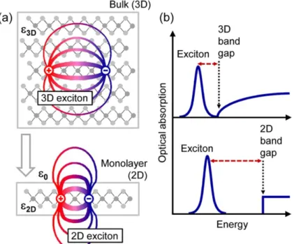
Figure 1.14. Circularly polarized EL spectra for two opposite current directions schematically indicated in the top illustration. Bottom illustration represent the contribution to EL from two valleys [48]. ... 36 Figure 1.15. (a) Real-Space representation of electrons and holes bound into excitons for the three-dimensional bulk and a quasi-two-three-dimensional monolayer. (b) Impact of the three-dimensionality on the electronic and excitonic properties, schematically represented by optical absorption [50]. ... 37 Figure 1.16. Local gate control of the MoS2 monolayer transistor. (a) Ids-Vtg curves recoded for a bias
voltage ranging from 10 to 500 mV. Inset Three-dimensional schematic view of one of the transistors. ... 37 Figure 1.17. (a) Crystallization temperatures Tx as a function of compositions in the Ge-Sb-Te ternary
phase diagram. (b) Resistivity as a function of temperature for Ge2Sb2Te5 and Ge modification of
Ge2SbTe2 films during a heating ramp to 400°C at 5°C/min and subsequent cooling back to
temperature [52]. ... 38 Figure 1.18. Evaluation of the crystallization temperature and activation energy for crystallization for N-doped GeTe thin films [56]. ... 39
List of figures 12
Figure 1.19. Phase-diagram of Cu intercalated TiSe2, of which transition among metal, charge density
wave (CDW) and superconductivity (SC) is presented [59]. ... 40
Figure 1.20. Evolution of crystallization temperature as a function of film thickness for various phase-change materials [61]. ... 41
Figure 1.21. (a) Variation of the band gaps as a function of the number layers (n). (b) Position of the band edge with respect to the vacuum level [62]. ... 42
Figure 1.22. Simulation effects of the increasing levels of resputtering highlight the formation of voids [63]. ... 42
Figure 1.23. Precursor and transport reaction [65]. ... 43
Figure 1.24. Procedure of MOCVD deposition. ... 44
Figure 1.25. Schematic illustration of an ALD cycle of HfO2 process where precursors, HCl4 and H2O are alternately pulsed and separated by inert gas purging. ... 45
Figure 2.1. The electromagnetic spectrum range, X-ray wavelength ranges from 12 to 0.012 nm between Ultraviolet and Gamma rays. ... 50
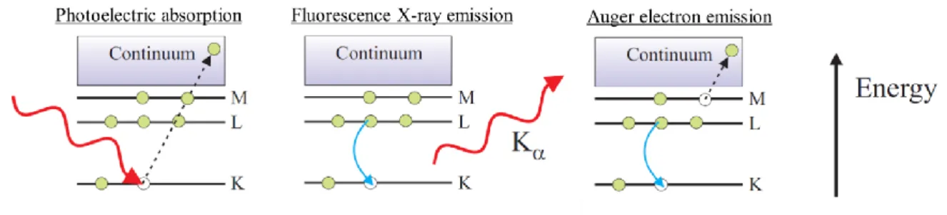
Figure 2.2. The photo-electric effect, and consecutive X-ray fluorescence, or Auger emission. ... 50
Figure 2.3. Energy levels of different subshells of an atom along with their quantum numbers and occupancy of electrons. ... 51
Figure 2.4. Energy levels of main X-ray fluorescence line series. ... 52
Figure 2.5. Elastic scattering. ... 53
Figure 2.6. Inelastic scattering ... 53
Figure 2.7. Absorption edges of tellurium [2]. ... 54
Figure 2.8. Fluorescence yields for K and L shells for 5 ≤ Z ≤ 110 [3]. ... 55
Figure 2.9. Empirical method and FP method sensitive curves. ... 56
Figure 2.10. X-Ray interacting with flat homogenous material. ... 56
Figure 2.11. Matrix effects, secondary and tertiary fluorescence process... 58
Figure 2.12. Cascade effects process triggering indirect excitation [7]. ... 58
Figure 2.13. Sensitive curve calculated from FP method from RIGAKU XRF software. ... 59
Figure 2.14. Characteristics form of the angular dependence of the fluorescence of thin layer and bulk substrate [8]. ... 60
Figure 2.15. Scheme of reflection and refraction for stratified homogenous media. ... 61
Figure 2.16. (a) Reflectivity and normalized (solid lines) penetration depth (dashed lines), (b) phase (solid lines) and normalized E-field intensity (dashed lines) [10]. ... 62
Figure 2.17(a) Normalized-height dependence of the normalized E-field intensity for different normalized incident q. (b) The normalized-angle dependence of the normalized E-field intensity for two different heights above the mirror surface [10]. ... 63
Figure 2.18. Reflection and refraction of the plane-waves at two successive boundaries in a multilayer. The boundaries are parallel and separate layers j-1, j and j+1 with indices of refraction nj-1>nj+1>nj 64 Figure 2.19. (a) 3-D schematic of the geometrical parameters in GIXRF experiments. (b) Reciprocal of G(θ) calculated for different widths Ld, with Ls 30 mm and b0 15 mm. (c) Influence of G(θ) in a Ti-Kα XRf intensity for a Si/Ti/Ni/Ti/Si(Sub) multilayer sample. ... 67
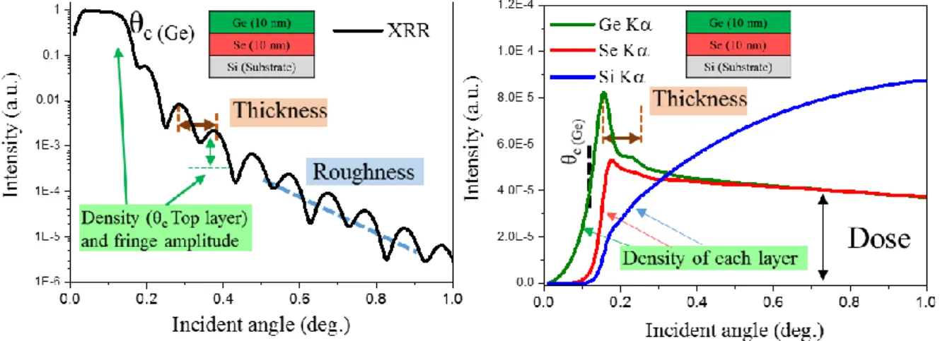
Figure 2.20. Probing wafers by XRR-GIXRF combined analysis, example of a multilayer Ge/Se/Si(Sub) stack. ... 68
Figure 2.21 Flowchart of typical GIXRF and XRR data simultaneously processed [18]. ... 69 Figure 2.22. Schematic process of photoelectron emission, the electron excited by the incident X-ray
List of figures 13
beam has to overcome the worth function ϕA to be measurable. ... 69
Figure 2.23. Survey spectra of tellurium oxide film. ... 70
Figure 2.24. Sb 3d core-level range, XPS high resolution spectra core level. Composition deduced from deconvolution based on spin-orbit split and intensity ratio. ... 71
Figure 2.25. Schematic mechanism of Auger electron emission. ... 72
Figure 2.26. Ni 2p3/2 –Ni LMM Wagner plot for Ni metal, Ni alloys, NiO, Ni(O/H)2 and NiOOH [24]. ... 72
Figure 2.27. (a) Insulators and conductors bands of materials, (b) Typical Valence spectra [25]. ... 73
Figure 2.28. Shake-up structure in Cu 2p of copper (II) oxide. ... 74
Figure 2.29. Plasmon loss structure in spectrum of aluminum metal [26]. ... 74
Figure 2.30. Influence of chemical shift on binding energy, elements with higher electronegativity induces compound to shift towards higher binding energies [27]. ... 75
Figure 2.31. Ge2p3/2 data processing is highly impacted by G/L deconvolution, for proper process a G/L mix has to be considered. ... 76
Figure 2.32. The complex Se3dspectra from a BiS2 film can be processed by spectra deconvolution [27]. ... 77
Figure 2.33. Comparison between linear and Shirley background. Shirley background properly modeled spectra range, while linear have some misleading range [27]. ... 78
Figure 2.34. Scofield values of cross-section σ for Al-Kα source. The values are referenced to C1s as 1.0 [31]. ... 80
Figure 2.35. The left trajectory is pure inelastic scattering, towards grazing angles elastic scattering increases the electron trajectory [26]. ... 81
Figure 2.36. Compilation of experimental attenuation lengths for inorganic compounds [34]. ... 82
Figure 2.37. (a) Sample depth as function of electron take-off electron θ, the width of the shaded areas represent the proportion of the detected electrons emitted as function of depth; (b) overlayer (A)/substrate(B) and intensity (I) versus θ. ... 83
Figure 2.38. Conventional ARXPS (right) requires tiltong the sample, while parallel ARXPS (left) perform analysis with sample stationary [37]. ... 84
Figure 2.39. ARXPS data processing by Max-entropy method reveals very consistent elementary depth profile with Sb/Te proportion close to theory (~2/3). ... 85
Figure 2.40. The average and peak brightness of photon beams at LCLS, ESRF, FEL, and some others advanced synchrotron sources [39]. ... 86
Figure 2.41. X-ray generation from a target. ... 87
Figure 2.42. Main types of X-ray laboratory sources as well as their respective brightness as a relation between power and apparent source. ... 88
Figure 2.43. Schematic synchrotron source (left), storage ring and magnets (right) for electron conditioning. ... 89
Figure 2.44. Monochromatization process by double monochroamtor (rigth) and focussing mirror (left). ... 89
Figure 2.45 . Schematic principle of EDXRF, spectra resolution (>150 eV). ... 90
Figure 2.46. Schematic principle of a WDXRF, spectra resolution (5 eV). ... 90
Figure 2.47. Schematic diagram of a SDD detector with n-channel Junction gate field-electric transistor (JFET), the transistor gate is connected to the anode ring by a metal strip [42]. ... 92
Figure 2.48. Detector efficiency of Silicon Drift Detector and High Purity Germanium detector, ... 94
List of figures 14
Figure 2.50. Structure of gas-flow proportional counter. ... 95
Figure 2.51. Schematic working principle of a XPS tool (right), electron analyzer for spectra acquisition. ... 95
Figure 2.52. Detector system for hemispherical analyzer. ... 97
Figure 2.53. WDXRF tool available at CEA-LETI. ... 98
Figure 2.54. Diffractrometer with GIXRF state-of-art functionality available at CEA-LETI. ... 98
Figure 2.55. Irradiation chamber for GIXRF-XRR synchrotron measurements performed in this work. ... 99
Figure 2.56. XPS tool available at CEA-LETI, it can also works with the parallel ARXPS functionality. ... 100
Figure 3.1. (left) XPS analysis of Ge2Sb2Te5 film after several air exposure lapse-time, (right) evolution of Ge2Sb2Te5 and GeTe optical reflectivity for fresh and aged samples [3]. ... 105
Figure 3.2. Procedure to perform quasi-in-situ XPS by means of vacuum carrier. The gree arrow indicates the order of steps from the deposition tool to the in-line XPS [2]. ... 107
Figure 3.3. 20 nm thick Ge film, (a) by vacuum carrier (b) 10 min air-break. Energy difference and intensity ratios for Ge 3d spin orbit components were set to same values for Ge-Ge and Ge-O states. ... 109
Figure 3.4. 20 nm thick Sb film (a) vacuum carrier (b) 10 min air-break Energy difference and intensity ratios for Sb 3d and Sb 4d spin orbit components were set to same values for Sb-Sb and Sb-O states. ... 110
Figure 3.5. 20 nm thick Te film (a) by vacuum carrier (b) 10 min air-break. ... 111
Figure 3.6. XPS spectra related to GeTe film deposited without wafer rotation after 10 min air-break, (a) Te-rich GeTe, Ge/Te =0.33, (b) Ge/Te =1, (c) Ge-rich GeTe, Ge/Te = 2.22. ... 112
Figure 3.7. XPS spectra of 20 nm GeTe film with Ge/Te=1 (a) by vacuum carrier (b) after 2 months of ageing. ... 113
Figure 3.8. Possible evolution of GeTe layer after 2 months of ageing. ... 113
Figure 3.9. XPS spectra related to SbTe film deposited without wafer rotation after 10 min air-break, (a) Te-rich SbTe, Sb/Te = 0.3, (b) Sb-rich SbTe, Sb/Te = 2.0. ... 114
Figure 3.10. XPS spectra of 20 nm Sb2Te3 film with Sb/Te=0.56 (a) by vacuum carrier (b) after 2 months of ageing. ... 115
Figure 3.11. Possible configuration of Sb2Te3 after 2 months ageing according two probed depth. .. 115
Figure 3.12. 20 nm Sb2Te3 films deposited at 60°C feature additional Te-Te binding states along with slight increase of FWHM of Te 3d and Te4, when compared to crystalline films deposited at 220°C. ... 116
Figure 3.13. Deconvolution of XPS spectra of crystallized Sb2Te3 film shows no evidence of Te-Te binding states. ... 116
Figure 3.14. 20 nm Ge2Sb2Te5 film XPS analysis (a) by vacuum carrier (b) 2-months aged. ... 117
Figure 3.15. Influence on the binding energy of core-levels according to the electronegativity of the Te, Sb and Te elements. We can see that adding Sb or Ge into Te films reduce the binding energies of Te core-levels, as well as, adding Te into the Sb or Ge films increase binding energy of Sb and Ge core-levels. ... 118
Figure 3.16. PCRAM cell fully integrated in CMOS device. The OTS selector above the PCM is necessary to provide correct information storage and data retrieval [10]. ... 119
Figure 3.17. Te3d, Ti2p and Ta4f regions of TiTe (Te, 40-60 at%). Tantalum-capped Te layer and thin tantalum layer grown on silicon were also measured as references. ... 121 Figure 3.18. TiTe films were deposited by chamber alternation, Te < 1nm, then Ti< 1nm up to desired
List of figures 15
thickness and Ti/Te proportion. This process leads a substantial diffusion of tellurium towards
tantalum and no evidence of diffusion of titanium. ... 122 Figure 3.19. SiN as capping layer is very effective, no diffusion was observed. Although 5 nm SiN film has more Ti and Te signal because it is a lighter matrix, it effectively protects against oxidation. ... 122 Figure 3.20. In overall both Ta and SiN are very effective as protective layers against oxidation. The graphs of the right column are rescaled for better visualization of the core-levels. ... 123 Figure 3.21. High resolution XPS spectra around Ge 3d and Sb 4d as a function of the thickness of carbon capping layer (top) and deconvolution of XPS spectra related to uncapped film (bottom), showing the various metalloid and oxidized contributions. ... 124 Figure 3.22. OTS selectors with and without carbon as barrier layer. Employing the carbon layer drastically reduces leakage current, and improves data reliability [14]. ... 125 Figure 4.1. Measured data and tabulated data from several reference libraries for L-lines region of silver [6]. ... 129 Figure 4.2. Geometric setup (detected illuminated zones) influence on GIXRF data. In this case, the theoretical data is corrected by width of the detected are which decrease as function 1/sin(θ) [7]... 130 Figure 4.3. Te-Lα spectra uncertainty for 100 and 4 nm GST film. The thin film (inset) needs 94 seconds more of statistical time than the thick one. ... 131 Figure 4.4. XRF spectra from L and K lines of Ge, Sb and Te that can be used to probe Ge-Sb-Te compounds with WDXRF. The choice of the most appropriate XRF line is driven by the lack of overlapping contribution such as Rh-satellites and diffraction peaks as illustrated in Ge-Kα spectra, and by sufficient signal to noise ratio (which is not the case for thin GST probed with Sb-K and Te-K lines). The insets correspond to 4 nm thick GST films. ... 133 Figure 4.5. Trends in WDXRF spectra and RBS spectra are aligned with increased incorporation of Ge in the samples. PIXE spectra come with too limited statistics to guarantee an accurate estimate of Sb/Te ratio ... 135 Figure 4.6. Evolution of Sb/Te ratio with increasing Ge content in Ge-Sb-Te compound, as quantified by WDXRF and PIXE. ... 136 Figure 4.7 (a) Te concentration measured by WDXRF of 100 nm Sb2Te3 films as function of the
power applied in the (Te) target, (b) Out-of-plane XRD patterns (λ = 1.4907 Å) in the ω/2θ geometry for film without co-sputtering and with co-sputtering Te (20 W) [10]. ... 137 Figure 4.8. XPS spectra of Sb2Te3 and Ge2Sb2Te5 without air break and after ageing.
Composition-dependent oxidation kinetics must be carefully taken into account to allow for accurate compositional metrology ... 139 Figure 4.9. Peak deconvolution of GeTe, Sb2Te3 and Ge2Sb2Te5 non-oxidized films. ... 140
Figure 4.10. Chemical quantification overview by WDXRF and sensitivity factors. WDXRF results (black line) are reference values, the other values are shown as WDXRF ± at% deviation. ... 141 Figure 4.11. WDXRF and XPS spectra of ultra-thin GST films (1, 2 and 3 nm thick). ... 142 Figure 4.12. Chemical quantification of GST films from 1 to 20 nm thick. ... 143 Figure 4.13. WDXRF spectra of N-Kα, highlighting the impact of neighbor contributions (Sb-Mz and Te-Mz) on the complex background for N-Kα. ... 145 Figure 4.14. WDXRF spectra of 100 nm-thick Ge-rich GST layers with various N contents. We used two different analyzing crystals with different 2d values (5.44 nm for RX35, 11.09 nm for RX45), resulting in significant difference in terms of energy resolution and XRF intensity... 145 Figure 4.15. FP calibration curve for Kα is based on the Kα net intensities of un-doped and N-doped Ge-rich GST films, IBA-deduced quantification being taken as reference values. ... 146 Figure 4.16. Quantitative analysis of N-doped Ge-rich GST films by WDXRF and IBA ... 147
List of figures 16
Figure 4.17. NRA analysis conducted at Lab.1 and Lab.1 feature poor statistics and noticeable
differences in the NRA sensitive curve for nitrogen quantification. ... 148 Figure 4.18. Influence of film thickness on N-Kα spectra. Background subtraction may be handled by two points straight-line in a first approximation. ... 149 Figure 4.19. Nitrogen quantification by our quantitative method. Although it is not accurate, N seems to follow an exponential increase with thickness. ... 150 Figure 4.20. FTIR spectra of Ge-N bonds vibrating at 690 cm-1. ... 151
Figure 4.21. S-Kα and Ge-Kα of 550-nm thick GeS film capped with 10-nm thick SiN layer to avoid oxidation. ... 153 Figure 4.22. (a) RBS spectra of SiN capped GeS film, (b) chemical quantification of WDXRF is reasonable agreement with RBS results, 3% accuracy. The uncertainty associated to RBS data were calculated by the RBS subcontractor (Arcane Laboratory, Bordeaux, France) ... 153 Figure 4.23. WDXRF spectra of MoS2 with deconvolution of S-Kα and Mo-Lα contributions. The
significant impact of the increase of S content in these ~ 1 nm-thick samples is shown in (b) ... 154 Figure 4.24. Photo-absorption cross sections of S and Mo elements from X-ray lib [4]. ... 154 Figure 4.25. (a) S-Kα and S-Kβ1 fluorescence spectra recorded at primary energy below Mo-L3 edge,
(b) S-Kα, S-Kβ1 andMo-Lα contribution of the XRF spectra acquired at 2575 eV. Appropriate
deconvolution was realized at PTB using extensive knowledge of the characteristics of the energy dispersive detector ... 155 Figure 4.26. Quantitative analysis (S/Mo ratio) obtained at LETI and PTB showing that WDXRF results fall in the uncertainty of PTB results. ... 155 Figure 4.27. XPS spectra of MoS2 film annealed at 800°C illustrate the predominant contribution of
Mo-S binding states ... 156 Figure 4.28. Linear dependence between MoSx stoichiometry and binding energy difference (Mo 3d5/2-S 2p3/2). Values related to optimized MoS2 sample annealed at 800°C are illustrated by a green
disc [20]. ... 157 Figure 4.29. Overview of quantitative estimates of S/Mo ratio. PTB only provides mastered
uncertainty that are mainly driven by the uncertainty of the fundamental parameters of S-K and Mo-L. ... 158 Figure 4.30. Pulsed-MOCVD apparatus (above) and typical deposition procedure (below). ... 159 Figure 4.31. W-Lα spectra of thin WS2 layer grown on SiO2/Si substrate. The use of primary filter
consisting in thin titanium foil is required to avoid the undesirable contribution of substrate-induced diffraction. ... 160 Figure 4.32. W-Mα spectra of sub-nm WSx film deposited on sapphire... 160
Figure 4.33. Different sorption effect of the W(CO)6. In the case of SiO2, the reaction occurs mostly
with silanol groups, whereas onto Al2O3 substrate, the precursor interacts with all the sites Al+3... 161
Figure 4.34. Illustrative scheme of the W(CO)6 decomposition and final compound after reacting with
sulfur precursor (ETD). ... 162 Figure 4.35. Evolution of WDXRF spectra with deposition temperature. WDXRF-deduced
quantitative results (right) first show highlight the 190-200°C range where W atoms are completely adsorbed onto the Al2O3 sites, and decrease of S/W above this temperature range due to the W(CO)6
decomposition leading to stacks of W atoms. ... 163 Figure 4.36. Evolution of XPS spectra (S 2p and W 4f core-levels) with deposition temperature. .... 163 Figure 4.37. Evolution of XPS intensities of W 4f and S 2p core levels as a function of the deposition cycles. Sulfur-poor films are grown during the first deposition cycles whereas sub-stoichiometric tungsten metalloid states (WS2-x or more probably W-W) are present for samples up to 6 pulses. .... 164
List of figures 17
... 164 Figure 5.1. Ge-Sb-Te ternary diagram showing the increase of crystallization temperature by Ge addition. ... 168 Figure 5.2. Schematic procedure of sputtering of Ti, Te and Ta elements. Figure 3.b. Definition of sample a and sample b. ... 170 Figure 5.3. XRF spectra of sample acquired on the three different instruments and modelled using PyMCA software. ... 172 Figure 5.4. XRR and GIXRF experimental (dots) and simulated (lines) data related to sample a. .... 173 Figure 5.5. XRR curves of TiTe bilayer (sample b) recorded on the three tools show only minor discrepancies. The GIXRF curves features two maxima around 0.066 and 0.089 Å-1, respectively,
confirming the bilayer configuration. ... 174 Figure 5.6. Sample b GIXRF simulations at 6 keV with sets of instrument parameters. The four cases were normalized by the theoretical curve (black) at 3.0°. ... 175 Figure 5.7. Sample b GIXRF simulations at 6 keV with sets of instrument parameters. The four cases were normalized by the theoretical curve (black) at 3.0°. ... 176 Figure 5.8. Angular dependence of Ge-Kα XRF signal in the grazing-incidence region (model only, no data) illustrates that the use of (Mo/Si)*40 Bragg mirror as alternative substrate to silicon can improve the sensitivity to small variations in ~ 3 nm thick stack ... 177 Figure 5.9. Sb-doped GeSe films studied in this protocol. ... 178 Figure 5.10. (a) XRR and XSW simulated curves at 13.5 keV for films deposited on Si substrate and (Mo/Si)*40 Bragg mirror. (b) Overall aspect of the XSW field as function of depth (Y-axis) and angle (X-axis). ... 180 Figure 5.11. Simulated GIXRF curves at 13.5 keV for films deposited on (a) Si substrate, and (b) multilayered substrates. ... 181 Figure 5.12. XRR measurements (8.048 keV) of multilayered substrates produced at LETI and
provided by AXO. ... 182 Figure 5.13. X-ray fluorescence spectra of GeSbSe/(Mo/Si)*40 sample acquired at Soleil (13.5 keV) and in the laboratory (8.05 keV). ... 183 Figure 5.14. XRR and GIXRF results from sample a.1 and a.2 (deposited on Si substrate). Ge-Kα and Se-α show insignificant difference with variation of in-depth position of the Sb-doped layer.
Normalized by the beam energy (13.5 keV). ... 184 Figure 5.15. XRR and GIXRF results from samples b.1 and b.2 (deposited on multilayered substrate). Wit multilayered substrates, the position of the Sb-doped layer is easily spotted by the Ge-Kα and Se-Kα GIXRF data. Normalized by the beam energy (13.5 keV). ... 185 Figure 5.16. Sb-Lα GIXRF curves for samples deposited on (a) Si substrate, and (b) multilayered substrate. Normalized by the beam energy (8.05 keV). ... 186 Figure 5.17. XRR and GIXRF data of samples b.1 and b.2 along with layer-based model deduced from combined GIXRF/XRR analysis with JGixa software. ... 187 Figure 5.18. TOF-SIMS and PP-TOFMS chemical depth profiles are aligned with the layer sequence unambiguously revealed by GIXRF/XRR... 188 Figure 5.19. Qualitative spectra of the ultra-thin GeTe films (a) high resolution XPS spectra of Te 4d and Ge 3d core levels (b) WDXRF spectra of Ge-Lα and Te-Lα. Te-Lα intensity for 1 nm a-GeTe film is unexpectedly less than for b-GeTe (1nm) whereas XPS data are almost perfectly identical. 191 Figure 5.20. Frequency changes of microbalance as a function of exposure time in a dedicated
chamber with 85% relative humidity and at 25°C. Difference between ageing of 20 nm thick tellurium films with low (1 nm/min) and high (12.5 nm/mn) deposition rate are illustrated [19]. ... 192 Figure 5.21. Ge/Te ratios obtained from XPS and WDXRF quantification. ... 193
List of tables 18
Figure 5.22. ARXPS elementary depth-profiles of 4 nm-thick GeTe films deposited using a and b
condition reveals non-uniform distribution of Te and Ge in b-GeTe film. ... 194
Figure 5.23. Chemical quantification of GST films from 1 to 20 nm thick as deduced from XPS and WDXRF. ... 195
Figure 5.24. In-depth chemical distribution by ARXPS reveals slight Te-rich Ge-Sb-Te region close on the interface with SiO2. ... 195
Figure 6.1. Processes induced with the energetic Ion beam interacting with the sample. ... 200
Figure 6.2. Evaluated EBS cross-sections for alphas on nitrogen [3]. ... 201
Figure 6.3. Schematic view of an Ion Beam Analysis chamber. ... 202
Figure 9.1. Quelques applications importantes des matériaux chalcogénures. ... 208
Figure 9.2. Température de cristallisation en fonction de la composition de la phase ternaire Ge-Sb-Te, (b) Résistivité en fonction de la température pour le Ge2Sb2Te5 avec l’addition de Ge, (c) Evolution de la température de cristallisation en fonction de l’épaisseur de la couche ... 209
Figure 9.3. Procédure pour réaliser l’analyse XPS quasi in-situ par valise à vide. La flèche verte indique l’ordre des étapes à partir de l’équipement de dépôt jusqu’à XPS en ligne. ... 210
Figure 9.4. (a) Comparaison du champ d’ondes stationnaires (XSW) entre un substrat multicouches du type Bragg et un substrat simple de Si. (b) Mesures expérimentales indiquent que le substrat multicouche est plus approprié pour des empilements complexes dans ce cas : GeSe dopé Sb. ... 211
Figure 9.5. Le fast monitoring par métrologie des rayons-X avancée permettra de combler les défis fondamentales metrologiques (composition chimique, épaisseurs, effets surface/interfaces) pour le dévelopments des nouveaux matériaux pour les prochains nœuds technologiques. ... 212
List of tables
Table 2.1. Spin-orbit split intensity ratio. ... 71Table 2.2. Common crystals for WDXRF [42]. ... 91
Table 2.3. Main features of GIXRF-XRR tools employed in this work. ... 100
Table 3.1. Summary of deposited films, they are all 20 nm thick deposited on 300 mm Si (001) wafers. ... 106
Table 3.2.Binding energy of Core-levels taking C1s (284.8 eV) as reference. ... 108
Table 3.3. Calculated binding energies of studied films by vacuum carrier. ... 118
Table 3.4. Main parameters of TiTe and N-doped GeSeSb films with the their respective depostion method. ... 120
Table 4.1. Quantitative analysis of GST film (4 and 100 nm), Ge-Lα can be employed for any thickness, while Ge-Kα is suitable for GST films with thickness above 50 nm. ... 134
Table 4.2. Chemical quantification obtained by WDXRF and IBA. ... 136
Table 4.3. S/Mo ratios obtained by WDXRF and XPS for optimized MoS2 sample annealed at 800°C ... 157
Table 4.4. Description of the process conditions for the three set of WSx samples. ... 159
Table 4.5. WDXRF quantitative analysis. ... 161
Table 5.1. Measurement conditions and instrumental parameters employed for the XRR-GIXRF analysis. ... 171
Acronym list 19
Table 5.2. Measurement conditions and instrumental parameters employed for the XRR-GIXRF
analysis. ... 179
Table 5.3. Summary of deposition parameters, two different conditions have been evaluated for the deposition of GeTe layers (a and b). ... 190
Table 5.4. deposited mass extracted from WDXRF quantitative analysis. ... 191
Table 6.1. Measurement conditions RBS and EBS. ... 202
Table 6.2. Measurement conditions NRA. ... 202
Acronym list
AIST: Ag and In doped Sb2TeALD: Atomic Layer Deposition
ARXPS: Angle Resolved X-ray Photoelectron Spectroscopy ATI: Atominstitut Vienna University of Technology
BEOL: Back End Of Line CAE: Constant Analyzer Energy CBM: Conductive Bridge Material
CBRAM: Conductive Bridge Random Access Memory CDW: Charge Density Waves
CHA: Concentric Hemispherical Analyzer CRR: Constant Retard Ratio
CPE: École Supérieure de Chimie Physique Électronique in Lyon CVD: Chemical Vapor Depostion
CXRO: Center of X-ray Optics DFT: Density Functional Theory
EBS: Elastic Backscattering Spectrometry, a.k.a Non-Rutherford Backscattering Spectrometry EDT: 1,2-ethanedithiol
EDXRF: Energy Dispersive X-ray Fluorescence FEL: Free Electron Laser
FET: Field-Electric Transistor FP: Fundamental Parameters method
Acronym list 20
FWHM: Full Width at Half Maximum
GIXRF: Grazing Incidence X-ray Fluorescence
GST: Ge-Sb-Te Alloy in the whole range of the ternary phase diagram GSTN: Ge-Sb-Te-N, usually N-doped Ge-Sb-Te alloys
GST225: Ge2Sb2Te5
HPGe: High Purity germanium detector IBR: Ion Beam ratio
IMFP: Inelastic Mean Free Path
iPCM: Interfacial Phase Change Material
iPCRAM: Interfacial Phase Change Random Access Memory IUPAC: International Union of Pure and Applied Chemistry JFET: Junction Field-Electric Transistor
jGIXA: Grazing Incidence X-ray Analysis using Java
LETI: Laboratoire d’Electronique et de Technologie de l’Information LNHB: Laboratoire National Henri Becquerel
MEDEPy: Material Elemental Depth profiling using Python ML: Monolayer
MOCVD: Metal-Organic Chemical Vapor Deposition NIST: National Institute of Standards and Technology NRA: Nuclear Reaction Analysis
NVM: Non-Volatile Memory OTS: Ovonic Threshold Switching PC: Proportional Counter detector PCM: Phase Change Material
PCRAM: Phase Change Random Access Memory PIXE: Particle-Induced X-ray Emission
PPTOFMS: Plasma Profiling Time-Of-Flight Mass Spectrometry PTB: German National Metrology Institute
PVD: Physical Vapor Deposition
Acronym list 21
SC: Scintillation Counter detector SDD: Silicon Drift Detectors SF: Sensitivity Factor
SOLEIL: Source Optimisée de Lumière d'Énergie Intermédiaire du LURE TCO: Transparent Conductive Oxide
TMDC: Transitional Metal Dichalcogenide
TOF-SIMS: Time Of Flight Secondary Ion Mass Spectrometry TPP-2M: Tanuma, Powell and Penn, second modification TR: Total Reflection
UHV: Ultra High Vacuum
WDXRF: Wavelength Dispersive X-ray Fluorescence XCOM: Photo cross-sections database (NIST) XPS: X-ray Photoelectron Spectroscopy XRD: X-ray Diffraction
XRF: X-ray Fluorescence XRR: X-ray Reflectometry XSW: X-ray Standing Wave
Introduction 22
Introduction
Advanced chalcogenides materials are present in every Key Enabling Technologies. They are of fundamental importance for state-of-the art memories, energy harvesting materials and photonics. These complex compounds (binary, ternary and often more…) are the core of both the storage element and the selector in innovative phase-change memories that feature fast and easy storage to capture the exponential growth of data from mobile devices and the Internet of Things (IoT). Complex chalcogenide-based compounds feature unique sets of properties for mid-infrared science and nonlinear optics: they are already part of innovative products for commercial, space and military applications and excellent candidates for future ultrafast optical chip-to-chip interconnects. A large number of energy harvesting systems are based on chalcogenide complex compounds, not only for photovoltaic applications but also as promising lead-free thermoelectric materials and mechanical and magnetic energy harvesting materials. Transition Metal Dichalcogenides (TMDCs) are emerging as a class of exceptional materials with many potential applications (supercapacitors, batteries, electronics, optoelectronics, etc). New deposition processes are being developed and should soon address the need for adequate and general industry-scalable fabrication methods for TMDC on large-scale substrates with atomic scale precision. TMDCs are extensively investigated in universities, Research and Technology Organizations and appear now explicitly in the roadmaps of biggest industrial players such as Intel.
Chalcogenides can be synthesized with a large variety in stoichiometry and consequently with a wide range of chemical and physical properties that can be utilized for cutting-edge technological applications. In many cases these properties, such as optical band gap, thermal and electric conductivity, or phase change properties can be influenced and fine-tuned by the chalcogen/chalcogen (e.g. S/Se) ratio or metal/chalcogen ratio, also as a function of film depth. Consequently, one of the common challenges for the development and fabrication of advanced chalcogenide-based applications is the quantitative and reliable control of the film stoichiometry along with the in-depth distribution of elements. This is a prerequisite for precisely correlating film properties to film synthesis conditions, enabling shorter development times and higher production yield.
For the next technology nodes, chalcogenide materials will be scaled by tuning the chemical composition or by reducing the film thickness, which means that their properties become more tightly influenced by the chemical composition, the surface/interface effects and the depth-profile composition. Hence, dedicated metrology protocols must be developed, first to assist the optimization of chalcogenide materials processes in cleanroom environment, then to allow non-destructive process monitoring with industry-driven uncertainties.
During the three years of this PhD thesis, we developed metrology protocols based on X-ray techniques, dedicated to thin chalcogenides materials and fully compatible with inline monitoring. The protocols were mainly developed at CEA-LETI as well as at SOLEIL synchrotron (Saclay, France) in partnership with LNHB (Laboratoire National Henri Becquerel). The chemical quantification of chalcogenides was tackled by in-line Wavelength Dispersive X-ray Fluorescence (WDXRF) and in-line X-ray Photoelectron Spectroscopy (XPS). The XPS technique was also employed to study
Introduction 23
surface/interface effects. Elementary depth profiles were studied by angle-resolved XPS as well as the combined analysis of Grazing-Incidence X-Ray Fluorescence (GIXRF) and X-Ray Reflectometry (XRR). Therefore, this manuscript is divided in four main parts (five chapters).
The first and second chapters concern the bibliography review dedicated not only to remind the readers about fundamentals of chalcogenide materials and X-rays physics, but also to point out the issues impacting the chalcogenide properties and the proposed metrological solutions (in-line compatible) to assist the development of new chalcogenide materials.
Chapter three to five refer to the experimental development of the metrology protocols dedicated to the three main metrological issues that should be addressed to assist the scaling of chalcogenide materials: surface/interface effects, chemical composition and elementary depth profiles:
Chapter three deals with the surface and interfaces effects on chalcogenide films. We developed an in-line procedure to evaluate oxidation effects based on Ge-Sb-Te films through quasi-in-situ XPS measurements. This approach allows us not only to evaluate the impact of queue-time in the process flow on the surface of the chalcogenide layers, but also to determine the composition-dependent binding states in thin chalcogenide materials. We also evaluated various capping layers (Ta, SiN and C) deposited in-situ, not only for their efficiency to protect the chalcogenide material against ageing (oxidation), but also to assess their interface effects (e.g diffusion) with chalcogenide films.
In chapter four, we developed strategies to quantify chalcogenide films (1 nm to µm range) for large stoichiometric range, and high spatial resolution (few µm to mm beam spot) for blanket and product wafers. Inline non-destructive strategies based on WDXRF and XPS were established and then assessed through the quantification of Ge-Sb-Te compounds (from 1 to 200 nm) and ultrathin 2D transition metal dichalcogenides (e.g. MoS2, WS2). Extensive WDXRF and XPS analyses were able to
refine values of composition-dependent relative sensitive factors for Te 4d, Sb 4d and Ge 3d allowing XPS-based metrology with mastered accuracy. We also evaluated PCRAM materials based on N-doped Ge-Sb-Te films, and highlighted the need for in-depth study due to significant matrix effects, and lack of nitrogen standards challenging WDXRF quantifications. Ion Beam analyses were extensively evaluated as possible reference for WDXRF calibration, and WDXRF protocol was elaborated for a specific process window.
Chapter five covers the elementary depth profile protocols by GIXRF/XRR combined analysies and ARXPS approaches. The GXIRF/XRR protocol was developed in state-of-the-art tools by in-lab and synchrotron strategies. We evaluated the effects of experimental conditions and instrumental parameters on the performances of GIXRF/XRR analysis to accurately probe chemical depth-profiles in Te-based stacks. We also investigated how the fine-tuning of the X-ray Standing Wave field (XSW) by means of multilayered substrates could improve the sensitivity of GIXRF/XRR analysis to small process-driven modifications on thin films. At last, we developed in-line ARXPS strategy to assist the development of ultra-thin chalcogenides, and we demonstrated its efficiency to characterize the first sputtering steps of GeTe and Ge2Sb2Te5, providing insights of in-depth chemical distribution for the
Chapter I: Chalcogenide materials 24
1. Chapter I: Chalcogenide materials
Chalcogens are elements from the group VI of the periodic table (i.e. S, Se and Te). The word “chalcogen” is derived from a combination of the Greek word khalko’s (copper, ore), and Latinized Greek word genes (born or produced), meaning that it is originated from minerals that contain copper in combination with sulphur, selenium and/or tellurium. In the 1950s remarkable studies highlighted chalcogens as semiconductors, ion conductor, infrared transmitting glass, and xerographic photoreceptor. For instance, in the first commercial application of chalcogenide materials dating on 1970s for xerography technology [1, 2], Se-based film was employed as photoreceptor which coated the drum dedicated to ink transfer. In 1990s the first optical disks were produced based on the reversible switching phenomena discovered by Ovshinsky in 1968 [3, 4]. Germanium-Antimony-Tellurium (Ge-Sb-Te) films were developed for the rewritable optical disks, as these thin materials have the unique ability to switch reversibly between amorphous and crystalline phases in tens of nanoseconds [5]. Since then, Te-based films such as Ge-Sb-Te compounds are extensively applied for optical disks (DVDs and Blue-Ray Disks) and Non-Volatile Memories (NVM) applications.
Chalcogenide materials can be classified as 3-D chalcogenides (atoms are bounded throughout a 3-D network) and 2-D Transition Metal Dichalcogenides (TMDCs, i.e., atomic monolayers bounded by Van-Der-Waals interactions). Whereas 3-D chalcogenides includes bulks, films and fibers covering a huge variety of applications such as Solar Cells, Optical fibers and Non-Volatile Memories, innovative 2D TMDC “such as MoS2, MoSe2, WS2 and WSe2 have sizable bandgaps that change from indirect to direct when thinned down to single layers, allowing applications such as transistors, photodetectors and electroluminescent devices” [6]. 2-D TMDCs are layered materials with strong in-plane bonding and weak out-of-plane interactions enabling exfoliation into two-dimensional layers of single unit cell thickness, and they are often referred as ‘next-generation graphene’ and ‘wonder materials’ [7].
Chalcogen atoms can form a very broad variety of bonding configurations, which results in a wide spectrum of chalcogenides with very different properties. For example, one can improve data retention of devices based on the phase-change GeSbTe by adding Ge content which decreases the hybridization and ionicity of the present atoms, enabling resonance bonding to prevail [8]. Indeed, hybridization (i.e. covalency) and ionicity are inherent characteristics which are essential to know when choosing a chalcogenide alloy as phase-change material. These terms are just examples of how important the chalcogenide chemistry is. Therefore, in the next section we will briefly discuss the main aspects of chalcogenide chemical bonds, in order to understand the effect on their properties.
Chapter I: Chalcogenide materials 25
1.1.
Chalcogens Atomic Electronic configuration
The electron configuration of chalcogens is ns2p
x1 py1 pz2, i.e. two electrons located on the atomic
s-orbital, and two of the three p-orbitals possess unpaired electrons while the third one is occupied by a pair of electrons. This electronic distribution results in a broad range of bonding configurations, which results in a large range of chalcogenides with very different properties.
Indeed the atomic electronic configuration of chalcogen atoms changes when chemically bound to other species present in the compound. In the ideal case, such as elementary S, Te and Se, only two unpaired p-electrons are involved in the formation of covalent bonds, the other p-orbital electron pair remain inert. Kastner [9] described this nonbonding electron pair as Lone-pair electron, and he classified amorphous chalcogens as Lone-Pair Semiconductors.
He noted that while semiconductors such as Si and Ge are tetrahedrally bonded, the sp3 orbitals
split into bonding (σ) and antibonding (σ ∗) molecular states that are subsequently broadened into valence and conduction bands, respectively, for chalcogen materials, the s states are found well below the p states and need not to be considered. As two of the three p orbitals are employed for bonding, chalcogens are usually found in two-fold coordination. Then, one electron lone pair (LP) does not participate to any chemical bond. For solids, the unshared LP electrons creates an LP band close to the initial p-state energy. As a result, the bonding (σ) and antibonding (σ ∗) bands are split symmetrically with respect to this reference energy, and both the σ and LP bands are occupied. Then, the bonding band is no longer at the top of the valence band, and this role is played by the LP band (Fig. 1.1).
Figure 1.1. Tetrahedrally bonded semiconductors (left) and LP semiconductors (right).
Therefore, the VIb atoms can take twofold coordination with neighboring atoms. It means that the coordination number follows the so-called 8−N rule where N = 6 in the present case [10]. The covalent bond is accompanied by the anti-bonding state σ∗ forming the conduction band. We can observe that the p4 bonding is inherent to the covalent group VIb material, regardless its crystalline or
non-crystalline nature.
Although twofold is the most basic coordination that can apply for chalcogenide materials (elementary as well as few binary compounds such as As2S3), they can also exist in three and six fold
coordination. Littlewood [11, 12] suggested a diagram to describe the different coordination numbers for chalcogens bound to the IV group elements. He explained how these elements are bound based on St. John, Simons and Bloch [13, 14] works, who introduced two coordinates:
rσ′ = r pA− rpB, (eq. 1.1) rπ−1= [(r p A− r s A) + (r p B− r S B)]−1 (eq. 1.2)
Chapter I: Chalcogenide materials 26
Here, rsX and rpX denote the valence radii of the s- and p-orbital of atom X, respectively. The
coordinate r’σ provides a quantitative measure for the ionicity of bonds (degree to which atoms are
ionic), similar to Pauling’s electronegativity difference. The second coordinate rπ-1 concerns the degree
of ‘covalency’, degree to which atoms are covalently bound. It can be understood as a measure of the energetic splitting of s- and p-states, and scales with the difference between the radii of s- and p-orbitals. This map has been elaborated by Phillips [15] based on these two coordinates (see Fig. 1.2), and allows to predict the bonding mechanism and crystal structure for a given stoichiometry of binary chalcogenides.
Figure 1.2. St-John-Bloch plot demonstrating the ionicity (r’σ) and covalency (rπ-1) of IV-VI compounds and
group V elements [10].
For example, the ionicity (r’σ) reduction drives the alloy to change from Cubic to Rhombohedral
structure. This phase transition can be understood as the result of the large electron-to phonon coupling due to the resonant nature of the half-filled p states. The p bonds are then unsaturated, the system is therefore resonantly bonded. Shportko et al [8] identified Resonant bonding as essential property which could explain the phase-change behavior of chalcogenide materials.
On the other hand, the covalency (rπ-1) induces hybridization of the alloy changing its phase
from Rhombohedral or Cubic to Orthorhombic. The large split between s and p states on the rocksalt structures becomes smaller, which opens the possibility of forming directed sp hybridized orbitals. The Orthorhombic structure is then accessible, where the atoms are covalently bound in double layers (nano-sheets) with weaker interlayer bonding. This is particularly the case of 2-D transition metal di-chalcogenides (TMDCs).
2-D TMDCs exist with the general formula MX2, where M stands for a six-fold coordinated-
transition metal and X represents three fold coordinated chalcogens (similar to the case of IV-VI crystals). Although TMDCs can exist as “bulk” chalcogenide, the main interest comes when few atomic layers are conceived then exhibiting unique properties, such as sizable bandgaps that change from indirect to direct in single layers [7].
Chapter I: Chalcogenide materials 27
1.2.
3D chalcogenide materials:
This section covers the main features of 3D chalcogens: Phase-Change, Ionic conductivity, photonics and photovoltaics. These aspects are briefly explored from fundamentals to current applications.
i- Phase-Change properties
As mentioned earlier in the introduction of this chapter, some chalcogenide materials are able to switch reversibly between amorphous and crystalline phases in tens of nanoseconds. This reversible switching phenomena between the two phases with distinct optical and electrical properties was first discovered in 1968 by Ovshinsky [3]. It led to data storage applications such as optical disks produced in 1990s and non-volatile resistive memories developed since 2005, as illustrated in Fig. 1.3.
Figure 1.3. Ternary phase diagram for different phase-change alloys, and an inset highlighting the main years of PCM development [16]
Figure 1.3 also highlights the main phase change materials (PCM) with suitable properties for Phase change random access memories. For example, the compositions along the line connecting GeTe and Sb2Te3 in the ternary Ge-Sb-Te phase diagram (GST alloys) present very fast crystallization and
notable change of optical reflectivity between the amorphous phase and the crystalline phase [17, 18]. Fig. 1.4 illustrates the phase-change behavior of GeTe and Ge2Sb2Te5 alloys, where the amorphous
phase is expressed as high electrical resistivity and low optical reflectivity, while the crystalline have unambiguous lower resistivity and higher reflectivity.
Chapter I: Chalcogenide materials 28 Figure 1.4. Resistivity (a) and reflectivity (b) measured as function of increasing temperature for GeTe and Ge2Sb2Te5 films, amorphous phase correspond to high electrical resistivity and low optical reflectivity, while
crystalline phase is the contrary [16].
Not only Te-based alloys are considered as PCM, but materials such as Ge-Sb [19] and Ga-Sb [20] alloys can also exhibit phase change phenomena. Based on the Littlewood diagram (Fig. 1, section 1.1), Lencer et al [21] built an exhaustive map of phase-change materials according to their tendency towards s-p hybridization and bond ionicity (Fig. 1.5). As we can see, phase-change materials are all located in a tiny region of this map towards low hybridization and ionicity. As explained in section 1.1 chalcogenides in this region have half-filled p states, when in crystalline state the system is resonantly bonded. The immense contrast of optical and electrical properties between the amorphous and crystalline phases may be related to the elimination of this resonant bonding.
Figure 1.5. Mapping phase-change materials according to their ionicity bonds (x axis) and tendency towards s-p hybridization (y aixs). We can clearly see very distinct bands of oxides, sulfides, selenides, and telluride
Chapter I: Chalcogenide materials 29
The phase-change process of chalcogenide films for memory applications as Phase Change Random Access Memory (PCRAM) is depicted in Fig. 1.6. First, a short and intense electric current (RESET pulse) is applied in order to amorphize the active zone: the temperature of the chalcogenide material increases above the melting point (Tmelt) then rapidly decrease below the glass transition
temperature (Tg) with the aim of inhibiting its crystallization. Secondly, the crystallization can be
achieved with a longer and less intense pulse (SET pulse). Then, heating the active zone at a temperature less than Tmelt but higher than Tg permits to obtain a high atomic mobility and therefore rapid
crystallization [22, 23].
Figure 1.6. (a) Transmission Electron Microscopy (TEM) Cross-sections of Ge-Sb-Te PCM-cell in a SET state (crystalline), while in (b) it is in RESET state (active zone in amorphous state). (c) Schematically illustrates the
process to SET and RESET the PCM-cell [15].
Novels PCM memory cells are generally developed by a stacking of a PCM layer and an Ovonic Threshold Switch (OTS) as selector. OTS selectors (firstly reported by Ovshinsky in 1968, [3]) are chalcogenide materials (most common Selenium based) capable to change their conductivity into two distinct levels. Differently to PCM, OTS selector are not built based on phase-change phenomena, but according to the non-Ohmic effect induced by electric fields. The two distinct levels are the ON and OFF states, when it is ON it means the OTS has high conductivity, whereas OFF means very low conductivity. The advantage of layering PCM with OTS selectors is the substantial reduction of leakage current improving the 3D stack-ability and memory endurance [69].
PCM can also be turned into interfacial Phase-change memory (iPCM) when, for example, the Ge-Sb-Te layered structure is reduced to few nanometers and ordered as Sb2Te3/GeTe/Sb2Te3. In this
case, the phase change from amorphous to crystalline no longer occur, only Ge atoms switch along the same direction [24]. Therefore, the covalent (RESET) and resonance (SET) bonding states are usually employed when referring to these two phases. The Ge atoms can occupy both threefold coordinated (pyramidal) and/or tetrahedral sites [25, 26] with principally covalent bonding (RESET state). On the other hand, the cubic crystalline phase is formed by approximately octahedral subunits ‘resonantly’ bonded (i.e. SET state) [8, 27-28]. Then, iPCM memory should allow significantly lower switching currents and improved reproducibility when compared to PCM cells [24].
Chapter I: Chalcogenide materials 30
The advantages of iPCM devices are depicted in Fig. 1.7. The resistance R of iPCM- and GST-based PCRAM cells are plotted versus the applied electrical current. The graph clearly shows that the minimal currents to reversibly switch iPCM-based devices (between the SET and RESET states) are substantially lower than those needed for similar devices based on GST. In fact, the electrical energy required to SET the GST and iPCM devices was 90 and 11 pJ respectively. Moreover, the switch between the SET and RESET states was drastically more abrupt for the iPCM cells due to the homogeneity of the Ge switching environment. This generates a narrow distribution of the cell characteristics promoting accurate determination of the SET and RESET states [24].
Figure 1.7. Resistance-Current relation of a (GeTe)4(Sb2Te3)2 iPCM (red curve) and GeSbTe cells (black curve).
The upper plot corresponds to the first cycle of electrical switching, while the lower plot 106 cycles [23].
ii- Ionic conductivity
Cations such as Li+, Ag+ and Cu+ can be incorporated in chalcogenide materials in order to
increase their ionic conductivity. The movement of the ions under electric or magnetic field can be applied to create ionic devices such as Conductive Bridging Random Access Memories (CBRAM), photoresists, sensors, and batteries. Based on this concept, Utsugi et al [29], for example, demonstrated nano scale write-once ionic memories (Fig. 1.8.), where Ag+ ions in Ag/Ge–Se bilayer structures are
Chapter I: Chalcogenide materials 31 Figure 1.8. Nano-scale Einstein image written by an ionic memory [29].
Ionic conductivity is also the essential mechanism to create a conductive bridge responsible of the high (OFF) and low (ON) resistance states of the CBRAM. The memory cell is constituted of a metal-doped chalcogenide film between two electrodes, one electrochemically active (e.g., Ag, Cu, Ni) and the other electrochemically inert (e.g., Pt, Ir, W) [30].
Figure 1.9. Scheme highlighting the mechanisms procedure to SET (A-D) and RESET (E) in CBRAM cell [30].
When a negative potential is applied to the inert cathode (Pt), electro-migration of dissolved positives ions occurs, forming an electro-deposition of a metallic dendrite on the cathode (Pt), then low resistance between two electrodes, characterized by the ON state. The transition to the OFF state happens when the metallic pathway is dissolved applying an inverted polarity voltage pulse, as illustrated in Fig. 1.9 [30].
Chapter I: Chalcogenide materials 32
Another application of ionic conductivity concerns batteries based on lithium sulfur (Li-S). This kind of battery is gaining widespread interest not only because they can theoretically supply energy five times higher than Lithium-Ion batteries (2500 vs. ∼500 W h kg−1) but also because sulfur is inexpensive,
nontoxic, and abundant in nature [31]. The Li-S battery has a structure of anode/electrolyte/cathode, in which the glass is in powder-like in order to increase the area of reacting interfaces. For example, Kitaura et al [32] developed high-performance rechargeable batteries consisting of three-layer structure: In (Cathode), 80Li2S20P2S5 glass-ceramic powder (electrolyte), and a composite powder containing
LiCoO2 (anode). The reliability and safety issues should be addressed shortly, allowing the integration
of such compact and light-weight batteries in electric vehicles. iii- Photonics
As chalcogenides can transmit in the infra-red range, they are widely used in photonics. Typically chalcogenide glasses feature significant transmission values for wavelengths up to ~11 μm for sulphides, ~15 μm for selenides and ~ 20 µm for tellurides, which makes them highly valuable materials for mid-infrared science and nonlinear optics: they are already part of innovative products for commercial, space and military applications and excellent candidates for future ultrafast optical chip-to-chip interconnects.
One of the most impressive optical properties of chalcogenides is the photo-sensitivity, a tendency for the chemical bonds to change when exposed to light with a wavelength near the band edge [33], [34]. The process behind photo-sensitivity consists in the creation of electron–hole pairs, which change the valence of nearby atoms and their chemical bonds, then creating coordination defects [33]. This illumination-induced bond switching can generate macroscopic changes in the physical properties of the material, providing a wide range of phenomena that includes darkening, diffusion, photo-fluidity and photo-crystallization, as well as vectorial effects such as photo-induced birefringence [35, 36].
Photo-sensitivity can produce outstanding changes in the properties of chalcogenide films. For example, photo-darkening is accompanied by a change in refractive index, and this has been employed to write waveguides into evaporated films, create Bragg gratings in fabricated waveguides, and tune the wavelength emitted by quantum cascade lasers [37, 38]. Fig. 1.10 shows, for example, how the photo-sensitivity of As2S3 thin layer could be employed to tune the resonant frequency of a GaAs photonic
Chapter I: Chalcogenide materials 33 Figure 1.10. Use of photosensitive As2S3 chalcogenide film to tune the resonant frequency of a photonic crystal
cavity. (a) An image of the photonic crystal cavity and its optical response. (b) Schematic of the method used to tune cavity. (c) Cavity response as a function of illumination time for a 60 nm As2S3. (d) Tuning curves for two
different thickness of the As2S3 film [39].
iv- Photovoltaics
Photovoltaic power generation employs solar panels composed of a number of solar cells containing a photovoltaic material. Energy conversion in solar cell consists of generation of electron– hole pairs in p–n junction by the photo-absorption of light and separation of electrons and holes by an internal electric field [40]. A typical solar cell on substrate is designed as a stack consisting of a transparent conductive oxide (TCO), a buffer layer, an absorber film for primary photo-conversion, and back-contact layer, as illustrated in Fig. 1.11.a.
Chalcogenide films such as CdTe, CuGaSe2 and Cu2ZnSnS2 are great candidates to replace
silicon as absorbers for next generation solar cells having suitable bandgap (1.0 to 2.0 eV), as shown in Fig. 1.11.b. The mismatch lattice between the chalcogenide film and TCO is drastically reduced by means of a buffer layer improving the hole density and lifetime [41]. In the case of CdTe solar cells,
Chapter I: Chalcogenide materials 34
CdS is employed as buffer layer and annealed by CdCl2 or MgCl2 in order to decrease the CdTe/CdS
10% lattice-mismatch (Fig. 1.11.b). This optimization of the CdTe absorber make it impressively exceed multi-crystalline Si efficiency at 21.5% [42]. Furthermore, chalcogenide-based cells can be considered as high-performance, low cost and fab-compatible alternative to silicon based ones [43].
Figure 1.11. (a) Typical stack configuration of thin-film solar cell. (b) Differences in the lattice constant and bandgap energy of absorbers (blue circles), buffers (black squares) and TCOs (red triangles) [43].
1.3.
2D chalcogenide materials
As highlighted in the section 2.1, the formation of sp hybridized orbitals forms chalcogenide materials with covalent bonds bounded in double layers with weaker interlayer bonding. 2D TMDCs monolayers are known to crystallize either in trigonal prismatic (2H) or octahedral (1T) structures (Fig. 1.12.) [7, 44]. These structural phases can also be observed in terms of different stacking orders of the three atomic planes (chalcogen–metal–chalcogen) forming the individual layers of these materials. The 2H phases correspond to an ABA stacking in which chalcogen atoms in different atomic planes occupy the same position A and are located on top of each other in the direction perpendicular to the layer.
On the other hand, the 1T phases consist of an ABC stacking order. Depending on the particular combination of transition metal and chalcogen elements, the thermodynamically stable phase is either the 2H or 1T phase, but the last can often be obtained as a metastable phase. For example, for TMDCs formed by metals (Mo or W) and chalcogen (S, Se or Te) the 2H phase is thermodynamically stable and the 1T phase can be obtained as a metastable phase [45].
The structure of TMDCs is further defined by the stacking configuration of the individual layers in the case of multilayer and bulk samples, and by possible distortions lowering the periodicity. These distortions, if pronounced, can result in the formation of metal−metal bonds, which can happen, for example, in the dimerization of the 1T phase of group VI TMDCs, resulting in the 1Tʹ phase [44].
![Figure 1.3. Ternary phase diagram for different phase-change alloys, and an inset highlighting the main years of PCM development [16]](https://thumb-eu.123doks.com/thumbv2/123doknet/12894978.370921/24.892.173.765.402.798/figure-ternary-diagram-different-change-alloys-highlighting-development.webp)
![Figure 1.13. Impact of the thickness reduction on the 2H MoS 2 calculated bandgap [48]](https://thumb-eu.123doks.com/thumbv2/123doknet/12894978.370921/32.892.105.790.81.368/figure-impact-thickness-reduction-h-mos-calculated-bandgap.webp)
![Figure 2.30. Influence of chemical shift on binding energy, elements with higher electronegativity induces compound to shift towards higher binding energies [27]](https://thumb-eu.123doks.com/thumbv2/123doknet/12894978.370921/72.892.227.667.762.1097/figure-influence-chemical-binding-elements-electronegativity-compound-energies.webp)
![Figure 2.32. The complex Se3d spectra from a BiS 2 film can be processed by spectra deconvolution [27]](https://thumb-eu.123doks.com/thumbv2/123doknet/12894978.370921/74.892.224.639.394.691/figure-complex-spectra-bis-film-processed-spectra-deconvolution.webp)
![Figure 2.33. Comparison between linear and Shirley background. Shirley background properly modeled spectra range, while linear have some misleading range [27]](https://thumb-eu.123doks.com/thumbv2/123doknet/12894978.370921/75.892.301.647.724.1026/figure-comparison-shirley-background-shirley-background-properly-misleading.webp)
![Figure 2.35. The left trajectory is pure inelastic scattering, towards grazing angles elastic scattering increases the electron trajectory [26]](https://thumb-eu.123doks.com/thumbv2/123doknet/12894978.370921/78.892.240.651.846.1088/figure-trajectory-inelastic-scattering-scattering-increases-electron-trajectory.webp)
![Figure 2.40. The average and peak brightness of photon beams at LCLS, ESRF, FEL, and some others advanced synchrotron sources [39]](https://thumb-eu.123doks.com/thumbv2/123doknet/12894978.370921/83.892.176.732.478.959/figure-average-brightness-photon-beams-advanced-synchrotron-sources.webp)
