HAL Id: hal-01683687
https://hal.archives-ouvertes.fr/hal-01683687
Submitted on 25 May 2019
HAL is a multi-disciplinary open access
archive for the deposit and dissemination of
sci-entific research documents, whether they are
pub-lished or not. The documents may come from
teaching and research institutions in France or
abroad, or from public or private research centers.
L’archive ouverte pluridisciplinaire HAL, est
destinée au dépôt et à la diffusion de documents
scientifiques de niveau recherche, publiés ou non,
émanant des établissements d’enseignement et de
recherche français ou étrangers, des laboratoires
publics ou privés.
Size effects on exchange bias in sub-100 nm
ferromagnetic–antiferromagnetic dots deposited on
prepatterned substrates
Vincent Baltz, J. Sort, B. Rodmacq, B. Dieny, S. Landis
To cite this version:
Vincent Baltz, J. Sort, B. Rodmacq, B. Dieny, S. Landis. Size effects on exchange bias in sub-100 nm
ferromagnetic–antiferromagnetic dots deposited on prepatterned substrates. Applied Physics Letters,
American Institute of Physics, 2004, 84, pp.4923. �10.1063/1.1757646�. �hal-01683687�
Size effects on exchange bias in sub-100 nm
ferromagnetic–antiferromagnetic dots deposited
on prepatterned substrates
V. Baltz, J. Sort,a)B. Rodmacq, and B. Dieny
SPINTEC (URA 2512 CNRS/CEA), CEA/Grenoble, 17 Av. Martyrs, 38054 Grenoble Cedex 9, France S. Landis
LETI/D2NT, CEA Grenoble, 17 Av. Martyrs, 38054 Grenoble Cedex 9, France
共Received 5 February 2004; accepted 2 April 2004; published online 28 May 2004兲
Exchange bias effects have been investigated in ferromagnetic 共FM兲–antiferromagnetic 共AFM兲 square dots, with lateral sizes of 90 nm, sputtered on a prepatterned Si substrate. The magnetic behavior of the dots has been compared with that of a continuous FM–AFM bilayer with the same composition. Along the unidirectional direction, the dots exhibit square hysteresis loops and preserve an exchange bias field, HE, of 70 Oe at room temperature, which is about 40% smaller
than HE in the continuous film. In addition, the distribution of blocking temperatures in the
nanostructures is found to be shifted toward lower values with respect to that in the continuous film. These results can be interpreted assuming that the reduced lateral dimensions of the nanostructures impose some constraints on the formation and pinning of domain walls in the AFM layer. © 2004
American Institute of Physics. 关DOI: 10.1063/1.1757646兴
Exchange bias refers to the shift of the hysteresis loop, along the magnetic field axis, typically observed in exchange interacting ferromagnetic 共FM兲–antiferromagnetic 共AFM兲 materials.1 This loop shift is often accompanied by an en-hancement of coercivity. The majority of models dealing with exchange bias consider that these effects originate from the formation of magnetic domains, either in the AFM2,3or in the FM layer.4
The study of exchange bias in nanostructures is interest-ing from both fundamental and technological points of view. From a fundamental point of view, the reduction of the lat-eral dimensions in FM–AFM systems can cause significant alterations on the domain structure of the layers, hence lead-ing to substantial changes in the magnitudes of the exchange bias field, HE, and coercivity, HC, or in the asymmetry of
the hysteresis loops.5–10From a technological point of view, the study of exchange bias in nanostructures is triggered by the tremendous increase in the areal density of magnetic data storage achieved during the last years. Reading heads are typically composed of spin valve or tunnel junction struc-tures, in which FM–AFM exchange biased bilayers consti-tute an essential part.11In addition, it has been recently dem-onstrated that FM–AFM exchange interactions can be used to enhance stability of magnetic recording media.12,13
Although there exists a considerable number of studies on spin valve structures with micron or submicron dimensions,14the exchange bias effects arising from reduced sizes have been far less investigated.5–10Moreover, arrays of FM–AFM nanostructures in which both lateral dimensions are below 100 nm have not been studied so far. In addition, many of the FM–AFM submicron structures reported in the literature are obtained from the patterning of continuous bi-layers. Postdeposition ion-etching processes typically cause
partial structural deterioration of the layers, which may result in pronounced kinks in the hysteresis loops. Hence, in nano-structures obtained by patterning continuous films, it is dif-ficult to distinguish between the effects arising from the re-duction of the lateral dimensions and those merely caused by structural deterioration.
In this letter, we investigate exchange bias effects in square FM–AFM dots sputtered on prepatterned Si sub-strates. A Si wafer was first patterned by conventional elec-tron beam lithography and etching processes to form a 1
⫻1 mm2array of Si square dots, with lateral sizes of 90 nm,
height of 300 nm, and periodicity of 200 nm 共see Fig. 1 inset兲. The magnetic material to study was then deposited on the Si nanodots. Hence, the nanopatterning of the magnetic material directly results from its deposition on the prepat-terned wafer. This geometry is favorable to avoid the mag-netic signal from the trenches, when measured by longitudi-nal Kerr effect. Namely, the pillars height to lateral spacing ratio, together with the low incidence angle 共30°兲 results in pronounced shadowing effects which avoid the laser beam to reach the trenches. Further details on the nanostructuring technique have been published elsewhere.15 A multilayer structure with composition Ta 共5 nm兲/Py 共12 nm兲/IrMn 共5 nm兲/Pt共2 nm兲 共where Py, i.e., permalloy, is FM and IrMn is AFM兲 was deposited, simultaneously, on unpatterned and patterned Si wafers by dc magnetron sputtering. To induce exchange bias, the as-grown samples were field cooled from
T⫽450 K 共i.e., from above the blocking temperature of the
system兲 using a field HFC⫽2.4 kOe, applied parallel to one of the edges of the square dots共see Fig. 1兲. Hysteresis loops were then measured, at room temperature, at several angles from the field cooling direction共arbitrarily taken as 0°兲, us-ing a longitudinal Kerr effect setup. The distribution of blocking temperatures in both the dots and the continuous film was also investigated.
a兲Electronic mail: [email protected]
APPLIED PHYSICS LETTERS VOLUME 84, NUMBER 24 14 JUNE 2004
4923
0003-6951/2004/84(24)/4923/3/$22.00 © 2004 American Institute of Physics
Shown in Fig. 1 are the hysteresis loops of the continu-ous film and the array of dots, measured at room temperature along the field cooling direction. It can be seen that both hysteresis loops are rather square, with a remanence to satu-ration ratio, MR/ MS, close to 1. Contrary to other studies on
exchange bias in patterned elements,9,10 no kinks or pro-nounced asymmetries are observed in the loops. This shape particularly differs from that of circular FM–AFM dots with very similar composition prepared by nanosphere lithogra-phy, where a significant reduction of MR/ MS was observed
due to the peculiar magnetic configurations, resembling vor-tex states, occurring during magnetization reversal.16 How-ever, arrays of small dots typically exhibit a broad switching field distribution 共mainly attributed to the inhomogeneities among the dots兲.17This probably accounts for the slight tilt of the hysteresis loop observed in the nanostructures. It should be noted that, since the exchange bias field is larger than the coercive field in these dots only one remanent state exists at zero field. This makes these exchange biased struc-tures suitable as reference layer for spin-valves and tunnel junctions. Figure 1 also reveals that the magnitude of the exchange bias field, HE, decreases from about 120 Oe 共in
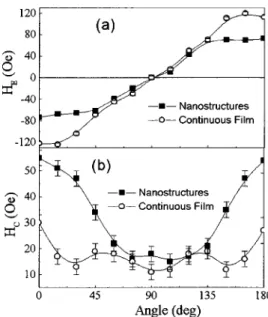
the continuous film兲 to 70 Oe 共in the nanostructures兲. The unidirectional character of exchange bias is revealed by the angular dependence of HE for the continuous film and the
nanostructures, shown in Fig. 2共a兲. The decrease of HE in
FM–AFM submicron dots has been sometimes reported in the literature.5,6,9,10 This effect is probably related to some constraints imposed by the reduced lateral dimensions of the nanostructures on the formation of domain walls in the AFM. It can be argued that the presence of AFM domain walls allows a small surplus of magnetization at the FM–AFM interface, which couples with the FM, resulting in the unidi-rectional anisotropy.3,18Taking into account the values of the magnetic stiffness for IrMn (AIrMn⬃10⫺11J/m3) and its magnetic anisotropy (KIrMn⬃1.8⫻105 J/m3), the domain wall width in IrMn, ␦IrMn, can be roughly estimated to be
␦IrMn⬃ (AIrMn/KIrMn)1/2⬃25 nm.19,20Hence, when the
lat-eral dimensions of the nanostructures become of about the same order of magnitude as the AFM domain wall width, it is likely that some AFM domain walls, instead of being able to completely form共i.e., 180° domain walls兲, they may just be partially developed inside the nanostructures. These par-tial AFM domain walls may be less effectively pinned during magnetization reversal than complete domain walls in con-tinuous FM–AFM films, thus leading to the observed de-crease of HE. In addition, a training effect was observed in
the nanostructures, i.e., the value of HE was found to
de-crease by about 15% in the dots during the first three hyster-esis loops, whereas no training effect was observed in the continuous film. Training effects are usually attributed to par-tial reorientation of AFM domain walls with each FM mag-netization reversal.1Since this effect could only be observed in the nanostructures, this seems to confirm that, indeed, AFM domain walls may become less effectively pinned when reducing lateral dimensions of FM–AFM systems.
Contrary to HE, the coercive field increases in the
nano-structures along the unidirectional direction. Figure 2共b兲 shows the angular dependence of the coercive field for the continuous film and the dots. It is noteworthy that the coer-cive field of the dots when the hysteresis loop is measured at 90° from the field cooling direction is just slightly larger than that for the continuous film. Actually, an enhancement of HC
is commonly observed in patterned FM elements due to shape anisotropy or to the role of the edges of the nanostruc-tures as barrier for the domain wall propagation.17This effect is mainly isotropic 共i.e., the same for 0° or 90°兲. However, the HC enhancement associated with FM–AFM exchange
coupling in the dots is somewhat more pronounced than that of the continuous film for angles deviating as much as 45° from the field cooling direction. Hence, in our case, the large
HC enhancement in the nanostructures seems to originate, at
least in part, from size effects on FM–AFM interactions. Indeed, if the domain walls in the AFM are less pinned than in the continuous film, the irreversibility associated with par-tial dragging of AFM spins during reversal of the FM in the dots can lead to the observed additional enhancement of HC
in the nanostructures. This result is particularly interesting since it can be used to enhance the magnetic stability of patterned media.
Exchange bias is known to typically vanish during heat-ing at a temperature denoted as blockheat-ing temperature, TB.
1
For single crystalline or relatively thick AFM layers, this temperature is usually close to the Ne´el temperature of the AFM, TN. However, in some cases, TB is much lower than
FIG. 1. Hysteresis loops of the continuous film and the array of dots, mea-sured at room temperature by longitudinal Kerr effect along the field cooling direction after cooling from T⫽450 K in the presence of a field HFC ⫽2.4 kOe. The inset shows the SEM image of the dots.
FIG. 2. Angular dependence of共a兲 the exchange bias field, HE, and共b兲 the
coercive field, HC, measured at room temperature, for the field-cooled array
of dots and the continuous
film.-4924 Appl. Phys. Lett., Vol. 84, No. 24, 14 June 2004 Baltzet al.
TN. This effect is particularly pronounced when either the
grain size of the AFM or the AFM layer thickness is rela-tively small.21–24In general, due to local variations in inter-face roughness or AFM crystallite sizes, a distribution of ‘‘local’’ blocking temperatures is encountered.1 A standard procedure to study the TB distribution is to progressively heat the sample to several temperatures, Theat⬍TB, and cool it in the presence of a field with opposite sign to the original cooling field.21,24Doing so, the magnitude of HE, measured at room temperature, progressively decreases and changes sign. The relative change in HE when cooling from two
suc-cessive temperatures gives an idea of the number of FM– AFM regions with local blocking temperatures comprised between the two given temperatures.
The dependence of HE, for the dots and the continuous
film, on the temperature from which the samples have been field cooled in the negative field is shown in Fig. 3. As ex-pected, HE decreases with temperature in both cases.
How-ever, for the nanostructures, HE is found to vanish at
THE⫽0⬃345 K, whereas THE⫽0⬃370 K for the continuous
film. It should be noted that, at THE⫽0, half of the FM-AFM
regions are coupled ‘‘positively’’ and half ‘‘negatively’’ or, in other words, half of the regions have local blocking tempera-tures above TH
E⫽0and half below. In addition, the
tempera-ture at which HE stabilizes after field cooling in a negative
field 共which corresponds to the maximum local blocking temperature兲, is found to be TB,max⬃400 K for the dots and
TB,max⬃430 K for the continuous film. Shown in the inset of
Fig. 3 is the derivative dHE/dTheat, which is typically used
to represent the blocking temperature distribution in FM– AFM exchange coupled materials.21The derivative indicates that, indeed, the blocking temperature distribution for the dots is shifted toward lower values. This reduction in TB
should be taken into account in the design of devices in the deep sub-100 nm range.
Usually, finite size effects on FM or AFM particles共or thin films兲 are only observed when their sizes 共or thickness兲 become very small 共i.e., a few nanometers兲. At these sizes, the particles tend to lose their magnetic order due to the increasing role of thermal energy with respect to the anisot-ropy energy.25 Reductions in the Curie and Ne´el tempera-tures have been experimentally reported26,27and theoretically
interpreted.28Our results seem to indicate that size effects on exchange bias start to appear at a lateral length scale some-what larger than that at which the Curie or Ne´el temperature in the FM or AFM counterparts would be expected to reduce.25–28This effect may be interpreted as being due to an increasing role of thermally induced unpinning of AFM do-main walls in the nanostructures. This hypothesis would be in agreement with the formation of partial domain walls in the FM–AFM dots, which could become less effectively pinned as temperature is increased.
This work was supported by the European Community through NEXBIAS Grant No. HPRN-CT-2002-00296. The authors acknowledge Stephane Auffret and Ursula Ebels for their discussions and technical assistance.
1For recent reviews on exchange bias, see J. Nogue´s and I. K. Schuller, J.
Magn. Magn. Mater. 192, 203共1999兲; A. E. Berkowitz and K. Takano,
ibid. 200, 552共1999兲; R. L. Stamps, J. Phys. D 33, R247 共2000兲; M. Kiwi,
J. Magn. Magn. Mater. 234, 584共2001兲.
2D. Mauri, H. C. Siegmann, P. S. Bagus, and E. Kay, J. Appl. Phys. 62,
3047共1987兲.
3
A. P. Malozemoff, Phys. Rev. B 35, 3679共1987兲.
4M. Kiwi, J. Mejı´a-Lo´pez, R. D. Portugal, and R. Ramı´rez, Europhys. Lett. 48, 573共1999兲.
5M. Fraune, U. Ru¨diger, G. Gu¨ntherodt, S. Cardoso, and P. Freitas, Appl.
Phys. Lett. 77, 3815共2000兲.
6J. Yu, A. D. Kent, and S. S. P. Parkin, J. Appl. Phys. 87, 5049共2000兲. 7Y. Shen, Y. Wu, H. Xie, K. Li, J. Qiu, and Z. Guo, J. Appl. Phys. 91, 8001
共2002兲. 8
A. Hoffman, M. Grimsditch, J. E. Pearson, J. Nogue´s, W. A. A. Macedo, and I. K. Schuller, Phys. Rev. B 67, 220406共2003兲.
9Z. B. Guo, K. B. Li, G. C. Han, Z. Y. Liu, P. Luo, and Y. H. Wu, J. Magn.
Magn. Mater. 251, 323共2002兲.
10E. Girgis, R. D. Portugal, H. Loosvelt, M. J. Van Bael, I. Gordon, M.
Malfait, K. Temst, C. Van Haesendonck, L. H. A. Leunissen, and R. Jonckheere, Phys. Rev. Lett. 91, 187202共2003兲.
11B. Dieny, V. S. Speriosu, S. S. P. Parkin, B. A. Gurney, D. R. Wilhoit, and
D. Mauri, Phys. Rev. B 43, 1297共1991兲.
12
K. Liu, J. Nogue´s, C. Leighton, H. Masuda, K. Nishio, I. V. Roshchin, and I. K. Schuller, Appl. Phys. Lett. 81, 4434共2002兲.
13V. Skumryev, S. Stoyanov, Y. Zhang, G. Hadjipanayis, D. Givord, and J.
Nogue´s, Nature共London兲 423, 850 共2003兲.
14S. Tehrani, J. M. Slaughter, M. Deherrera, B. N. Engel, N. D. Rizzo, J.
Slater, M. Durlam, R. W. Dave, J. Janesky, B. Butcher, K. Smith, and G. Grynkewich, Proc. IEEE 91, 703共2003兲.
15S. Landis, B. Rodmacq, B. Dieny, B. Dal’Zotto, S. Tedesco, and M.
Heitz-mann, Appl. Phys. Lett. 75, 2473共1999兲; S. Landis, B. Rodmacq, and B. Dieny, Phys. Rev. B 62, 12271共2000兲.
16
J. Sort, H. Glaczynska, U. Ebels, M. Giersig, J. Rybczynski, and B. Dieny, J. Appl. Phys.共in press兲.
17For a recent review on the fabrication and properties of magnetic
nano-structures, see: J. I. Martin, J. Nogue´s, K. Liu, J. L. Vicent, and I. K. Schuller, J. Magn. Magn. Mater. 256, 449共2003兲.
18
P. Milte´nyi, M. Gierlings, J. Keller, B. Beschoten, G. Gu¨ntherodt, U. Nowak, and K. D. Usadel, Phys. Rev. Lett. 84, 4224共2000兲.
19D. Suess, T. Schrefl, W. Scholz, J. V. Kim, R. L. Stamps, and J. Fidler,
IEEE Trans. Magn. 38, 2397共2002兲.
20
M. J. Carey, N. Smith, B. A. Gurney, J. R. Childress, and T. Lin, J. Appl. Phys. 89, 6579共2001兲.
21S. Soeya, S. Nakamura, T. Imagawa, and S. Narishige, J. Appl. Phys. 77,
5838共1995兲.
22
T. Ambrose and C. L. Chien, J. Appl. Phys. 83, 6822共1998兲.
23
A. J. Devasahayam and M. H. Kryder, J. Appl. Phys. 85, 5519共1999兲.
24C. Tsang and K. Lee, J. Appl. Phys. 53, 2605共1982兲.
25For a recent review on magnetic properties of fine particle systems, see: X.
Batlle and A. Labarta, J. Phys. D 35, R15共2002兲.
26
F. Huang, M. T. Kief, G. J. Mankey, and R. F. Willis, Phys. Rev. B 49, 3962共1994兲.
27F. Bødker and S. Mørup, Europhys. Lett. 52, 217共2000兲.
28W. H. Zhong, C. Q. Sun, B. K. Tay, S. Li, H. L. Bai, and E. Y. Jiang, J.
Phys.: Condens. Matter 14, L399共2002兲.
FIG. 3. Dependence of the exchange bias field, HE, on the temperature
(Theat) from which the dots and the continuous film, initially field cooled in HFC⫽2.4 kOe, have been field cooled in HFC⫽⫺2.4 kOe. All measure-ments have been performed at room temperature. Note that the lines are guides for the eye. Shown in the inset is the derivative dHE/dTheat.
4925
Appl. Phys. Lett., Vol. 84, No. 24, 14 June 2004 Baltzet al.