Design and Fabrication of Nanotweezers for
Nanomanipulation
By
Fardad A. Hashemi
B.S. University of California at Berkeley (1998)
M.S. Massachusetts Institute of Technology (2000)
Submitted to the Department of Mechanical Engineering
in partial fulfillment of the requirements for the degree of
OF TECHNOLOGY
Doctor of Philosophy in Mechanical Engineering
JU
N
1 6
2005
at the
at
LIBRARIES
MASSACHUSETTS INSTITUTE OF TECHNOLOGY
June,
2005
C2005 Massachusetts Institute of Technology. All rights reserved.
Author... ... e.... . . . ...
Department of Mechanical Engineering
18 May, 2005
Certified by... ...
... ...
...
Gang Chen
ofessor of Mechanical Engineering
Thesis Supervisor
A ccepted by ...
Lallit Anand
Professor of Mechanical Engineering
Design and Fabrication of Nanotweezers for Nanomanipulation
By
Fardad A. Hashemi
Submitted to the Department of Mechanical Engineering on 18 May, 2005
in partial fulfillment of the requirements for the degree of
Doctor of Philosophy in Mechanical Engineering
ABSTRACT
Experimentation and realization of new product concepts at the nanoscale present new challenges. Due to the diffraction limit of visible light it is not possible to see at this scale using optical microscopes. The Scanning Tunneling Microscope (STM) and the Atomic Force Microscope (AFM) are widely used tools for visualization at this scale and serve as the eyes into the nano-world. The ability to probe, manipulate, and construct at this scale is a continuing challenge that needs to be addressed. There are concurrent projects in both industry and academia to construct nanotweezers to serve as the hands and arms for nanomanipulation. Most such devices are not fabricated using completely batch processes and lack the consistency, feature definition, and ease of production required for general use. In this project, we propose a completely batch fabricated nanotweezer designed for compatibility with the AFM. We have developed a completely batch process for making overhanging, electrostatically actuated, compliant mechanism nanotweezers with nanoscale gripper motion resolution. The nanotweezer we tested requires lower actuation voltage and is more compliant than other similar grippers. It also has desired out of plane stiffness and resonance modes for operation with the AFM. We have also developed a batch process to fabricate self-aligned nanoscale tips with nanoscale spacing without the need for nanoscale lithography. The two processes are compatible and can be combined to batch fabricate consistent and practical nanotweezers for large scale use.
Thesis Supervisor: Gang Chen
ACKNOWLEDGMENTS
It is now near the end of the last part of my Ph.D. experience and I have a little time to reflect on this experience and the people who helped and taught me.
To my a dvisor Prof. Gang Chen I am most grateful for his advice and s upport during this project. His vision started this project and gave me a chance to work on a topic that I truly enjoyed. Through a unique combination of frankness and patience Gang has taught me a lot about his approach to problem solving and life in general. He always has our best interest in mind and I feel privileged to have worked in his group.
I have the deepest respect and admiration for Prof. Scott R. Manalis who agreed
to be on my committee and advised me throughout the project. Prof. Manalis's advice has always been dead on. I am privileged to have had the benefit of his experience and all the wrong paths it saved me from.
I decided to pursue the Ph.D. in part due to Prof. Alexander H. Slocum. His
enthusiasm for design and engineering is both contagious and addictive. I had to stay to learn more and let my mind stumble into and out of new hidden places yet to be discovered. I was so grateful to have the benefit of his advice and encouragement when he agreed to be on my committee. I am even more grateful for his constructive criticism.
I have been lucky to be in company of such good lab mates. Gang definitely knows how to pick the best of MIT. In particular, I want to thank Chris Dames for our many long hours of discussion. A lot of good ideas came from our discussions, and perhaps even more important, a lot of bad ideas were rightfully discarded as a result. His support has been invaluable.
I wanted to thank the wonderful people at MTL for their insight, patience, and
support. I have learned a lot from them. In particular, I want to thank Vicky Diadiuk for her kindness, advice, and understanding; Gwen Donahue for her immense knowledge of microfabrication which she was so willing to share; Kurt Boderick for his enthusiasm and instruction; Eric Lim for helping me better understand and fine tune processes; Paul Tierney for introducing me to the clean room and for his patient explanations; and Dennis Ward for his incredible understanding of the DRIE processes and for making things so much easier to accomplish.
I also wanted to thank Prof. Dennis M. Freeman for letting me use his laboratory
equipment and Shih-Chi Chen for teaching me how to use it. I was able to get a much better understanding of my devices from the data I obtained using this equipment.
As all mechanical engineering graduate students, I can not possibly thank Leslie Regan enough for taking care of us. She is our all knowing guardian. She is the first one we turn to when we need help and she always comes through for us.
I am thankful to my friend Kumaran for his relaxed intensity and support during
my quals; to my loving friend Merche, her husband, and their adorable daughter for their support and warmth; to Pouyan for our many escapades and conversations; to Reza for staying true to his principles; to Anjelica for her support over our many years of friendship and for calling me to make sure I was working on this thesis. To all of you many many thanks. I am indebted to my good friend Navid Sabbaghi for his wisdom and selflessness. My growth to this stage would not have been possible without his advice and mentoring. I am a better person as a result of our long friendship.
Finally, I would like to express my everlasting gratitude to my parents Fereidoon and Sohi Hashemi and my bother Farshid. They made many sacrifices for my education and well being. They taught me the value of dignity, character, and how to maintain balance in life. I will strive to follow their example as best as I can.
Contents
Chapter 1 Introduction... 21
1.1 Background ... 21
1.2 Prior W ork ... 23
1.3 M otivation... 25
1.4 N anotw eezer Requirem ents ... 25
1.4.1 K ey requirem ents ... 26 1.4.2 Target goals... 26 1.5 Thesis Overview ... 27 Chapter 2 D esign ... 29 2.1 D esign A rchitecture ... 29 2.2 Electrostatic A ctuators ... 33
2.2.1 Theory for electrostatic actuators... 33
2.2.2 Parallel plate electrostatic actuators... 35
2.2.3 Com bdrive electrostatic actuators... 37
2.2.4 Comparison of parallel plate and combdrive actuators... 39
2.3 M odeling of the Flexure Behavior... 42
Chapter 3 Fabrication ... 66
3.1 Pattern Combination/Multiplication Lithography... 66
3.2 D RIE Process ... 78
3.3 Surface Tension ... 80
3.5 Struct-v3 Process ... 83
3.5.1 Bum pers ... 89
3.6 Outcom e of Fabrication ... 91
Chapter 4 D evice Testing ... 93
4.1 Experim ental Setup... 93
4.2 Analysis and Explanation of Results ... 97
Chapter 5 N anocut Process... 104
5.1 Process Flow ... 104
5.2 Process Results... 108
5.3 Com bination of N anocut and Struct-v3 processes... 114
5.4 Other Applications of N anocut ... 116
Chapter 6 Future W ork and Conclusion... 119
6.1 Future W ork and Considerations ... 119
6.1.1 Robust design paradigm ... 119
6.1.2 Sensing tip sam ple interactions... 123
6.2 Lessons Learned... 130
6.2.1 N anoscale tips ... 130
6.2.2 Process flow developm ent ... 131
6.2.3 Sub-process debugging ... 132
List of Figures
Figure 2-1. Schematic showing how a SOI wafer is used to fabricate the nanotweezers. Nanotweezers are fabricated in the device layer. Parts of the substrate and oxide layer are removed to create overhanging structures...30 Figure 2-2. Schematic showing the function of an AFM probe. An optical lever
consisting of a laser beam that reflects of the back of the cantilever and into the photodiode detector measures probe deflection. This deflection is indicative of the force interaction between the tip and the sample...31 Figure 2-3. Schematic showing the in-plane design of the overhanging nanotweezer
structure. The two arms on the side each have a flexure mechanism for translation and combdrive for actuation. ... 32
Figure 2-4. Schematic of a general electrostatic actuator. Force F is the force exerted on the actuator. Coordinate x is the position of the moving electrode relative to the fixed electrode on the right. ... 33
Figure 2-5. Schematic of a parallel plate electrostatic actuator pulling against a spring of constant k... 36
Figure 2-6. SEM of a combdrive actuator showing the interdigitated teeth...38 Figure 2-7. Schematic of a combdrive electrostatic actuator. Only one comb tooth is
shown for simplicity. In practice many comb teeth are used (dimmed lines). x0 is the amount of interdigitation as fabricated. ... 38
Figure 2-9. Diagram indicating annotation for each beam comprising the nanotweezers arm flexure mechanism. Color coordination of the annotation indicates a symmetric set: blue for set A, red for set B, and green for set C...43 Figure 2-10. Diagram highlighting the smaller junctions that connect beam set A with
B ... . . 4 5
Figure 2-11. Schematic showing positive force and moment notation for an elemental beam section... 46 Figure 2-12. Diagram highlighting the half hammock beam set C. This part of the
flexure mechanism forms a hammock type flexure and can be analyzed independent of the other beam s ... 47 Figure 2-13. Force and moment diagram for beam set C. Insert on the top left corner
indicates the section of the flexure mechanism that is depicted in the diagram. This section is the larger junction that connects beam set B with
C. The x coordinate system originates from the larger junction. The
positive direction for deflections of the beam is horizontal and to the left...48 Figure 2-14. Force and moment diagram for beam set A. Insert on the top left corner
indicates the section of the flexure mechanism that is depicted in the diagram. This is the anchor section of flexure mechanism that connects beam set A to the substrate. The x coordinate system originates from the anchor points. The positive direction for deflections of the beam is horizontal and to the left. ... 51
Figure 2-15. Force and moment diagram for junction of beam 1 and 2. This is one of the smaller junctions that connects beam set A with B. This junction is
the one on the left indicated in Figure 2-10. The x coordinates point in opposite directions. The positive direction for deflections of the beam is horizontal and to the left. ... 52
Figure 2-16. Force and moment diagram for the junction of beam 4 and 5. This is one of the smaller junctions that connects beam set A with B. This junction is the one on the right indicated in Figure 2-10. The x coordinates point in opposite directions. The positive direction for deflections of the beam is horizontal and to the left. ... 53
Figure 2-17. Force and moment diagram for the larger junction connecting beam set B with C. Insert on the top left corner indicates the section of the flexure mechanism that is depicted in the diagram. The loading from beam set C on the junction is represented as force moment pair. The positive direction for deflections of the beam is horizontal and to the left. ... 55
Figure 2-18. Schematic of kinematic constraints for the beam set junctions. Using the axially rigid beam assumption, any rotation of the larger junction (of length yL) must be completely accommodated for by consequent rotations of the small junctions (of length yo)... 57
Figure 2-19. FEA model of the left nanotweezer arm subjected to an out of plane force at the tip. The model shows exaggerated deflection. This is a 1000x model where the color bar shows displacement in units of mm corresponding to units of pm in real life. A model force of 0.15 N is applied corresponding to real life force of 1.5x 10⁻⁷ N...62
Figure 2-20. FEA diagram showing the 6th resonance mode of vibration of the
nanotweezer arm. Deformation has been exaggerated for visualization. ... 64 Figure 2-21. FEA diagram showing the 7th resonance mode of vibration of the
nanotweezer arm. Deformation has been exaggerated for visualization. ... 64 Figure 3-1. Diagram showing the effect of shuttering and offset with a stepper
lithography tool on the wafer pattern. The top two diagrams show the area of the reticle that is shuttered down. The lower left diagram shows the resulting exposed pattern on the wafer. The lower right diagram shows the same pattern offset to the center of the die. Offset is achieved
by moving the wafer underneath the reticle...68
Figure 3-2. Diagram showing the shuttering of two regions of the reticle to be combined for exposure on the wafer. The two patterns, which are disjoint on the reticle, will be offset during exposure to form a connected pattern on the w afer space... 69
Figure 3-3. :Diagram showing pattern combination of two disk patterns, a) shows the commonly expected resulting pattern that is incorrect, b) shows the actual pattern resulting from the combination of the two disks, c) shows what patterns need to be combined to from the desired pattern of a)...70 Figure 3-4. Diagram showing how the pattern in the converging zone of the contact
pads (shown in black cross-hatch) combines with the nanotweezer pattern (shown in red cross-hatch) ... 72
Figure 3-5. Diagram showing potential pattern errors that can be caused by misalignments and ways to avoid them. a) shows the spikes caused by
horizontal misalignment, b) shows how to avoid the spikes by use of a bridge segment, c) shows effect of horizontal misalignment on the bridge segment, and d) shows effect of vertical misalignment on the bridge segm ent ... . . 73
Figure 3-6. Diagram showing how encompassing bridge segments can be used to avoid narrowing of bridge segments due to misalignment of the patterns. ..74 Figure 3-7. Diagram demonstrating the use of tangential circular bridge segments to
prevent sharp concave and convex corners caused by misalignment of the patterns, a) perfectly aligned, b) horizontally misaligned, c) vertically m isaligned ... 76
Figure 3-8. Diagram showing the use tangential encompassing circular bridge segments. This combined approach both preserves minimum bridge width and avoids sharp concave and convex corners despite misalignment of the patterns... 77
Figure 3-9. SEM photos showing the result of pattern combination/multiplication lithography in practice, a) shows how the pattern from the large contact pads seamlessly converges down to the contact lines leading to the nanotweezer, b) is a magnified view of the intersection region showing a small step caused by the misalignment of the two patterns circled in red....78 Figure 3-10. SEM photo of structure formed by the FARDAD DRIE process showing
Figure 3-11. Close-up SEM photo of structures showing effect of surface tension on the structures. The slender beams have permanently adhered to each other and the device is destroyed ... 81
Figure 3-12. 2-D Diagram of the entire process flow. The left column (steps 1-4) shows the patterning and bracing of the device layer. The middle column (steps 5-8) shows the mounting of the SOI water and subsequent BOX layer removal and die separation. The right column (step 9) is the final ashing step... 83
Figure 3-13. Process flow diagram for nanotweezers structures at the completion of step 2 (post DRIE). Insert on the right shows a perspective view of a representative 3 x 3 die section of the wafer. ... 84
Figure 3-14. Process flow diagram for nanotweezers structures at the completion of step 4 (post PR brace). Insert on the right shows a perspective view of a representative 3 x 3 die section of the wafer. ... 85
Figure 3-15. Process flow diagram showing the device wafer mounted to a mount wafer a). The mount wafer has special pillars and channels surface micromachined into its interface surface with the device wafer. The locations of these pillars and channels relative to the device wafers are shown in a see through diagram b). ... 86
Figure 3-16. Process flow diagram for nanotweezers structures after step 8 (post backside die release). Insert on the right shows a perspective view of a representative 3 x 3 die section of the wafer. ... 88
Figure 3-17. Process flow diagram for nanotweezers structures at the completion of step 9 (post dry dismount). Insert on the right shows a perspective view of a representative 3 x 3 die section of the wafer. At this point the individual dies are no longer stuck to the mount wafer and can be
extracted for use... 89
Figure 3-18. Optical microscope photo of the wafer after the back side DRIE etch (step 7). The photo shows the nanotweezer section and the contact lines that are converging i n. Bumper s tructure t hat s urround t he n anotweezer a re surface micromachined in the device layer to prevent cracks from propagating through the device... 90
Figure 3-19. SEM photos of the nanotweezers structures after extraction from the process. Insert on top corner of the picture on the right shows a magnified view of the tips region... 91
Figure 3-20. Close-up top view SEM photo of the nanotweezer flexure mechanism showing beam anchor points... 92
Figure 4-1. Photograph of experimental setup... 94
Figure 4-2. SEM photo of the nanotweezers in the closed position ... 96
Figure 4-3. Close-up SEM photo of the nanotweezers' tips in the open and closed positions ... . 96
Figure 4-4. Graph showing measured vs. calculated actuation data...97
Figure 4-5. Amplitude plot for in-plane frequency response of the nanotweezers...98
Figure 4-7. Diagram showing the effect of the footing from the DRIE etch on the beam
cross-section ... 99
Figure 4-8. SEM photo showing the effect of the footing from the DRIE etch on the structure. The effect is visible underneath the structure where the BOX layer w as, prior to rem oval...100
Figure 4-9. Graph showing measured vs. calculated actuation data. The new calculated data accounts for structural deviations caused by footing by incorporation of an effective beam thickness and combdrive gap. In this case, effective parameters were optimized to match deflection data...101
Figure 4-10. Graph showing measured vs. calculated actuation data. The new calculated data accounts for structural deviations caused by footing by incorporation of an effective beam thickness and combdrive gap. In this case, effective parameters were optimized to match in-plane frequency resp on se...102
Figure 5-1. Process flow diagram for the Nanocut process ... 105
Figure 5-2. SEM photos of features created using the Nanocut process. On the left is a view of a pyramidal wall created by a nitride line mask. On the right is a cross-section view of a similar pyramidal wall...107
Figure 5-3. Close-up cross-section SEM photos of a pyramidal wall created using the N anocut process...108
Figure 5-4. SEM photo of experimental results for the Nanocut process...108
Figure 5-5. Graph of oxidation thickness vs. time for the thermal oxidation process...109
Figure Figure
Figure
Figure
Figure
5-7. Schematic of the combined Nanocut and Struct-v3 processes...115 5-8. SEM photos of thin walls micromachined into Si using the Nanocut
p ro cess...1 17
5-9. SEM photos showing the application of the Nanocut process to rings
fabricated for M etamaterials applications...118
5-10. SEM photos showing an array of apertures created using the Nanocut
p ro cess...1 18
6-1. Diagram showing the attachment of an external flexure based grating to
the existing nanotweezer arm. The grating flexure would be designed to be much more compliant than the arm flexure. ... 127
6-2. Plots showing normalized intensity of reflection of a grating as a
functional of angle a), with increased number of grating lines b), with increased spacing between the grating lines c)...128
6-3. Plots showing normalized intensity of reflection of a flexure arm grating
as a functional of angle. Blue plot corresponds to the relaxed state. Red plot corresponds to the fully extended state...129 Figure
List of Tables
Table 1-1. Summary of design requirements... 28
Table 2-1. Table showing characteristics of the combdrive actuator. A range of 2 tm is required of each arm to close the 4 pm gap of the nanotweezers...61
Table 2-2. Table showing various displacement results and subsequent spring constants derived from FEA model. All spring constants are measured at the tip...63
Table 3-1. Table of parameters for "FARDAD" DRIE etch recipe...80
Table 5-1. Table of starting oxide thickness for each wafer...110
Table 5-2. Table of oxide thickness for each wafer post nitride etch...110
Table 5-3. Table of oxide thickness for each wafer post DRIE etch ... 111
Chapter
1
Introduction
1.1 Background
The benefits of higher density, smaller electronic devices, lower power consumption, and the ability to engineer new materials have fueled technological advances for working at continuously smaller length scales. The progress from microscale to nanoscale, however, transitions below the wavelength of visible light and presents its unique challenges. Due to the diffraction limit of visible light it is not possible to see at this scale using optical microscopy. A new set of tools are needed for imaging and manipulation at this scale.
To address this, in 1981 IBM researchers, Bining and Rohrer, developed the scanning tunneling microscope (STM). In similar manner to a stylus profiler', the STM scans a sample using tunneling current between an ultra sharp tip and the sample to generate three dimensional surface topography.2 The STM provides resolution down to individual atoms but can only image conducting samples. To address this limitation, in
1986 Binning, Quate, and Geber invented the atomic force microscope (AFM). This
microscope scans similar to the STM but uses force interactions of the sharp tip, instead of tunneling current, to generate topography.3 The AFM measures deflections of a very flexible cantilever supporting the tip as an indication of the tip-sample force interaction. The original setup of the AFM used a STM probe to measure deflections of the AFM via tunneling current between the two. Today most commonly, a laser beam reflected off of
the cantilever to a photodiode is used as an optical lever system to measure deflections of the cantilever. Other methods have been developed since to improve AFM performance. Two such examples include measuring diffracted mode intensity off of a grating created
by interdigitated fingers attached to the cantilevers4 and the use of cantilevers with
integrated piezoresistive sensors and piezoelectric actuators.5 New methods to enhance and build upon the capabilities of AFM are still being developed. The AFM is one of the most commonly used tools for visualization at nanoscale and serves as the primary eyes into the nano-world.
The ability to probe, manipulate, and construct at this scale has been even more challenging. There has been some success at nanomanipulation using the AFM probe as means to push and pull objects around on the sample.6 A novel example of this is by
Superfine and his group who connected a haptic interface to the AFM7 to assist in
nanomanipulation. Their setup allowed the user to feel the force for the tip on the sample in real time. The haptic interface allowed for more precise manipulation of the sample. Using Superfine's nanoManipulator scientists were able to manipulate and extract mechanical properties for viruses8, DNA', and carbon nanotubes10 and investigate friction at the molecular level." Despite this and other advances, as of yet, there are no practical tools that can be used to grip, pick, and place objects for general experimental setup and realization of new product concepts. The arms and hands to grip and pick up objects at the nanoscale are a much needed goal still under development. This thesis is an attempt to add gripping manipulation functions to the AFM, through the development of batch fabricated nanotweezers.
1.2 Prior Work
Perhaps the earliest microfabricated gripper was made at UC Berkeley'2 in 1992.
These were overhanging devices able to access and pick up micro-size objects. They did not have nanoscale tips and were not intended to pick up smaller objects. However, the microgrippers were well suited for general use and quantity production because they were completely batch fabricated.
In 1999, Lieber's group of Harvard university demonstrated one of the first proofs of concept of a nanotweezer made out of carbon nanotubes.1 3 Their nanotweezers were
constructed by depositing two electrically independent gold electrodes onto a micropipette and then attaching a carbon nanotube to each electrode. When the two carbon nano-tubes were biased electrically with respect to each other, they attracted each other and would close similar to tweezers. Although the two arms were separated by 2pm, each one was only 50nm in diameter making it more suitable for interacting with nanoscale objects than the microgrippers. In addition, Lieber's nanotweezers required only 8.3V to fully close compared to 45V for the microgrippers. However, Lieber's devices were individually fabricated and not suitable for large scale use. Lieber and his group were able to pick up 500-nm polystyrene clusters using a light microscope for visualization. They also successfully used to pick up and electrically probe GaAs nanowires. The results were consistent with theoretical predictions.
An improved version Lieber's nanotube-based nanotweezers was made by Seiji Akita and Yoshikazu Nakayama of Osaka Prefecture University who fabricated nanotweezers by attaching carbon nanotubes to an AFM tip.14 The AFM tip was first coated with a conducting Ti/Pt film that contacted larger Al contact lines. This film was
then c ut into two electrically independent s ections u sing a G a i on b earn. T hey u sed a specially designed SEM with three movable stages to position the nanotubes on each of the two coated regions of the tip. Finally e-beam contamination deposition was used to deposit an amorphous carbon film on the contact region of the tubes with the tip to secure them. While similar in function to Lieber's nanotweezers, these were created with use with an AFM in mind.
In addition, Boggild and his group from the Technical University of Denmark constructed a different type of nanotweezers by first batch microfabricating metal coated silicon oxide arms, and then individually growing tips at the end of the arms using focus electron beam contamination growth.1 5 Boggild's nanotweezers provided three major
improvements. First, his nanotweezers were at least partially batch fabricated making them easier to produce for large scale use. Second, these nanotweezers' arms could be closed without having to bias the tips with respect to each other. Finally, unlike the micro spaced nanotube nanotweezers, his deposited tips could be made with a gap of only 25nm.
1.3 Motivation
The previously mentioned nanotweezer projects prove the vision and concept but can be improved upon in their fabrication and design. The nanotweezers mentioned are not suitable for general large scale use since they are not readily producible using a batch process. In addition, due to limitations in their construction it is not possible to define a guided direction of motion and constrain compliance along specific directions. As with macroscale applications, it will be difficult to specifically select a single object within tight confines and pick it up with tweezers with that are equally compliant in many directions. In contrast to the nanotweezers, Kim's microgripper is an example of design intent resulting in a mass producible device with well defined features and performance optimized for tweezing applications. Similarly, for the full promise of nanotweezers to be exploited a practical way to manufacture them with guided motion and constrained compliance, and the ability to have better control of feature definition are necessary. Given the limitations of nanoscale patterning and fabrication, it is difficult to match Kim's level of feature definition with nanoscale fabrication. However, through careful re-consideration of required characteristics, alternate, more practical, and more controllable methods of achieving them is possible.
1.4 Nanotweezer Requirements
The objective of this project is to create a nanotweezer that combines the best advantages of the prior art nanotweezers into one that can be readily fabricated and optimized for tweezing. There are some key requirements that are critical to achieve this
objective and to the function of the devices for nanomanipulation. There are also non-critical target goals, which if possible, will greatly enhance the utility and versatility of a nanotweezer.
1.4.1 Key requirements
The first key requirement, which is also the motivation behind this project, is to be able to make functional nanotweezers using a completely batch process. Batch fabrication provides for both consistency and ease of production, both of which are necessary for large scale use and research utility. Second, for further increased research utility, the nanotweezers have to be compatible for use with AFM, as it is the primary visualization tool at this scale. The ultimate vision is to use the same device to both image and manipulate in an AFM. Nanoscale tips are also required both to function as an AFM tip and to be able to interact and access nanoscale objects with nanoscale spacing. Finally, nanoscale motion of the arms with constrained directions of compliance is required to be able to select and accurately grip the desired object based on the image provided by the AFM.
1.4.2 Target goals
In order to successfully pick up small aspect ratio nanoscale objects, such as spheres, it is necessary for the nanotweezers tips to meet at a point when they close. This can be achieved if either the tips maintain alignment as they close or if they can be fabricated in the closed state with a nanoscale gap that is then actuated open. In order to increase the chance of success, both nanoscale alignment of the tips as they close, and the
ability to fabricate tips with a nanoscale gap are target goals. In practice, however, either of the latter may be sufficient.
Another target goal is to create nanotweezers arms that are as compliant as possible in their intended axes of motion. Ideally, they can be fabricated with a spring constant within the range of contact mode AFM cantilevers, which is 0.05-iN/m. Although this is not a strict requirement, it will allow more compliant objects to be picked up without risk of damage and or the need to sense tip position. For a detailed analysis please see section 6.1.2.
Finally, it is desirable for the nanotweezers to require very low drive voltage to fully close. This would reduce the risk of electrical damage to the sample and is a feature that other projects like that of Lieber have emphasized with regard to their device. Table
1-1 summarizes these requirements and goals.
1.5 Thesis Overview
In this project, it is shown that overhanging structures with well defined guided nanoscale motion, desired in-plane compliance, low actuation voltage, and single pitch nanoscale features are possible using a completely batch process. The following sections will layout the design architecture, and subsequent detailed design and analysis of a proposed nanotweezer. Next, a process for fabricating this structure is detailed including the outcome of the fabrication. Actuation and frequency response results for the nanotweezer structure are presented along with justification for deviations from predicted results. Finally, a novel process for batch fabricating nanoscale, nanospaced tips using microscale lithography is illustrated and characterized. The proposed combination of the
two compatible processes can yield the desired final form of the nanotweezers. For the sake of presentation this thesis is centered on one specific nanotweezer design. However, the scope of project goes beyond this case example. The focus of this project is not to make one specific nanotweezer work but rather use a few specific designs as case studies to develop a general framework for the design and fabrication of nanotweezers of certain useful type. For other designs have been fabricated and tested using this general framework e-mail fardad@alum.mit.edu. The contributions of this work are its various innovations in design and fabrication approach that bring rigorous control of feature definition and ease of production into the execution of a useful type nanotweezers for nanomanipulation.
Key Requirements Justification
Complete Batch Fabrication -ese osoutin
-Ability to image and manipulate
Compatibility with AFM need for calibration to another probe tip
-Ability to scan as an AFM probe Nanoscale sharp tips -Ability to access within nanoscale
Confines
Nanoscale motion control of the tips -Ability to accurately select and grip an object from within tight confines -Ability to accurately select and grip Constrained compliance an object from within tight confines
Target Goals Justification
Nanoscale alignment of the tips as -Ability to pick small aspect ratio they close Objects
Nanoscale tip separation (gap) -Ability to pick small aspect ratioObjects -Ability to grip compliant objects without Highly compliant structures closed loop control of the tips position
-Reduce risk of electrical damage to sample Low actuation voltage -Reduce the need to place a matching bias
voltage on the sample
Chapter 2 Design
The proposed nanotweezer for this project consists of two arms that can move and close a t t he t ip r egion t o g rip o bjects. T his i s a ssumed t o b e t he b asic definition o f a tweezer. In this regard, the proposed nanotweezer is no different than that of Lieber, Boggild, or macroscale tweezers. However, its design architecture has b een defined to
satisfy a different set of requirements as detailed in sections 1.4 and 1.5.
2.1 Design Architecture
The design architecture dictates both the general physical layout of the device and also the fabrication approach. The two are interconnected due to constraints in microfabrication and microassmbly. The architecture determines what technical challenges need to be solved in order to meet the requirements and goals.
To meet the requirement for complete batch production, the entire fabrication, including that of the nanoscale sharp tips, is designed u sing s tandard microfabrication processes and microscale lithography. Although nanoscale lithography is available in some industrial clean rooms, it is not available at MIT's Microsystems Technology Laboratory or other similar educational facilities and is not used for this reason. Since gripping or tweezing action involves in plane motions, the SOI wafer is adopted as the fabrication medium. This medium is widely used in MEMS applications. As a result, there is a large number of mature microfabrication processes already developed for its use. As shown in Figure 2-1, SOI wafers consist of a device layer used for the
nanotweezer structure and tips, a sacrificial oxide layer that is removed to release and mobilize the structures, and a large substrate layer that serves as a handle.
Si device layer
Burried oxide
Si substrate
Figure 2-1. Schematic showing how a SOI wafer is used to fabricate the nanotweezers. Nanotweezers are
fabricated in the device layer. Parts of the substrate and oxide layer are removed to create overhanging structures.
As shown in Figure 2-2, an AFM probe is an overhanging structure that accesses the sample from the one side while the AFM laser accesses it from the other to measure its deflection. To be used as an AFM probe, the nanotweezers must also be overhanging protruding structures with sharp tips that can be accessed from both the top and bottom. The handle section of the SOI is removed as shown in Figure 2-1 to give access from the bottom. In addition, just like AFM probes the nanotweezers are designed to have adequate out of plane compliance to be able to scan over samples without damaging them. The goal is to have an out of plane spring constant within the range of 0.3-iN/m, for contact mode probes. Out of plane compliance and resonance modes of the nanotweezers, which are necessary for measuring tip sample force interactions, are achieved by adjusting the device layer thickness and the design of the in-plane structure.
A batch process is developed to achieve sharp tips with nanoscale spacing at the head of
Detector AM Laser
antilever
Tip
Sample
Figure 2-2. Schematic showing the function of an AFM probe. An optical lever consisting of a laser beam
that reflects of the back of the cantilever and into the photodiode detector measures probe deflection. This deflection is indicative of the force interaction between the tip and the sample.
For the in-plane motion of the nanotweezer arms a flexure mechanism is used. A flexure mechanism allows for guided motion between two objects via elastic deformation of it structure. Flexure mechanisms are often used in place of sliding guides, rails, and bearings in applications that require high precision and small range of motion. Since they do not have sliding components they do not suffer from sticktion or backlash and provide good repeatability within their elastic region of operation. If designed properly, flexure mechanism can selectively constrain compliance in specified directions. In general they are easier to produce than rails and bearings. The latter is particularly true in MEMS applications due to limitations of microfabrication and assembly of microscale objects. Figure 2-3 shows the in-plane layout of the nanotweezers design. The arms, located on the right and left, each have a dedicated flexure mechanism. The mechanism serves two purposes: to allow for guided motion; and act as a linear spring to resist the force of the actuator. Each arm also has an electrostatic actuator that pulls it towards the center electrode. Force from the actuator pulling against the linear flexure spring allows for the
predictable motion. The force of the actuator is matched to the stiffness of the flexure mechanism to allow nanoscale resolution in motion.
Figure 2-3. Schematic showing the in-plane design of the overhanging nanotweezer structure. The two
arms on the side each have aflexure mechanism for translation and combdrive for actuation.
Electrostatic actuators are used to provide a well controlled force to pull the arms inward. They were chosen mainly for their simplicity. Unlike piezo and magnetic actuators, electrostatic actuators are generally monolithic planar devices that can be fabricated out of the same conducting Si as the rest of the nanotweezers. They provide force as a repeatable function of voltage. The characteristic of this function and the sensitivity of output force to the input voltage can be customized via modifications of the actuator geometry. Through proper design and matching of the actuator and the flexure mechanism pair, highly compliant arms with nanoscale resolution in motion can be achieved.
2.2
Electrostatic Actuators
Electrostatic actuators convert electrical energy to mechanical work. They are often used in MEMS applications for their convenience. In most application, electrostatic actuators are used to generate planar motion.
2.2.1 Theory for electrostatic actuators
Figure 2-4 shows a simplified generic electrostatic actuator. In this notation the force F exerted on the actuator and x are in the direction that pulls the two electrodes apart.
Figure 2-4. Schematic of a general electrostatic actuator. Force F is the force exerted on the actuator. Coordinate x is the position of the moving electrode relative to the fixed electrode on the right.
Electrostatic actuators are two port systems with two degrees of freedom and
require two of the variables F, x, V, or q (the charge on stored on the plates) to describe
their state. Both mechanical and electrical work can be done on these systems to increase their energy.
Using the following constitutive relation,
V = q (constitutive relation)
C(x)
the energy of the system can be evaluated and expressed as,
E C(x)V2
2
(2-2)
(2-3)
Using the latter expressions, the force of the actuator, per the notation in Figure 2-4, can be expressed as,
F = d (general
force
expression) (2-4)2 dx
The above equation can also be re-evaluated and expressed as,
dE
dx
This suggests that positive mechanical work done on the actuator reduces its energy. While pulling with a force F in the direction of x does positive mechanical work on the actuator, it forces the actuator to do twice that much work out of its electrical port
thus reducing its energy. This is a consequence of the constitutive relation governing the electrical port and the energy balance equation is still satisfied.
F+V 2d_ C(x)V2 V2 dC
dx dx 2 2 dx
2.2.2 Parallel plate electrostatic actuators
Parallel plate actuators consist of two parallel plate electrodes that can move with respect to each other just as shown in Figure 2-4. Relative motion of the electrodes changes the capacitor gap and hence produces a dC/dx. As before, the general equation for force holds.
F V 2 dC
2 dx
where,
C(x) =
x (2-5)
and A is the area of the parallel plates.
Akt V2
As the above equation indicates, parallel plate actuators are nonlinear with motions in x and exert a force that is both a function of x and voltage.
2.2.2.1 Pull in
When connected to a linear spring (Figure 2-5), the nonlinear behavior of parallel plate actuators makes them prone to what is called "pull in".
Figure 2-5. Schematic of a parallel plate electrostatic actuator pulling against a spring of constant k.
Given an initial relaxed-state gap of x=g, the following is the force balance condition for such an actuator spring system.
k(g - A)= 2 (force balance) (2-7)
2x'
Pull in occurs within the range where a perturbation & from equilibrium in x cause a larger perturbation in the actuator force than it does in the spring force.
d (AV2 )9 x
dx 2x'
In this unstable region the actuator plates, if perturbed open, will swing open into the stable region and re-approach to equilibrium. If perturbed closed they will slam shut, which is the inevitable result oft his instability. The system transitions to the unstable range when,
(2-8)
3 = k x3
Simultaneous evaluation with the force balance equation results in
2g,
3 (2-9)
Therefore, the nonlinear behavior of parallel plate actuators limits their stable range of operation to within one third of the starting gap as fabricated. Not all electrostatic actuators suffer from this instability. In comparison combdrive actuators achieve a constant dC/dx with position due to their design.
2.2.3 Combdrive electrostatic actuators
Combdrive actuators consist of two electrodes with interdigitated teeth as shown in the SEM photo in Figure 2-6. They are widely used in MEMS applications to generate
in-plane and out of plane motion'6. Unlike parallel plate parallel plate actuators, relative motion of the electrodes causes a change in the capacitor area and hence produces a constant dC/dx. Capacitor gap g, shown in Figure 2-7, does not change with x.
Figure 2-6. SEM of a combdrive actuator showing the interdigitated teeth
F
x
111
Figure 2-7. Schematic of a combdrive electrostatic actuator. Only one comb tooth is shown for simplicity. In practice many comb teeth are used (dimmed lines). x, is the amount of interdigitation as fabricated.
As before, the general equation for force holds.
2 dx
Cx) = 2ntxokc0 2ntxke0 (2-10)
g g
where n is the number of comb teeth, t is the thickness of the device layer out of the page,
g is the gap between the combdrive teeth, and x, is the amount of interdigitation at the
relaxed-state. Please refer to Figure 2-7. Combdrive actuators are linear, in fact, constant, with x and exert a constant force that is function of voltage.
F = n V2=cnst V2 (2-11)
g
2.2.4 Comparison of parallel plate and combdrive actuators
Parallel plate and combdrive actuators are both widely used in MEMS applications. Each has its own advantages and disadvantages. The primary difference is that combdrive actuators exert a linear force with respect to displacement while parallel plate actuators are highly nonlinear. It can be shown, however, that given the same feature fabrication resolution and device dimensions, parallel plate actuators can exerttwice the force of combdrive actuators for the same drive voltage. Given a device thickness of t and width w the force per voltage applied for parallel plate actuators is:
F= k
(2-12)
V2 2x2
where w is the width of the plate.
For a given w, the minimum x will achieve the largest force for applied voltage. Setting this to the minimum fabrication resolution r0 will yield the following equation.
F = ktwe
V2 2r2
The force per applied voltage for the combdrive is given by:
F = nktcO (2-13)
v2
where g is the gap between the combdrive teeth and n is the number of teeth.
Similarly for combdrive actuators the minimum g set to the minimum fabrication resolution r, and t he m aximum n w ill yield t he largest force p er a pplied v oltage. The maximum n can be achieved by setting the width and gap of the combdrive teeth to smallest possible dimension of ro, thus packing the most number of teeth in a given width
give the maximum force per voltage attainable with each actuator given the same size and fabrication constraints.
Fp~t (1a< )w bomb (16e_) w
VpIae 2 r comb )r 4 r
The parallel plate actuators can generate twice the force per voltage of that of the combdrives. However, combdrive actuators are linear and have longer range of motion. Since in this application linear performance and range are both important, the combdrive actuator is chosen over the parallel plate despite its lack of relative compactness and strength.
The dimensions of the combdrive, such as number of comb teeth and the gap between the comb teeth are designed to achieve a desired strength vs. drive voltage. The strength of the combdrive is designed to match the stiffness of the flexure mechanism it is pulling against. Please refer to end of the flexure design section 2.3 and Table 2-1 on page 61 for these values and justification. One consideration is that the actuator not be too strong so that small resolution in motion vs. voltage can be achieved. Yet the actuator must be strong enough to fully close the arms within a specified voltage range. Since low actuation voltage is target goal of this design, a drive voltage of approximately 25 V to fully close the nanotweezers is chosen as a target starting point for the preliminary design. This value is roughly half way between that of Lieber's nanotweezers (8.3V), which is ideally achievable, and Kim's microgrippers (45V), which is likely to be achievable. Given the test results from this design, which are discussed in section Chapter
4, it is fortunately possible to decrease the required drive voltage even further in future generations.
2.3 Modeling of the Flexure Behavior
In addition to serving as a linear spring for the actuator to pull against, flexure mechanisms allow for guided motion between two objects with constrained directions of compliance. A properly designed flexure will guide motion along a single intended direction while constraining it in all others. A hammock flexure such as the one shown in Figure 2-8 is commonly used. It allows translation in the x direction of the center piece. Hammock type flexures are used because they do a good job of constraining any motion but translation along the x direction.
Figure 2-8. Schematic of a typical hammock flexure.
In an earlier design, the flexure for the nanotweezer arm was also made of a single half hammock flexure equivalent to the lower half of the one shown in Figure 2-8. The
t,
YO I1I
F
4x
:E-x
Figure 2-14. Force and moment diagram for beam set A. Insert on the top left corner indicates the section
of the flexure mechanism that is depicted in the diagram. This is the anchor section offlexure mechanism that connects beam set A to the substrate. The x coordinate system originates from the anchor points. The positive direction for deflections of the beam is horizontal and to the left.
The force and moment diagram for the smaller junction that connects beam #1 with beam #2 is shown in Figure 2-15. For this junction,
ZFHorizontal =1 (La V2(O)=O
V(La )= A, =V2(0)= A2
A, =A 2
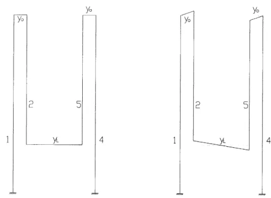
Beam #1 and beam #4 form the first, grounded symmetric set, set A. Beam #2 and beam
#5 form the second, floating symmetric set, set B. Beam #3 and beam #6 form the final, symmetric set C that connects to the actuator. Beam #2 is mounted in series to beam #1 and similarly beam #5 is mounted in series to beam #4. Beam set C is a half hammock flexure that is mounted in series to the rest of the mechanism at the junction where beam #2 and beam #5 come together. This junction from here on is referred to as the larger junction. Under the approximation of axially rigid beams, hammock type flexures such as the one in Figure 2-8 and beam set C, do not allow relative rotation between their two ends and incorporate a zero rotation boundary condition for both. It is important to note that the beam sets A and B, however, are not half hammock flexures. The reason is that the junctions (circled in red in Figure 2-10) that connect beam set A with B, from here on referred to as the smaller junctions, are free to rotate and hence do not satisfy the necessary zero rotation boundary condition. Therefore, this flexure mechanism is not a true hammock type flexure and is not as stiff against rotation. While it is possible to add geometry to connect these smaller junctions and prevent their rotation, this would increase the size of the arms and introduce additional inertia within the flexure mechanism. Fabrication experience has also shown that adding large area connecting pieces inside of a compliant mechanism increases the risk that it will break. As a result the smaller junctions between sets A and B were left free to rotate. However, as the following analysis will show, under certain conditions that are satisfied by this design, the mechanism approximates the desired pure translation performance of the hammock type flexures quite well.
For the analysis of the proposed flexure mechanism the following governing equations for beam bending are used. Please refer to the notation of an incremental beam section shown in Figure 2-11. Since the two arms are symmetric, the analysis is carried out for the left arm only.
q(x)= 0 (2-14) V(x)= A (2-15) M(x) = Ax + B (2-16) 0(x)=- --- +Bx+C (2-17) EI 12 1 [AxI Bx2 v()=-- +-+Cx+Dj (2-18) EI 6 2 M(x) I(x) V(x+4x) M(x+4x) Ax
Figure 2-11. Schematic showing positive force and moment notation for an elemental beam section
The displacement v(x) of each beam is along the same direction as the distributed
load q(x). To prevent cluttering of diagrams the positive notation for v(x) and 0(x) are not indicated in the figures. Instead, for easy orientation, all coordinate systems are chosen so
beams for t his d esign w ere 1 pim t hick t o a chieve t he d esired s tiffness. H owever, t his proved to be too thin to survive the fabrication process and yield was too low. Instead, a new design incorporating flexures made of 2 prm beams was implemented. To compensate for the increased stiffness of each beam, the second design used multiple flexures mounted in series to reduce overall stiffness. This design is shown in Figure 2-9. It is loosely similar to mounting three half hammock flexures in series and folding them inside each other to save space. Each flexure arm has three symmetric equivalent beam sets mounted in series to each other to produce a more compliant spring.
I
2
6
Figure 2-9. Diagram indicating annotation for each beam comprising the nanotweezers arm flexure
mechanism. Color coordination of the annotation indicates a symmetric set: blue for set A, red for set B, and green for set C
4PM
domb
Figure 2-13 indicates the positive notation for the forces and moments in beams
#3 and #6 making up set C. The insert in the top left comer of the figure indicates the
location of the larger junction relative to the rest of the mechanism. x coordinates originate at the larger junction.
h.
\1I~
X X 4C X xFigure 2-13. Force and moment diagram for beam set C. Insert on the top left corner indicates the section
of the flexure mechanism that is depicted in the diagram. This section is the larger junction that connects beam set B with C. The x coordinate system originates from the larger junction. The positive direction for deflections of the beam is horizontal and to the left.
Lc is the length of both beams. A zero deflection and zero rotation boundary condition is
used at each xt=O for both beams.
V3(0)=D3= V6(0)=D6=0
03(0)=C3=66(0)=C6=0
C3= C6=0
From force balance in the horizontal direction,
V3(L)+ V6(L)=A3+ A6=FA
where FA is the actuator force. Using symmetry, V3(Le)=V6(Le) A3= A6=F/2 03(L)=--EI AL 2 2 1 IF2 +B3L4 =- ^LC + BL4 =0 EI 2 F 2 again by symmetry, F 6= 2 v3(Lc) = v6(Lc) FLC3 FALC3 EI 12 8 FL|2ALc 24EI
FL
Thus for a given force FA this half hammock flexure allows a deflection of -AL
24EI
24EI
between its two ends with an effective spring constant of k = C .Note that the axial
forces F3 and F6 do not affect the horizontal deflection. They are equal opposing forces.
There are no vertical forces generated on the flexure by the actuator. They only impose a moment on the larger junction. For the interface between the half hammock flexure and the rest of the mechanism a simple horizontal force and moment pair of FA and FALc will be used to represent the transfer of load from the actuator (please see Figure 2-17). This accounts for the moment exerted by the axial forces as well.
Unlike beam set C, beam sets A and B can not be analyzed independently of each other. What is to follow is beam bending analysis applied to beam sets B and C with careful matching of the boundary conditions at the junctions between the beams. Starting with the anchor points of the flexure mechanism to ground, Figure 2-14 indicates the coordinate, force, and moment notations. La is the length of beams #1 and #4 making up set A. A zero deflection and zero rotation boundary condition is used at each xi=O for both beams.
O1(0)= 04(0)=![C]= EI EI[C4]= 0
C, =C 4 =0
v,(0)= v4(0) = EI
[D,]=
-[DEI 4]= 0that the positive direction for v(x) is always pointing to the left and in the opposite direction from the actuator. Any deflection denoted with small cap v is in this direction. The positive notation for the rotation 0 is defined by 0= i x v .A right handed system is used. Positive notation for moment summation is always pointing out of the page. Since all beams are made of the same material and have the same cross section both the young's modulus E and the moment of Inertia I are the same for all beams in the system.
In the analysis, beam set C (Figure 2-12), which is a hammock type flexure, is treated as an independent flexure mechanism mounted in series with the rest of the system at the larger junction. The motion and force transfer between the two ends of this half hammock flexure is independent of its interaction with the other beams.
Figure 2-12. Diagram highlighting the half hammock beam set C. This part of theflexure mechanism forms
X~ X
X X
H--
y--Figure 2-15. Force a nd m oment diagram for thej unction of beam 1 a nd 2. This is o ne oft he s maller junctions that connects beam set A with B. This junction is the one on the left indicated in Figure 2-10. Diagram highlighting the smaller junctions The x coordinates point in opposite directions. The positive direction for deflections of the beam is horizontal and to the left.
where F12 is the axial force in beams #1 and #2. Note that given this notation the force is
tensile for beam #1 and compressive for beam #2. Because F, F2 and VI, V2 are equal
and opposite force pairs, the moment can be taken with respect to any point in the diagram.
M
= -M (L))-M 2(0)+Fl2yo = 0M(La)=ALa +B =-M 2(0)+ F2yo A;La + B, =-B
01 (La)=--Ala EI 2 +
BLa
+ CJ= - 2(0) = EI[C22
+ BaL -C2vi(La)=-- +Ba +CILa+Da=
EI 6 2 v2(0)=--[D2EI
AiLa BiLa =
6 2 2
Similarly for the smaller junction that connects beam #4 with beam #5 (Figure 2-16):
x1-4 X
I\
xfl
x IF F415
V
H--
y-H--Figure 2-16. Force and moment diagram for the junction of beam 4 and 5. This is one oft he s maller
junctions that connects beam set A with B. This junction is the one on the right indicated in Figure 2-10. The x coordinates point in opposite directions. The positive direction for deflections of the beam is horizontal and to the left.