Publisher’s version / Version de l'éditeur:
Advanced Materials, 19, 4, pp. 561-564, 2007-02
READ THESE TERMS AND CONDITIONS CAREFULLY BEFORE USING THIS WEBSITE. https://nrc-publications.canada.ca/eng/copyright
Vous avez des questions? Nous pouvons vous aider. Pour communiquer directement avec un auteur, consultez la
première page de la revue dans laquelle son article a été publié afin de trouver ses coordonnées. Si vous n’arrivez pas à les repérer, communiquez avec nous à [email protected].
Questions? Contact the NRC Publications Archive team at
[email protected]. If you wish to email the authors directly, please see the first page of the publication for their contact information.
This publication could be one of several versions: author’s original, accepted manuscript or the publisher’s version. / La version de cette publication peut être l’une des suivantes : la version prépublication de l’auteur, la version acceptée du manuscrit ou la version de l’éditeur.
For the publisher’s version, please access the DOI link below./ Pour consulter la version de l’éditeur, utilisez le lien DOI ci-dessous.
https://doi.org/10.1002/adma.200600930
Access and use of this website and the material on it are subject to the Terms and Conditions set forth at
Cookie-like Au/NiO nanoparticles with optical gas-sensing properties
Mattei, Giovanni; Mazzoldi, Paolo; Post, Michael L.; Buso, Dario; Guglielmi,
Massimo; Martucci, Alessandro
https://publications-cnrc.canada.ca/fra/droits
L’accès à ce site Web et l’utilisation de son contenu sont assujettis aux conditions présentées dans le site LISEZ CES CONDITIONS ATTENTIVEMENT AVANT D’UTILISER CE SITE WEB.
NRC Publications Record / Notice d'Archives des publications de CNRC:
https://nrc-publications.canada.ca/eng/view/object/?id=da400f9a-4d53-45a1-9c4d-0d2afad275fa
https://publications-cnrc.canada.ca/fra/voir/objet/?id=da400f9a-4d53-45a1-9c4d-0d2afad275fa
DOI: 10.1002/adma.200600930
Cookie-like Au/NiO Nanoparticles with Optical Gas-Sensing
Properties**
By Giovanni Mattei, Paolo Mazzoldi, Michael L. Post, Dario Buso, Massimo Guglielmi, and
Alessandro Martucci*
During the last 20 years, syntheses of nanoparticles with dif-ferent sizes, shapes, compositions, and structures have been developed to create and study new nanomaterial properties.[1]
For example, light emission from semiconductor quantum dots can be controlled by tailoring the size, size distribution, and surface states of the particles.[2]The optical properties of metal nanoparticles also depend on their size, size distribu-tion, and morphology.[3] Different synthesis methods have been developed for preparing nanoparticles with a core/shell structure[4](e.g., CdSe@ZnS or Au@SiO
2), or for controlling
their morphological features (e.g., semiconductor rods,[5]stars or triangles,[6]and metal rods[7]), thus allowing the
prepara-tion of nanostructured materials with unique funcprepara-tional prop-erties. In this paper we report for the first time the synthesis of “cookie”-like Au/NiO nanoparticles showing unique opti-cal gas-sensor properties.
Films of NiO, a p-type semiconductor with a band gap of 4.2 eV, have been proposed as a sensitive material for che-moresistive[8] or optical[9] gas sensors. The working mecha-nism of these materials lies in a change of the electrical resis-tance or optical transmitresis-tance of the material caused by variations in the free-electron density, which in turn result from physisorption, chemisorption, and catalytic reactions between the probed gas and the surface of the material. The reaction with the target gas can be improved by either increas-ing the area of the reactincreas-ing surface[10]or by doping the films with noble-metal nanoparticles[11]. The aim of this work is to
synthesize nanoparticles possessing a metal oxide (NiO) and noble metal (Au) interface that is accessible to a target gas
(CO). It has been reported earlier that the introduction of gold nanoparticles into metal oxide films is effective in en-hancing or creating optical sensitivity to CO.[12]In the present
work, Au/NiO nanoparticles have been embedded in a porous silica matrix with a high specific surface area, which increases the number of active sites for gas reaction and enhances sensor functionality.
The nanocomposites were prepared by the sol-gel tech-nique. Thin films, with nominal molar ratios of NiO/SiO2= 2:3
and NiO/Au = 5:1, were deposited on SiO2glass and heated at
700 °C for 1 h in air. A film thickness of 525 nm has been eval-uated from cross-section transmission electron microscopy (TEM) images. In a previous work,[13]we showed that NiO– SiO2nanocomposite films are still porous at 700 °C, and the
porosity of the matrix provides a path for the gas molecules to reach the functional ultrafine particles embedded in the glass matrix.
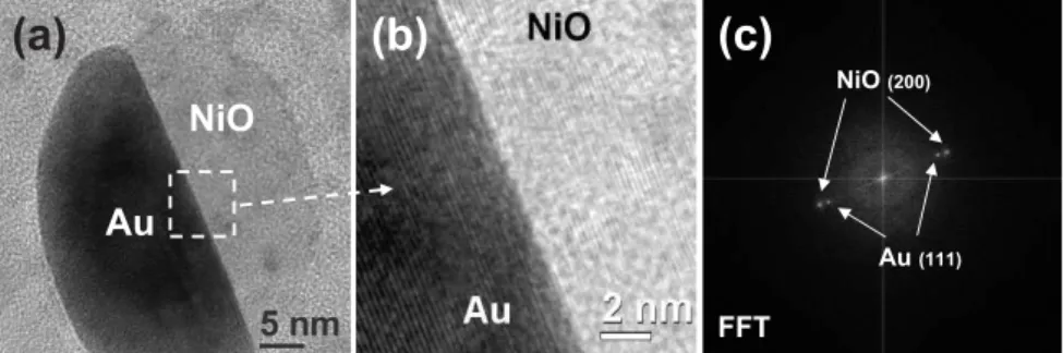
In Figure 1a, we present a high-resolution TEM (HRTEM) image of a Au/NiO cookie-like nanocluster. Cross-section TEM measurements showed the presence of such clusters throughout the film thickness. Figure 1b shows a detail of the interface between Au and NiO at a higher magnification, from which the epitaxial growth at the interface can be clearly seen. Indeed, the Fourier transform (FT) of the HRTEM image (Fig. 1c) highlights the presence of two sets of parallel planes: the region with darker contrast in Figure 1b shows the lattice fringes of face-centered cubic (fcc) Au (111) planes (with in-terplanar distance d(111) = 0.236 nm), whereas a second smaller periodicity, arising from the region with brighter con-trast in Figure 1b, can be indexed as originating from fcc NiO (200) planes (d(200) = 0.207 nm). A closer inspection of the HRTEM image shows, in the NiO part of the cluster, the pres-ence of small amorphous zones superimposed on the crystal-line regions. This result suggests a possible islandlike growth of the oxide, directed by the underlying Au template. It is in-teresting to highlight that we obtained a similar twofold co-herent topology in studying the dealloying processes under thermal annealing for bimetallic Au–Cu nanoclusters in silica obtained by ion implantation,[14]where upon short annealing
in an oxidizing atmosphere Au–Cu alloy nanoclusters were converted to an fcc Au-rich phase partially surrounded by a coherent fcc Cu2O shell.
To further characterize the twofold composition of the clus-ter, we coupled scanning TEM (STEM) imaging with energy-dispersive X-ray spectroscopy (EDS) nanoanalysis. Figure 2 shows the STEM signal, collected with a high-angle annular
TION
–
[*] Prof. A. Martucci, Dr. D. Buso, Prof. M. Guglielmi Dipartimento di Ingegneria Meccanica–Settore Materiali Università di Padova
Via Marzolo 9, 35131 Padova (Italy) E-mail: [email protected] Prof. G. Mattei, Prof. P. Mazzoldi Dipartimento di Fisica
Università di Padova
Via Marzolo 8, 35131 Padova (Italy) Dr. M. L. Post
Institute for Chemical Process and Environmental Technology National Research Council of Canada
1200 Montreal Road, Ottawa, ON K1A 0R6 (Canada)
[**] This work was supported by the Ministero Dell’Università e della Ricerca Scientifica (MURST) within a “Progetto di Ateneo n. CPDA042175” project of Padova University.
dark-field detector (HAADF), from a group of clusters. The brighter contrast in the image indicates the heavier element (Au in our case). By scanning a 1 nm (full width at half maxi-mum; FWHM) electron probe on a single cluster (dashed line, Fig. 2a), we obtained by EDS the concentration profile re-ported in Figure 2b, which clearly indicates that the cluster consists of two parts: a Au region and a Ni-rich part. A corre-lation between Ni and O concentration profiles along the scan line was also observed (not shown in Fig. 2b), which is consis-tent with the presence of the NiO phase evidenced by the HRTEM and FT measurements (see Fig. 1c).
Data obtained in the HRTEM–STEM analyses have been used to model the optical absorption spectrum of the sample in the visible range. The experimental absorption curve is shown in Figure 3 and exhibits two main bands; the most in-tense band is centered at 613 nm and the other is a shoulder at about 530 nm.
To model both absorption bands, we redefined the unusual geometry of the twofold clusters in a way that is depicted in the inset of Figure 3, i.e., as a sum of spherical Au clusters (type 1 cluster) and a spherical core/shell structure (type 2 cluster) in which the Au core has the same size as the previous Au type and is surrounded by a shell of NiO. This two-compo-nent model is motivated and supported by the fact that the surface free electrons of Au experience direct dielectric cou-pling with the silica matrix from one side (type 1 cluster) and, on the opposite side, with the silica mediated by a thick shell
experimental spectrum by adding the contribution of type 1 clusters, which have a surface plasmon resonance (SPR) band at 530 nm in silica, with that of type 2 clusters, which exhibit a red-shift of the Au SPR band induced by the higher dielectric constant (e) of NiO (eNiO= 5.4) compared with that of silica
(eSiO2= 2.13), and account for the band at 613 nm. The agreement between the simulated and the experimental spec-trum is quite satisfactory, as shown in Figure 3. It is worth noting that the numeric fitting procedure resulted in a 1:1 ratio between the population of type 1 and 2 clusters, again consistent with the assumption of the model. The spherical approximation used in the present model takes into account, in an average sense, the observed presence of prolate and oblate cookie-like structures. Moreover, the same strategy has successfully been applied in defining the optical absorption of similar partial core/shell Au-Cu2O nanoclusters.[14,15] Comparable simulations made
by assuming ellipsoidal cluster shapes did not give the same level of agreement. Hence, the principal result of the optical simulation is that the most intense absorption band is con-trolled by dielectric coupling at the Au/NiO interface, which red-shifts the position of the Au SPR band. This is important for explaining the results of the influence of gas absorption on the optical response of the material, as shown below.
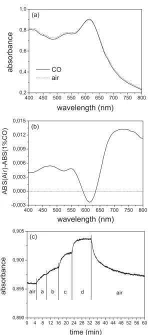
The gas sensing properties of the nanocomposite films were evaluated by measuring the variation of optical transmittance of the film when exposed to CO in air. The nanocomposite Au/NiO films exhibited clear and reversible absorbance changes in the vis-NIR wavelength region when exposed to CO, as shown in Figure 4. Upon exposure to 1 % CO, and
COMMUNICA
562 www.advmat.de © 2007 WILEY-VCH Verlag GmbH & Co. KGaA, Weinheim Adv. Mater.2007, 19, 561–564
5 nm
Au
NiO
Au(111) NiO(200) FFTFigure 1. a,b) High-resolution TEM (HRTEM) images of the twofold Au/NiO cluster topology. c) Fourier transform (FT) of the HRTEM image in (b), showing the presence of two sets of parallel planes in Au and NiO.
Au NiO 50 nm HAADF Detector 0 20 40 60 80 100 0 20 40 60 80 NiO Con c entra ti o n (at% ) scan depth (nm) Au Ni Au
(b)
(a)
Figure 2. a) HAADF dark field STEM image of Au/NiO clusters. The white dashed line indicates the scan direction of the compositional EDS profile analysis shown in (b).
400 500 600 700 800 0.0 0.2 0.4 0.6 0.8 1.0 Au-NiO film Mie fit absorbance wavelength (nm) Rcore(Au) = 5 nm tshell(NiO) = 10 nm NiO Au Au Au NiO = +
Figure 3.Experimental optical absorption spectrum of the sample (solid line) and corresponding effective medium fit (open circles) assuming a combination of monoelemental and core/shell nanoclusters. Absorbance is log10(incident light/transmitted light).
with the exception of wavelengths near the main plasmon ab-sorption band around 613 nm, there is a decrease in absor-bance over the whole wavelength range (Figure 4a). This fea-ture can be better appreciated when considering the data showing the absorbance in air minus absorbance in 1 % CO, defined as DA, reported in Figure 4b. The changes in absor-bance clearly display a dependence in magnitude and sign of DA with respect to wavelength. Thus, in the region of most in-tense absorption, (585 < k < 635 nm) there is a reversal of sign of the absorbance change (DA) in comparison with other wavelengths.
Similar behavior has been reported by Ando et al. for Co3O4 films containing Au nanoparticles exposed to H2.
However, that work reported only a positive DA for both
Co3O4–Au and NiO–Au nanocomposite films when exposed
to CO.[16,17]The present data is thus the first that provides evi-dence of negative DA in the plasmon wavelength region, which accompanies the exposure of nanoclusters with Au/NiO interfaces to CO. It is likely that the nanomorphology of the Au/NiO interface is intimately related to the existence of sup-pressed (or reversed) absorbance changes in the plasmon ab-sorbance range.
In NiO films that have no noble-metal component, the de-crease in absorbance is close to constant in the 350–850 nm wavelength range and is ascribed to a decrease in the positive hole density of NiO during catalytic oxidation of CO.[12]For the present case with NiO/Au, the decrease in absorbance at wavelengths outside the plasmon band can be ascribed to the same mechanism. The mechanism for the absorbance increase in the plasmon band is, however, not determined yet[16]but is
clearly associated with the mediated catalytic oxidation of the reducing gas (CO). One possible explanation could be related to electron injection from NiO into Au in the cookie-like Au/ NiO nanoparticles, thereby increasing the number of elec-trons available at the Au side of the Au/NiO interface that are involved in the catalytic oxidation of CO. This postulate is further supported considering that the variation in absorbance at 613 nm decreases as the CO concentration decreases (Fig. 4c). Further studies of the effect of bifurcation at a nano-interface on the key properties that influence the plasmon band (e.g., band position and width, permittivity, electrical conductivity, oxide species crystallite size) are required to ascertain the relative importance of the structural features presented here.
Experimental
The nanocomposites were prepared by mixing a matrix silica tion containing the precursors for silica and gold and a doping solu-tion containing the precursor for NiO. The precursor solusolu-tion for the silica matrix was made by mixing tetraethoxy silane (TEOS), methyl triethoxy silane (MTES), H2O, and HCl in EtOH according to molar ratios TEOS:MTES:H2O:HCl:EtOH = 1:1:4:0.02:4. HAuCl4· 3H2O was used as the metallic gold precursor and added directly in the ma-trix solution according to a Ni:Au = 5:1 molar ratio. The NiO precur-sor solution was made mixing NiCl2·6H2O in EtOH in the presence of N-[3-(trimethoxysilyl)propyl]-ethylenediammine (DAEPTMS) keeping the molar ratio of Ni:DAEPTMS = 1. The double amminic groups of DAEPTMS coordinate the Ni2+cations in the solution while the silanic group ensures the homogeneous dispersion of cations dis-tributed inside the final SiO2network. A nominal SiO2:NiO molar ra-tio of 3:2 has been used. The two precursor sols were then mixed to-gether to obtain the final batch [9b].
Films were deposited on quartz glass substrates via the dip-coating technique using a withdrawing speed of 100 cm min–1at 23 °C and controlled relative humidity (RH = 25 %). Thermal annealing of the films was performed in air at 700 °C for 60 min.
Structural and compositional characterization was performed at CNR-IMM (Bologna, Italy) on cross-sectional samples of the compos-ite films. Measurements were taken with a field-emission FEI TECNAI F20 SuperTwin FEG-(S)TEM microscope operating at
TION
400 450 500 550 600 650 700 750 800 0,2 0,4 0,6 0,8 1,0absorbance
wavelength (nm)
CO air (a) 400 450 500 550 600 650 700 750 800 -0,003 0,000 0,003 0,006 0,009 0,012 0,015 A B S(A ir) -A BS(1%CO) (b) 0 4 8 12 16 20 24 28 32 36 40 44 48 52 56 60 0,890 0,895 0,900 0,905 d c b air absorbance time (min) air a (c)wavelength (nm)
Figure 4.a) Absorption spectra of Au/NiO nanocomposite film in dry air (dotted line) and after exposure to 1 vol % CO (solid line). b) Absorbance in dry air minus absorbance in 1 % CO (DA) of the Au/NiO nanocomposite film. c) Absorbance measured at 613 nm and different CO concentrations (a = 10, b = 100, c = 1000, d = 10 000 ppm) of the Au/NiO nanocomposite film. Absorbance is log10(incident light/transmitted light).
charge-coupled device (CCD) array. Scanning TEM (STEM) analysis coupled with EDS allowed compositional analysis on single clusters by means of line scans with an electron probe resolution of 1 nm FWHM.
Optical sensor functionality was studied by performing optical ab-sorbance/transmittance measurements over the wavelength range 350 < k < 800 nm with sample films mounted on a heater in a custom built gas flow cell. Transmission data were recorded with a Varian Cary1E spectrophotometer with films heated at T = 330 °C (operating temperature) and for exposure to different CO concentrations in dry air. The substrate size for these measurements was approximately 1 cm × 2 cm and the incident spectrophotometer beam was normal to the film surface and covering a 6 mm × 1.5 mm section area.
Received: April 28, 2006 Revised: July 19, 2006 Published online: January 25, 2007
–
[1] Y. Yin, A. P. Alivisatos, Nature 2005, 437, 664.
[2] T. Trindade, P. O’Brien, N. L. Pickett, Chem. Mater. 2001, 13, 3843. [3] C. Noguez, Opt. Mater. 2005, 27, 1204.
[4] F. Caruso, Adv. Mater. 2001, 13, 11.
[5] Y. Xia, P. Yang, Y. Sun, Y. Wu, B. Mayers, B. Gates, Y. Yin, F. Kim, H. Yan, Adv. Mater. 2003, 15, 353.
Coord. Chem. Rev. 2005, 249, 1870.
[8] I. Hotovy, J. Huran, P. Siciliano, S. Capone, L. Spiess, V. Rehacek, Sens. Actuators, B 2001, 78, 126.
[9] a) T. Kobayashi, M. Haruta, M. Ando, Sens. Actuators, B 1993, 545, 13. b) D. Buso, M. Guglielmi, A. Martucci, G. Mattei, P. Mazzoldi, C. Sada, M. L. Post, Nanotechnology 2006, 17, 2429.
[10] X. Wang, G. Sakai, K. Shimanoe, N. Miura, N. Yamazoe, Sens. Actua-tors, B 1997, 45, 141.
[11] M. Matsumiya, W. Shin, N. Izu, N. Murayama, Sens. Actuators, B
2003, 93, 309.
[12] M. Ando, T. Kobayashi, M. Haruta, Catal. Today 1997, 36, 135. [13] A. Martucci, M. Pasquale, M. Guglielmi, M. Post, J. C. Pivin, J. Am.
Ceram. Soc. 2003, 86, 1638.
[14] G. Mattei, G. De Marchi, C. Maurizio, P. Mazzoldi, C. Sada, V. Bello, G. Battaglin, Phys. Rev. Lett. 2003, 90, 085 502.
[15] G. Battaglin, E. Cattaruzza, C. Julián Fernández, G. De Marchi, F. Gonella, G. Mattei, C. Maurizio, P. Mazzoldi, A. Miotello, C. Sada, F. D’Acapito, Nucl. Instrum. Methods Phys. Res. Sect. B 2001, 175, 410.
[16] M. Ando, T. Kobayashi, S. Iijimac, M. Haruta, J Mater. Chem. 1997, 7, 1779.
[17] M. Ando, T. Kobayashi, M. Haruta, J. Chem. Soc. Faraday Trans.
1994, 90, 1011.