Publisher’s version / Version de l'éditeur:
JOURNAL OF APPLIED PHYSICS, 107, 103701, pp. 1-11, 2010-05-18
READ THESE TERMS AND CONDITIONS CAREFULLY BEFORE USING THIS WEBSITE. https://nrc-publications.canada.ca/eng/copyright
Vous avez des questions? Nous pouvons vous aider. Pour communiquer directement avec un auteur, consultez la première page de la revue dans laquelle son article a été publié afin de trouver ses coordonnées. Si vous n’arrivez pas à les repérer, communiquez avec nous à PublicationsArchive-ArchivesPublications@nrc-cnrc.gc.ca.
Questions? Contact the NRC Publications Archive team at
PublicationsArchive-ArchivesPublications@nrc-cnrc.gc.ca. If you wish to email the authors directly, please see the first page of the publication for their contact information.
NRC Publications Archive
Archives des publications du CNRC
This publication could be one of several versions: author’s original, accepted manuscript or the publisher’s version. / La version de cette publication peut être l’une des suivantes : la version prépublication de l’auteur, la version acceptée du manuscrit ou la version de l’éditeur.
For the publisher’s version, please access the DOI link below./ Pour consulter la version de l’éditeur, utilisez le lien DOI ci-dessous.
https://doi.org/10.1063/1.3415527
Access and use of this website and the material on it are subject to the Terms and Conditions set forth at
Growth kinetics and electronic properties of unintentionally doped
semi-insulating GaN on SiC and high-resistivity GaN on sapphire grown
by ammonia molecular-beam epitaxy
Tang, H.; Fang, Z.Q.; Rolfe, S.; Bardwell, J.A.; Raymond, S.
https://publications-cnrc.canada.ca/fra/droits
L’accès à ce site Web et l’utilisation de son contenu sont assujettis aux conditions présentées dans le site LISEZ CES CONDITIONS ATTENTIVEMENT AVANT D’UTILISER CE SITE WEB.
NRC Publications Record / Notice d'Archives des publications de CNRC:
https://nrc-publications.canada.ca/eng/view/object/?id=d604c531-9506-4a68-8087-18334b29b9e7 https://publications-cnrc.canada.ca/fra/voir/objet/?id=d604c531-9506-4a68-8087-18334b29b9e7Growth kinetics and electronic properties of unintentionally doped
semi-insulating GaN on SiC and high-resistivity GaN on sapphire
grown by ammonia molecular-beam epitaxy
H. Tang,1,a兲 Z. Q. Fang,2S. Rolfe,1J. A. Bardwell,1and S. Raymond1
1
Institute for Microstructural Sciences, National Research Council Canada, Ottawa, Ontario K1A 0R6, Canada
2
Semiconductor Research Center, Wright State University, Dayton, Ohio 45435, USA
共Received 27 November 2009; accepted 26 March 2010; published online 18 May 2010兲
Growth of unintentionally doped 共UID兲 semi-insulating GaN on SiC and highly resistive GaN on sapphire using the ammonia molecular-beam epitaxy technique is reported. The semi-insulating UID GaN on SiC shows room temperature 共RT兲 resistivity of 1011 ⍀ cm and well defined activation
energy of 1.0 eV. The balance of compensation of unintentional donors and acceptors is such that the Fermi level is lowered to midgap, and controlled by a 1.0 eV deep level defect, which is thought to be related to the nitrogen antisite NGa, similar to the “EL2” center 共arsenic antisite兲 in
unintentionally doped semi-insulating GaAs. The highly resistive GaN on sapphire shows RT resistivity in range of 106– 109 ⍀ cm and activation energy varying from 0.25 to 0.9 eV. In this case, the compensation of shallow donors is incomplete, and the Fermi level is controlled by levels shallower than the 1.0 eV deep centers. The growth mechanisms for the resistive UID GaN materials were investigated by experimental studies of the surface kinetics during growth. The required growth regime involves a moderate growth temperature range of 740– 780 ° C, and a high ammonia flux 共beam equivalent pressure of 1 ⫻ 10−4 Torr兲, which ensures supersaturated coverage of surface adsorption sites with NHx radicals. Such highly nitrogen rich growth conditions lead to
two-dimensional layer by layer growth and reduced oxygen incorporation. © 2010 American
Institute of Physics. 关doi:10.1063/1.3415527兴
I. INTRODUCTION
Semi-insulating or high-resistivity GaN materials are re-quired for important device applications such as high power, high frequency transistors, and diodes. Because of strong tendency of acquiring n-type residual impurities and native defects such as oxygen and nitrogen vacancies, it has always been a challenge to achieve insulating GaN materials by various growth methods. Various approaches have been em-ployed to compensate these residual donors by intentional doping with Mg, C, Fe, etc. Among them, carbon doping and iron doping methods are demonstrated as effective doping schemes to obtain semi-insulating GaN with all major growth techniques such as hydride vapor phase epitaxy 共HVPE兲,1,2 metal-organic chemical vapor deposition 共MOCVD兲 共Refs. 3–5兲 and molecular-beam epitaxy 共MBE兲.6–8Intentionally doped GaN played important role in the development of nitride based electronics. The heavily doped semi-insulating GaN materials are mainly used as thick buffer layers in GaN HEMT devices. However, concern still exists as to possible deterioration of electrical or optical performance associated with carrier trapping, short effective carrier lifetime,9growth quality degradation, or memory ef-fect of the compensation impurities. In that regard, uninten-tionally doped 共UID兲 semi-insulating or high-resistivity GaN have advantages especially when used for the active regions
of devices such as HEMT, PIN diodes, and high voltage Schottky diodes, and when efficiency associated with long carrier lifetime is required.
There have been reports of UID high-resistivity GaN grown by various growth techniques. The high-resistivity UID GaN materials grown by MOCVD generally contain high carbon concentrations and high dislocation densities.4 High-resistivity UID GaN was also reported for the plasma-assisted MBE technique but few details on growth mecha-nisms and no electrical data on “semi-insulating” status GaN have been reported.10–12There have been also several reports of high resistivity UID GaN on grown on SiC or sapphire substrates with the ammonia-MBE technique.13,14Again, no detailed study of electrical properties and mechanisms analy-sis has been reported. In fact, high-reanaly-sistivity UID GaN has been routinely grown on silicon wafers by ammonia-MBE, as part of the GaN HEMT-on-silicon recipe developed by a group in France.15–17 However, the limited resistivity 共usu-ally in the order of 104 ⍀ cm兲 of the resistive silicon
sub-strate itself prevented accurate study of the resisitivity and compensation mechanisms of the GaN epilayers.
In the present article, we report achievement of UID semi-insulating GaN on SiC and high-resistivity GaN on sapphire using the ammonia-MBE growth technique. The ideal growth conditions were analyzed with help of investi-gation into the basic growth kinetics of the ammonia-MBE process. The electrical properties and defect levels were studied by temperature dependent dark current 共TDDC兲 mea-surements and thermally stimulated current 共TSC兲
spectros-a兲Author to whom correspondence should be addressed. Electronic mail:
haipeng.tang@nrc.ca.
copy. SIMS and photoluminescence data were also collected to facilitate the interpretation of the electrical properties.
II. EXPERIMENTAL METHODS
The growth system used for this study is an SVTA ni-tride MBE 共model N35S兲 equipped with an ammonia injec-tor with ammonia flow capacity up to 200 SCCM 共SCCM denotes cubic centimeter per minute at STP兲. The system also features carbon-doping capability using a saddle-field low energy ion source and methane source gas.18 The sub-strate temperatures were calibrated by pyrometer measure-ments. In order to understand a wide range of growth param-eters and growth regimes reported for ammonia-MBE growth by various authors, we performed an experimental study of ammonia cracking and nitride surface incorporation kinetics using the hydrogen surface desorption spectroscopy methodology. The desorbed hydrogen from ammonia crack-ing on a stationary or a growcrack-ing GaN surface 共i.e., with or without Ga flux supplied兲 was measured by a quadruple mass spectrometer. The difference of the hydrogen partial pressure measured when the ammonia flux is directed on the surface and when the ammonia flux is shuttered away is treated as a measure of the amount of the hydrogen released from the ammonia surface cracking and lattice incorporation reac-tions. In order to cover a wide range of growth conditions reported in the literature, and especially to understand the conditions to grow high-resistivity GaN materials, measure-ments were performed for a wide range of temperatures from 300 to 900 ° C, and ammonia flux from 5 to 200 SCCM. The Ga flux, when applied, was fixed at a beam equivalent pres-sure 共BEP兲 of 1.1⫻ 10−6 Torr corresponding to a growth rate of about 1 m / hr.
2 in. sapphire and 4H SiC substrates 共both repolished by NOVASIC Inc.兲 were used for the growth experiments. For both types of substrate, the cleaning procedure before load-ing for growth includes flushload-ing by boiled chloroform vapor, hydrogen fluoride 共HF兲 dip and 10 min deionized 共DI兲 water rinse and drying by nitrogen. Ideal growth conditions for achieving semi-insulating or high-resistivity GaN were found to include high ammonia flux, appropriate temperature window, and two-dimensional 共2D兲 growth mode. In order to understand the different growth mechanisms for both highly resistive and conducting GaN layers, GaN samples have been grown under varied growth temperature and ammonia flux to represent the most typical growth regimes used in practical growth. For both sapphire and SiC substrates, a 1000 Å thick AlN grown at 900 ° C was used as a buffer layer. In situ reflection high energy electron diffraction 共RHEED兲 was used to monitor the growth mode during growth. Both conducting and insulating GaN layers grown have been analyzed by secondary ion mass spectroscopy 共SIMS兲, atomic force microscopy 共AFM兲, and low tempera-ture PL 共photoluminescence兲. PL spectra were measured at 10 K with a He–Cd laser excitation at wavelength of 325 nm. The electrical properties and defect mechanisms in the semi-insulating or high-resisitivity GaN samples were investigated using TDDC measurements, photoconductivity measure-ments, and TSC spectroscopy.
III. AMMONIA CRACKING KINETICS AND GROWTH REGIMES
For ammonia MBE growth, the active nitrogen species are provided by the thermal cracking of the ammonia mol-ecules incident on the growing surface. In order to under-stand the growth mechanisms with the ammonia MBE tech-nique, it is crucial to understand the cracking behavior of ammonia molecules. In a study of GaN selective area growth, Gupta et al. measured ammonia cracking efficiency on various substrate materials without incident Ga flux, using the hydrogen desorption method. Mesrine et al.20 studied ammonia cracking efficiencies by monitoring the optical re-flectivity of predeposited Ga thin 共a few monolayers兲 layers during exposure to an ammonia flux. The latter study has determined ammonia cracking efficiency as a function of temperature from 250 up to 830 ° C under an incident Ga flux. It has shown that the cracking efficiency becomes sig-nificant above 450 ° C and reaches about 3.8% or slightly more for temperatures above 700 ° C. Crawford et al.21have studied both gallium and hydrogen desorption using the de-sorption mass spectroscopy technique. They have found that under Ga rich growth conditions, the excess gallium adatoms block adsorption sites for ammonia, and thus reduce the growth rates. Based on these studies and other growth data, Karpov et al.22 developed a detailed surface kinetics model for interpretation of available experimental and growth data. This model assumes an adsorption layer consisting of gal-lium adatoms and adsorbed NHx radicals. The model takes
into account specific effects of the blocking of NH3 adsorp-tion sites by the coverage of these surface species.
In the present work, we measured the ammonia cracking efficiency using the hydrogen desorption method for a wide range of temperature and ammonia flux parameters covering most typical growth regimes reported in the literature. Par-ticularly, we obtained experimental data for the difference of ammonia cracking efficiencies on a GaN surface with or without an incident Ga beam for a wide temperature range. Such data help to provide insight into the different growth mechanisms for the different growth regimes reported in the literature.
Figure1 shows the ammonia cracking efficiency on sta-tionary GaN surface 共without incident Ga flux兲, as repre-sented by the desorbed hydrogen pressure, as a function of the incident ammonia flux at various substrate temperatures. This graph shows the saturation of cracking with increasing ammonia flux. This confirms the assumption by Karpov et
al.22that saturated adsorption sites blocks further adsorption of ammonia molecules. A new ammonia molecule can be adsorbed only if an adsorption site is replenished after a pair of NHx radicals recombine and are desorbed as N2 and H2.
Since the desorption rate of the NHx radicals is thermally
activated, the ammonia cracking efficiency on nongrowing, stationary GaN surface shows strong temperature depen-dence.
In Fig.2, for a fixed ammonia flux of 70 SCCM 共BEP = 3.5⫻ 10−5 Torr兲, the desorbed hydrogen pressure is
mea-sured as a function of temperature. In Fig. 2共a兲, one set of data is for cracking measurement on nongrowing GaN
sur-face, and the other set is for growing GaN surface with in-cident Ga flux corresponding to BEP of 1.1⫻ 10−6 Torr 共equivalent to 1 m / hr兲. Noticeably, in the lower tempera-ture range 共⬍800 ° C兲, the reaction between Ga adatoms and NHx radicals, which results in GaN lattice incorporation,
greatly increased the hydrogen desorption rate. However, the two curves approach each other toward the high temperature end 共⬎800 ° C兲. To illustrate this trend more clearly, the dif-ference is taken by subtracting the two curves and replotted in Fig. 2共b兲. The data shown in Fig. 2共b兲can be understood as the contribution to hydrogen desorption due to Ga atoms reacting with an adsorbed NHxradical. The reaction leads to
hydrogen release and GaN lattice growth. The reaction also speeds up the replenishing rate of the adsorptions sites, since the sites blocked by adsorbed NHx radicals become new available adsorption sites following the Ga+ NHx⇒GaN + H2 reaction. That explains the increase in ammonia crack-ing with an incident Ga beam over most of the temperature range in Fig.2共a兲.
Figure2共b兲reveals three temperature zones of different characteristics. We find that these zones can be related to the different growth regimes used by various authors in the prac-tical growth work. The low temperature Zone I 共350 to 550 ° C兲 the differential hydrogen desorption rate shows a quick decline below 550 ° C. This indicates that the reaction efficiency between Ga adatoms and adsorbed NHx radicals
becomes insufficient to cause 100% lattice incorporation of the Ga adatoms. As a result, metal gallium accumulates on the surface, blocking nitrogen adsorption sites, and reducing the growth rate. The reduction of growth rate under Ga rich conditions has been well documented and interpreted in Refs.21–23.
In zone II 共550 to 800 ° C兲, the differential hydrogen desorption rate is basically constant with temperature, within the margin of error for the measurement method used. This means that in this temperature range, the Ga+ NHx⇒GaN
+ H2 reaction rate is constant, limited by the fixed Ga
inci-dent flux. In the entire zone II, and especially in the lower
temperature portion, Ga sticking coefficient is close to unity, i.e., minimal re-evaporation rate. The growing GaN surface is still saturated with adsorbed NHx radicals over the entire
temperature range of zone II. This is the typical nitrogen rich growth regime where growth rate is constant and depends only on Ga flux.
In zone III 共800 to 900 ° C兲, we observe a rapid drop of the differential hydrogen desorption rate when the tempera-ture increases above 800 ° C. This is because of the signifi-cantly elevated ammonia self-cracking rate associated with the NHx+ NHx⇒N2+ H2 reaction, which is now faster than
and dominates over the Ga+ NHx⇒GaN+ H2lattice
incorpo-ration reaction in this high temperature range. This can be seen from Fig.2共a兲. The desorbed hydrogen pressure on sta-tionary GaN surface without incident Ga increased to 2 ⫻ 10−5 Torr at 880 ° C, which far exceeded the maximum
hydrogen release pressure of about 3 ⫻ 10−6 Torr due to
GaN incorporation as indicated by the plateau level in both Figs.2共a兲 and2共b兲. We can see the two curves in Fig.2共a兲
approaches each other in this high temperature range. This means that GaN incorporation is no longer a rate-limiting event for ammonia cracking. Instead, the adsorbed NHx
radi-cals are desorbed rapidly via NHx+ NHx⇒N2+ H2reaction,
resulting in very short dwell time on the adsorption sites. In
T (C) 400 500 600 700 800 900 Desorbed Hy drogen (Torr) 1e-7 1e-6 1e-5 1e-4
ammonia cracking under Ga flux ammonia cracking without Ga flux
T (C) 300 400 500 600 700 800 900 Difference in desorbed hy drogen (Torr) 1e-7 1e-6 1e-5
difference in ammonia cracking with and without Ga flux
(a)
(b)
I
II
III
FIG. 2. 共a兲 Cracking efficiency of ammonia 共70 SCCM, BEP= 3.5
⫻ 10−5 Torr兲 on GaN surface as represented by desorbed hydrogen partial
pressure as a function of temperature, measured with or without an incident
Ga flux 共BEP= 1.1⫻ 10−6 Torr兲, and 共b兲 Difference between the ammonia
cracking efficiencies with and without the Ga flux.
Ammonia flow (sccm) 0 20 40 60 80 100 Hyd rogen desorption (T orr) 10-8 10-7 10-6 10-5 350 C 562 C 601 C 662 C 712 C 756 C 796 C 815 C Ammonia flow (sccm) 0 20 40 60 80 100 Hyd rogen desorption (T orr) 10-8 10-7 10-6 10-5 350 C 562 C 601 C 662 C 712 C 756 C 796 C 815 C
FIG. 1. Ammonia cracking efficiency on stationary GaN surface 共without incident Ga flux兲, as represented by the desorbed hydrogen partial pressure, as a function of the incident ammonia flux at various substrate temperatures.
other words, the self desorption of the adsorbed nitrogen species 共independent of the reaction with Ga兲 is fast enough so that the adsorption sites on the GaN surface are no longer saturated or blocked by them. This is a very important fea-ture for growth performed in zone III, as opposed to growth performed in zone II. In this article, we will attempt to asso-ciate practical growth results, especially the growth mecha-nisms of semi-insulating GaN materials with the surface ki-netics features discussed here.
Practical growth of GaN materials and devices by am-monia MBE has been performed by various groups using a range of temperature and ammonia flux parameters. These parameters generally fall into several growth regimes opti-mized for different purposes on the material. Zone I 共350 to 550 ° C兲 conditions in Fig. 2共b兲have rarely been applied to any practical growth, except maybe for attempt to grow InN or InGaN materials. Most practical growth regimes are nitro-gen rich growth, where the growth rate is constant, and lim-ited only by the supplied Ga flux.
For a given gallium flux 共BEP= 1.3⫻ 10−6 Torr兲, on
varying the nitrogen flux, the nitrogen rich to gallium rich transition point can be observed from the change in the mea-sured growth rate. As shown in Fig.3, at moderate tempera-ture of 770 ° C, the growth rate is constant when ammonia flow rate is greater than 8 SCCM but drops abruptly when the ammonia flow is decreased below 8 SCCM. The transi-tion at 8 SCCM ammonia 共BEP= 4.5⫻ 10−6 Torr兲
corre-sponds to V / III= 1 condition where V represents cracked and incorporated ammonia flux. The transition from nitrogen-rich to Ga-rich growth results in gallium surface accumulation and reduction in growth rate.21–23 For higher substrate tem-peratures, as shown in Fig. 3, this transition becomes less abrupt because the gallium sticking probability can no longer be assumed to be unity.
The characteristics of nitrogen rich growth as a function of growth temperature are illustrated in Fig.4. With ammo-nia flux set at 100 SCCM 共BEP= 5 ⫻ 10−5 Torr兲, the growth rate is constant up to about 880 ° C, beyond which the growth rate starts to drop due to GaN thermal decomposition and accelerated desorption of adsorbed species.
In a previous paper, we analyzed some of the most fre-quently seen growth regimes in the literature.24 Historically, in the authors’ laboratory, a growth regime using a high tem-perature 共840– 880 ° C兲 just below the GaN thermal decom-position threshold point and a moderate ammonia flux 共100 SCCM, BEP= 5 ⫻ 10−5 Torr兲 has been established and
ap-plied for GaN high-electron-mobility transistors 共HEMT兲 de-vices on sapphire and SiC substrates.25,26 In this growth re-gime, the growth is via a three-dimensional 共3D兲 mode, yielding facetted surface morphology but also large grain size, low defect density, and high electron mobility, mainly due to the higher growth temperature used.25Unintentionally doped GaN grown in this regime is always n-type conduct-ing. As a solution, we developed a carbon doping method using a low energy methane ion source, which successfully compensates all residual donors and yields semi-insulating GaN materials required for the HEMT devices.18 On the other hand, another growth regime employing a moderate growth temperature 共740– 780 ° C兲 and high ammonia flux 共ⱖ200 SCCM, BEPⱖ 1 ⫻ 10−4 Torr兲 has been established
for the development of GaN HEMT on Si 共111兲 wafers.15–17 Growth in this regime is via 2D mode, yielding excellent surface and interface smoothness. In addition, the GaN layers grown in this regime are highly resistive without any inten-tional doping, satisfying the requirement of resistive buffer layers for HEMT devices.15–17Similar layer-by-layer growth conditions have also been used for growth of GaN/InGaN or GaN/AlGaN quantum well structures 共on sapphire sub-strates兲 where interface smoothness is important.27–29
In Fig. 4, we marked on the growth rate curve with shadow windows for the 3D and 2D growth regimes dis-cussed above. To help interpretation of the growth mecha-nisms, the hydrogen desorption data in Fig.2共b兲are redrawn and overlapped with the growth rate characteristics in Fig.4. Clearly, the 2D growth regime falls into the higher tempera-ture part of the zone II region of Fig.2共b兲, whereas the 3D growth regime falls into the zone III region. It should be mentioned that growth in the lower temperature part 共550 to 710 ° C兲 of zone II of Fig.2共b兲 yields 3D columnar growth and inferior quality, and thus rarely applied in practical growth.13 Such observation may give insight into the
corre-NH3flow rate (sccm) 0 20 40 60 80 100 120 G rowth rate (µ m/ h r) 0.5 1.0 1.5 770 C 840 C 890 C Ga rich Nitrogen rich
FIG. 3. For a given Gallium flux 共BEP= 1.3⫻ 10−6 Torr兲 and several
sub-strate temperatures, the nitrogen rich to gallium rich transition point is de-termined from the change in the measured growth rate on varying the nitro-gen flux.
FIG. 4. The characteristics of nitrogen rich growth as a function of growth
temperature for ammonia flow rate of 100 SCCM 共BEP= 5 ⫻ 10−5 Torr兲 and
Gallium flux of BEP= 1.3⫻ 10−6 Torr. The hydrogen desorption data in Fig.
lation between the different surface kinetics 共adsorption, cracking, desorption, and incorporation兲 and the mechanisms behind the different growth modes and the resultant electrical properties.
IV. HIGH-RESISTIVITY GAN VERSUS CONDUCTING GAN
In this section, we present a detailed comparison of the typical growth and material characterization results for semi-insulating 共or high-resistivity兲 and conducting UID GaN by ammonia MBE. A carbon-doped semi-insulating GaN sample was also included in the study for comparison and interpretation purposes.
Semi-insulating 共or high-resistivity兲 UID GaN layers have been successfully obtained on SiC 共Cree semi-insulating 2
⬙
wafer兲 and sapphire 共2⬙
wafer兲 substrates using the 2D growth regimes described in Fig. 4. The growth pa-rameters for the GaN growth are: 760 ° C for growth tem-perature, 200 SCCM 共BEP= 1 ⫻ 10−4 Torr兲 for ammoniaflux, 0.8 m / hr for growth rate, and 1.3 m for growth thickness. The conditions for the AlN buffer layer were given in the previous section about the experimental methods. One semi-insulating UID GaN sample grown on SiC is denoted as sample A. Another high-resistivity UID GaN sample grown on sapphire is denoted as sample B. For comparison, one n-type, conducting UID GaN sample, denoted as sample C, has been grown on a sapphire substrate using the 3D growth regime described in Fig. 4, with growth parameters being: 870 ° C for growth temperature, 100 SCCM 共BEP = 5 ⫻ 10−5 Torr兲 for ammonia flux, 1 m / hr for growth
rate, and 1.3 m for thickness. A carbon-doped semi-insulating GaN sample, denoted hereafter as sample D, was also grown in the 3D regime on a SiC substrate, using simi-lar growth parameters as sample C. Details about carbon doping were published previously.18
Figure5 shows in situ RHEED patterns and AFM sur-face images for samples A, B, and C. The RHEED patterns clearly show that the growth was 2D growth for the two highly resistive UID GaN samples A and B, and was 3D for the conducting sample C. From the AFM micrographs, the surfaces of samples A and B, with root-mean-square 共rms兲
roughness of about 4 nm, are considerably smoother than that of sample C with rms roughness of 19 nm. Samples A and B basically show relatively flat 共0001兲 surface with a quite high density of small pits which may be associated with the terminations of threading dislocations. In contrast, the surface of sample C shows dominant 共10–1 m兲 pyramidal microfacets and vanishing 共0001兲 top facet.
The surface kinetics discussed in the previous section may be part of the underlying reasons for the very different surface morphologies revealed in Fig. 5. The growth condi-tions for samples A and B falls into the zone II in Fig.2共b兲, which is characterized by a nitrogen rich surface coverage. The high surface coverage of nitrogen species was further ensured by employing the maximum ammonia flow rate of 200 SCCM 共BEP= 1 ⫻ 10−4 Torr兲 designed for the MBE
system. According to the kinetic model of Karpov et al.,22 under such conditions, the adsorption sites are saturated and blocked by a layer of adsorbed NHx radicals, preventing
ni-trogen atoms from evaporating 共dissociation兲 from the step edges of the crystal. The adsorbed nitrogen species desorb slowly in the temperature range of zone II 共550– 800 ° C兲 of Fig.2共b兲, as can be seen by the low ammonia cracking rate on stationary GaN surface in Fig. 2共a兲. However, upon cap-turing Ga adatoms migrating to step edges, GaN incorpora-tion via the Ga+ NHx⇒GaN+ H2reaction occurs at a faster
rate, which speeds up the nitrogen cracking processes and the refreshing rate of the adsorption sites following the GaN in-corporation, making them available for adsorption of new ammonia molecules. That is why in the entire zone II, after the gallium flux is supplied to the GaN surface, the ammonia cracking rate is increased by an almost flat amount corre-sponding to the fixed Ga flux used. The growth temperature used 共760 ° C兲 is at the higher end of zone II, in order to provide sufficient surface mobility for Ga adatoms to diffuse to step edges, island edges where they can be attached to the lattice, and thus enabling 2D growth of the film. On the other hand, the growth temperature is still low enough, so that the step or nucleation island edges are still stable and saturated by adsorbed nitrogen species. Therefore, the kinetics in this regime is favorable for 2D nucleation and growth, resulting in smooth surface morphology. We find that UID GaN layers grown under such conditions on SiC or sapphire are electri-cally highly resistive, as will be characterized in detail in the next section.
On the other hand, the growth conditions with growth temperature at 870 ° C for the conducting GaN sample C fall into the zone III of Fig. 2共b兲, where ammonia cracking rate on stationary GaN surface is significantly enhanced. The much enhanced cracking and desorption rate of the adsorbed nitrogen radicals indicates reduced blocking of adsorption and incorporation sites on the surface, and reduced blocking of nitrogen atoms escaping from crystal from step edges. This increases the likelihood of 3D nucleation and growth. At this high temperature range, the step edges are no longer thermally stable, and nitrogen atoms can easily decompose and dissociate from the edges. A consequence of the unstable step edge is that the Ga atoms can move up the edge, and react with nitrogen radicals to form a new layer on top. As a result, multilayers with closely bunched multiple steps are
(a) (b) (c)
FIG. 5. In situ RHEED patterns and AFM surface images 共1 ⫻ 1 m2scan
and 90 nm/div in vertical direction兲 for 共a兲 sample A: semi-insulating UID GaN/SiC, 共b兲 sample B: high-resistivity UID GaN/sapphire, and 共c兲 sample C: conducting UID GaN/sapphire.
formed. In other words, the 共0001兲 surface is no longer a stable facet under such conditions. The 3D growth involving creation of densely bunched steps eventually leads to domi-nating microfacets of the 兵10–1 m其 pyramidal nature. As the AFM image for sample C shows, the 共0001兲 top facet com-pletely vanished on the surface. The pyramidal facets of course lead to significantly rougher surface than samples A and B grown under the 2D conditions. The UID GaN layers grown under the 3D growth conditions are found to be al-ways conducting with electron concentrations usually in the range of 1016– 1017 cm−3 range.
In order to know impurity incorporation levels in UID GaN layers grown under the 2D and 3D conditions, we per-formed SIMS measurements for samples A, B, and C. An-other carbon-doped GaN sample D was also included for comparison purpose. The results are presented in Table I. First, we notice that the oxygen levels in the 2D samples A and B are significantly lower than that in the 3D sample C. The carbon concentrations, on the other hand, are similar in all three samples. This trend is similar to what we reported in a previous study about growth regimes on SiC substrates.24 This phenomenon suggests that oxygen incorporation is in-hibited by the 2D surface kinetics, whereas carbon incorpo-ration is insensitive to the surface kinetics. Under the 2D growth regime, the saturated coverage of adsorbed NHx radi-cals in the adsorption layer likely blocks the adsorption and incorporation of oxygen atoms but cannot block the carbon species. Compared with the carbon doped GaN sample D, the oxygen and carbon concentrations in the UID GaN samples 共A, B, and C兲 are lower by one order and more than two orders of magnitude, respectively. This confirms that the highly resistive property of the UID samples A and B is not simply due to impurities but rather caused by intrinsic de-fects as will be discussed in the next section. Of course, the reduced oxygen levels in samples A and B may have contrib-uted to better carrier compensation in them.
We performed low temperature photoluminescence PL measurements on the four samples 共A, B, C, and D兲 as de-scribed above. The low resolution and wide wavelength range PL spectra are shown in Fig. 6共a兲, and the high reso-lution PL spectra for the band-edge region in Fig. 6共b兲. The conducting GaN sample C shows the highest exciton emis-sion intensity, whereas the highly resistive GaN samples A and B show reduced exciton peak intensity. The carbon-doped GaN sample 共D兲, on the other hand, show nearly dis-appeared emission in the exciton region. The spectrum for the carbon-doped GaN sample is dominated by a broad yel-low luminescence band. All the UID GaN samples, on the other hand, show much weaker yellow luminescence.
Several features can be observed by comparing the spec-tra. First, the PL properties of the highly resistive UID GaN samples are similar to those of the conducting UID GaN sample. Note that the slight shift of the exciton peak to higher wavelength for sample A is due to the tensile strain cause by the thermal mismatch with the SiC substrate used for this sample. All the UID samples show prominent exciton emissions and the well recognized shallow D-A pair emis-sions starting at about 3.28 eV. The yellow luminescence band is very weak in all the UID GaN samples. Common residual donors in ammonia MBE grown GaN include oxy-gen, silicon, and nitrogen vacancies.30Acceptors may result from carbon 共CN兲, nitrogen interstitial 共NI兲, and Ga
vacan-cies etc.31 The intensity of the exciton emission seems to relate inversely with the resistivity of the UID GaN. The most insulating sample A shows the lowest intensity. This suggests there are more abundant nonradiative recombina-tion centers in the highly resistive materials, which may cor-relate with the deep centers that are also responsible for pin-ning the Fermi level in the semi-insulating materials. The PL intensity and resistivity do not seem to correlate in any ob-vious manner with the line defects in these samples. The
TABLE I. SIMS measurement data for samples A: semi-insulating UID GaN/SiC, B: high-resistivity UID GaN/sapphire, C: conducting UID GaN/ sapphire, and D: semi-insulating, carbon-doped GaN/SiC.
Sample A B C D Oxygen 共cm−3兲 3 ⫻ 1017 4 ⫻ 1017 9 ⫻ 1017 3 ⫻ 1018 Carbon 共cm−3兲 8 ⫻ 1016 6 ⫻ 1016 8 ⫻ 1016 3 ⫻ 1019 Hydrogen 共cm−3兲 2 ⫻ 1018 3 ⫻ 1018 3 ⫻ 1018 2 ⫻ 1019
(a)
(b)
FIG. 6. Low temperature PL spectra: 共a兲 low resolution and wide wave-length range, 共b兲 high resolution in the band-edge region, for the four samples A: semi-insulating UID GaN/SiC, B: high-resistivity UID GaN/ sapphire, C: conducting UID GaN/sapphire, and D: semi-insulating, carbon-doped GaN/SiC.
x-ray rocking curve full-width-at-half-maximum of the 共0002兲 reflection are 633, 666, 446, and 360 arcsec for sample A, B, C, and D, respectively.
Second, we notice that the PL of the high-resistivity UID GaN is very different from that of the carbon-doped, high-resistivity GaN material. The carbon-doped material shows near complete quenching of the exciton emissions and the D-A pair emissions. Only the yellow luminescence band is observable even at such low temperature 共10 K兲. The lumi-nescence properties of the carbon-doped GaN have been re-ported and discussed in a previous paper.9 Because of the high carbon 共in the order of 1019 cm−3兲 and associated
oxy-gen 共in the order of 1018 cm−3兲 concentrations, radiative
re-combination of excitons is suppressed by prevailing nonra-diative recombination centers that were introduced by the carbon-doping process. The nonradiative centers may in-volve carbon and oxygen impurities and their complexes formed with native defects. The yellow luminescence is the only remaining radiative recombination channel in the carbon-doped GaN material. There have been extensive re-search and debate on the origin of the notorious yellow lu-minescence 共YL兲 in GaN. General consensus points to two possible transition mechanisms for the YL. The first ascribes the YL to a transition between shallow donors and a deep acceptor level about 0.9 eV above the valence band. The deep acceptors are formed by Ga vacancies 共VGa兲, or more
likely VGa– ONcomplexes.9,31–33The second model ascribes
the YL to a transition from the split deep levels 共1.6 and 2.3 eV above valence band兲 formed by carbon interstitials 共CI兲 in
carbon-doped GaN materials to shallow acceptors or the va-lence band.34–36 Substitutional CN atoms form shallow ac-ceptor states at about 0.2 eV above the valence band.37,38 Gallium vacancies/complexes are likely the dominant origin of YL in n-type GaN because the formation energy of VGais
lower when the Fermi level is near the conduction band.31 Carbon impurities may be the dominant contributors to the YL in semi-insulating GaN where the Fermi level is lowered to midgap. Given the high carbon concentration of 1019 cm−3 in our sample D, it is very possible that most
carbon atoms incorporated as interstitials, creating a large density of deep level defects, some of which contribute to the YL. The fact that the yellow luminescence is much stronger in the carbon-doped sample than in the UID samples may suggest much higher density of the carbon interstitials 共CI兲 in
the former than the density of gallium vacancies in the latter. This is understandable given the carbon doping in the level of 1019 cm−3. Native defects like gallium vacancies are
un-likely to reach that level. Also the shallow donor to gallium vacancy 共deep acceptor兲 transition depends on spatial over-lap of the two centers. Relatively low densities of such cen-ters, and thus large spatial separation between them, and competition from other recombination channels, may explain the weak yellow luminescence in the UID GaN samples here. The carbon-related deep states can act both as radiative recombination centers and nonradiative recombination centers.39 It has been observed that the impurities/defects responsible for the YL also shorten the lifetime of nonequi-librium carriers.39 Such an interpretation is consistent with the PL spectrum of the carbon-doped GaN sample D. We see
that the band-edge exciton emission as well as the shallow D-A pair emission is completely quenched, presumably by the carbon impurity nonradiative centers introduced at large densities, given the high carbon doping concentration in this sample.
The highly resistive and semi-insulating UID GaN, on the other hand, still shows dominant exciton emissions and D-A pair emissions. The shallow acceptor involved in the D-A pair emission is most likely CN, since Mg doping had
not been performed in our system for several years prior to this work. Because of significantly lower carbon concentra-tions in the order of 1016 cm−3, CNmay account for a large
portion of all the carbon atoms incorporated in the UID ma-terials. This indicates that there are significantly fewer non-radiative centers in the high-resistivity UID material than in the carbon-doped material. The yellow luminescence in the UID material is also much weaker, consistent with the lower carbon incorporation level. In conclusion, compared with carbon-doped GaN, the high-resistivity UID GaN material is markedly cleaner in terms of impurities and defect centers, and is superior in optical properties and carrier lifetimes, and thus more suitable for use in active regions of certain device applications.
V. HIGH RESISTIVITY MEASUREMENT RESULTS
The layer grown on the SiC substrate, i.e., sample A, shows very good uniformity in electrical properties across the wafer. Figure 7共a兲 shows the dc dark current versus 1000/T characteristics measured with 100 V bias for two pieces 共7 ⫻ 7 mm2 in size兲, cut from the sample A. One piece used In contacts, while the other used annealed Ti/ Al/Au metal contacts. The temperature dependent dc charac-teristics show well-defined activation energy of 1.02 eV. The room temperature resistivity is about 1011 ⍀ cm. Therefore,
the UID GaN material grown on SiC is truly semi-insulating, with electrical conductivity governed by a deep level at 1.0 eV. On the other hand, the resistive UID GaN samples grown on sapphire substrates, i.e., the sample B and other similar samples, show quite significant nonuniformity, i.e., variation in resistivity across the wafer, and from wafer to wafer. This could be related to insufficient surface quality of the sapphire substrates, in spite of the substrate repolishing performed by Novasic Inc. Figure7共b兲shows several dc dark current ver-sus 1000/T curves measured with 1 V bias on several pieces cut from sample B 共piece B100608e兲 and other similarly grown samples 共pieces B100408d and B140408兲. The room temperature resistivity varies from 106to 109 ⍀ cm. And the
measured resistivity activation energy in the high tempera-ture range varied from 0.25, 0.52, to 0.90 eV. Therefore, such UID GaN layers grown on sapphire substrates are highly resistive but do not attain “semi-insulating” status. The resistivity is governed by gap states of varying depth 共⬍0.9 eV兲 depending on incomplete compensation of elec-trically active impurities and dominant point-defect related deep centers, as observed by TSC characterization 共see be-low兲.
Figures 8共a兲 and 8共b兲 show the photoconductivity re-sponse at 82 K for two pieces from the sample A, and several
pieces from the sample B 共piece B100608e兲 and wafers simi-lar to sample B 共pieces B100408d and B140408兲, respec-tively. The semi-insulating UID GaN pieces on SiC 共sample A兲 show saturated photocurrent of 0.3– 1.4 A under 100 V bias and 400 nm light excitation. The high-resistivity UID GaN pieces, grown on sapphire 共sample B and similar wa-fers兲 show saturated photocurrent of 1.1–20 nA under 1 V bias and 400 nm light excitation. It is important to note that the photo response 共or photocurrent per 1 V兲 in both types of samples is many orders of magnitude higher than that in carbon-doped semi-insulating GaN materials. In a previous study,9 the carbon-doped GaN layers showed saturated pho-tocurrent of less than 0.2 pA under 100 V bias and 360 nm light excitation. This indicates that the UID semi-insulating/ resistive GaN materials have significantly longer effective carrier lifetime than the carbon-doped GaN materials. This is consistent with the photoluminescence results in the previous section, which revealed the near complete quenching of ex-citonic emissions in the carbon-doped GaN. The density of deep traps and recombination centers must be significantly increased due to the heavy carbon doping to levels of 1019 cm−3. Such deep centers could include carbon
intersti-tials 共CI兲, CGa– CI complexes, or carbon-oxygen-point
de-fects complexes.34–36 In the UID semi-insulating/resistive GaN materials, the carbon concentrations are much lower, in the order of 1016 cm−3. In this case, the carrier lifetime is much longer, and is limited mainly by intrinsic defects such as point defects. Long carrier lifetime is important for the efficiency of PIN diodes, Schottky diodes, and the base re-gion of transistors, for example. Short carrier lifetime, on the other hand, is required for high speed operation of the de-vices. Therefore, in theory, it is possible to tune the carrier lifetime value in a wide range between the values for the resistive UID GaN and the heavily carbon-doped GaN. This offers an advantage from device design point of view.
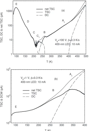
Typical net TSC spectra for pieces from the sample A 共with EA= 1.0 eV兲 and sample B 共from piece B140408 with
EA= 0.25 eV兲 are presented in Fig. 9, with TSC and dc shown together for comparison 共note that net TSC= TSC-dc兲. The broad E-trap peak at ⬃100 K, is very prominent in the sample A, and exists also in the sample B. From the TSC peak temperature Tm for a given trap, an approximate
acti-vation energy can be determined from an equation ET
= kTmln共Tm4/兲, where k is Boltzmann’s constant andthe
heating rate 共i.e., 0.3 K/s兲.40Trap E has activation energy of about 0.17 eV and has been identified with nitrogen vacancy in n-GaN layers by electron-irradiation study.41However,
de-0.1 1 10 100 1000 10000 2 3 4 5 6 7 8 9 10 metal contacts In contacts (a) EA=1.02 eV V b=100 V,β=0.3 K/s (measured upon cooling)
1000/T (1/K) DC (pA) 0.1 10 1000 100000 2 3 4 5 6 7 8 9 10 11 12 B140408 B100408d B100608e (b) E A3=0.90 eV E A2=0.52 e V EA1=0.25 eV Vb=1 V,β=0.3 K/s (measured upon cooling)
1000/T (1/K)
DC
(pA)
FIG. 7. 共a兲 TDDC vs 1000/T characteristics measured with 100 V bias for two pieces from sample A 共semi-insulating UID GaN/SiC兲, 共b兲 TDDC vs 1000/T characteristics measured with 1 V bias for pieces from sample B 共high-resistivity UID GaN/sapphire兲 and other similar UID GaN/sapphire sample. 10-2 100 102 104 106 0 60 120 180 240 300 360 420 480 In contacts metal contacts (a) PPC PC Light off Light on V b=100 V, T=82 K 400-nm LED: 10 mA Time (sec) PC (p A ) 0.1 10 1000 100000 0 60 120 180 240 300 360 B140408 (EA=0.25 eV) B100408d (EA=0.53 eV) B100608e (EA=0.90 eV) (b) PPC PC Light off Light on Vb=1 V, T=82 K 400-nm LED: 10 mA Time (sec) PC (pA)
FIG. 8. The photoconductivity response at 82 K measured with 400 nm light for 共a兲 two pieces from sample A 共semi-insulating UID GaN/SiC兲, and 共b兲 pieces from sample B 共high-resistivity UID GaN/sapphire兲 and similar UID GaN/sapphire samples.
tailed data fittings have revealed that the broad E-band actu-ally is the convolution of several traps E1 共0.07 eV兲, E2 共0.12 eV兲, E3 共0.21 eV兲, E4 共0.22 eV兲, and E5 共0.26 eV兲, among which E1 and E2 are electron traps, and E3–E5 are hole traps.42 The hole traps E3–E5 might been attributed to CN共Ref.43兲 or VGa.44The TSC spectra also revealed traps B
共0.52 eV兲 and Ax 共0.74 eV兲 in both samples. The trap B,
which is very weak in the samples A and B but is often the strongest trap in GaN grown by any method and not affected by electron-irradiation, could be due to CGa 共Ref. 44兲 or FeGa.45 The trap Ax is close to the trap A 共0.67 eV兲, which was observed in carbon doped GaN and has been associated with Ga vacancies in previous studies.9Other traps D 共0.24 eV兲, C 共0.30 eV兲, and C1共0.41 eV兲, which have been found in Fe-doped semi-insulating HVPE-grown GaN,45can be ob-served in the sample A, as shoulder features of the trap E.
In the following section, we attempt to interpret the na-ture of these dominant trap states, the correlation with the growth kinetics, and the effect on carrier compensation, transport, and recombination properties.
VI. INTERPRETATION OF COMPENSATION MECHANISMS
Attainment of semi-insulating status of “unintentionally doped” GaN requires a delicate balance among
concentra-tions of “unintentional” donor and acceptor impurities, de-fects, and defect-related deep level 共midgap兲. Unintentional donors may include oxygen 共ON兲, silicon 共SiGa兲, nitrogen vacancies 共VN兲, carbon 共CGa兲, etc. Unintentional acceptors
may include carbon 共CN兲, Ga vacancies 共VGa兲, other point
defect-impurity complexes etc. Based on what has been ob-served in the present study, we propose that there is a 1.0 eV deep donor level 共EC− 1.0 eV, denoted as “AY1” hereafter兲,
and we tentatively attribute it to nitrogen antisite NGa. This deep level in GaN is assimilated to the well known “EL2” center 共at EC− 0.75 eV兲 in unintentionally doped semi-insulating GaAs, where unintentional shallow acceptor is carbon and its concentration is higher than that of uninten-tional shallow donors. In fact, the 1.0 eV deep level has been observed in TDDC measurements of carbon-doped or Fe-doped semi-insulating GaN grown by MBE and HVPE.9,45 The deep level, as an extended-defect related electron trap A1, has been also widely observed by DLTS in n-type GaN and AlGaN/GaN heterostructures 共for example, see Ref.46兲. The results of the present work allude that this omnipresent native defect is very likely the nitrogen-antisite related de-fect, and it is the prominent native defect that controls the resistivity of unintentionally doped semi-insulating GaN, just like the EL2 defect 共related to arsenic antisite兲 in uninten-tionally doped semi-insulating GaAs. Previous studies have also associated the nitrogen antisite defect 共NGa兲 with deep
states at 0.8–1.1 eV below the bottom of the conduction band,47,48 which agrees well with the 1.0 eV activation en-ergy found in our TDDC measurements of the semi-insulating materials.
If the concentration of the unintentional shallow donors is ND, and the acceptors NA, then the hope is that NA⬎ ND
and existence of sufficient amount of the deep-donor levels, due to most prominently AY1 centers in the “unintentionally doped” GaN. Otherwise, the GaN would be p-type. When NAY1⬎ NA-ND⬎ 0 is satisfied, the Fermi energy is controlled by the partially occupied AY1 states, and semi-insulating be-havior results. We believe this scenario applies for the semi-insulating UID GaN grown on SiC, i.e., sample A. On the other hand, if the balance of compensation is such that NA-ND⬍ 0, the Fermi energy will be controlled by shallower defect species rather than AY1, and the material will attain highly resistive status rather than semi-insulating. We believe this is the case for the high-resistivity UID GaN grown on sapphire substrates, i.e., sample B and similarly grown samples.
Experimentally we find there is a prominent trap E band in the TSC spectrum for sample A. The E band consists of electron and hole traps, resulting from shallow donors, such as VN, and shallow acceptors, such as CNand VGa. On the
other hand, Ga vacancies or VGa– ON complexes can form
deep acceptors at about 0.8–1.0 eV above the valence. The total of the shallow and deep acceptors seems to be sufficient to compensate all the unintentional shallow donors such as oxygen and nitrogen vacancies. As a result, the Fermi level is lowered to the 1 eV deep level AY1, the partial occupancy of which dictates the activation energy of the resistivity. From the SIMS data, we do observe the lowest oxygen concentra-tion in the sample A. Although the measured oxygen
concen-1 10 100 1000 100 150 200 250 300 350 400 450 500 net TSC TSC DC (a) Ax B C1 C D E Vb=100 V,β=0.3 K/s 400-nm LED: 10 mA T (K) TSC, DC & net TSC (pA) 103 104 105 100 150 200 250 300 350 400 net TSC TSC DC (b) B Ax E Vb=1 V,β=0.3 K/s 400-nm LED: 10 mA T (K) TSC & DCW (pA)
FIG. 9. Typical net TSC spectra measured at= 0.3 K / s for 共a兲 sample A
共semi-insulating GaN/SiC兲 with 100 V bias and 400 nm light, and 共b兲 sample B 共high-resistivity UID GaN/sapphire兲 with 1 V bias and 400 nm light. TSC and dc are also presented in the figures for comparison.
tration is still higher than the carbon concentration, not all oxygen atoms incorporate as simple ON donors. Some of
them might contribute to VGa– ONacceptors, or incorporate in electrically inactive sites.
The TSC spectrum of sample B, on the other hand show only weak E band, which may indicate lower density of shal-low acceptor-type defects. The carbon impurities may have incorporated as interstitials or other complexes rather than the CNshallow acceptor. The oxygen concentration is higher
and carbon concentration is lower in sample B. As a result, the compensation of shallow donors is incomplete. The PL results in Fig.6also show higher donor-bound exciton inten-sity for sample B than for sample A.
Finally, the growth kinetics can shed some light on why formation of acceptor-type defects and nitrogen antisites is favored in the specific growth regime applied, while donor impurities and defects are suppressed. The 2D growth regime used for the semi-insulating 共or resistive兲 UID GaN materials is located in a particular temperature window, as marked in the growth characteristics graph in Fig. 4. The temperature window 共740– 780 ° C兲 is located in the higher end of the growth kinetics zone II. A key feature for zone II is that the GaN surface is saturated with adsorbed ammonia molecules. The preferred adsorption sites are step edges, defects etc. In this temperature zone, adsorbed ammonia molecules, mostly in the form of NHxradicals, crack thermally at a negligibly
slow rate, if no incident gallium flux is applied to the surface. However, when an incident gallium flux is supplied to the surface, the ammonia cracking rate is increased by a signifi-cant amount that is proportional to the gallium flux. Obvi-ously, the added ammonia cracking rate is due to the reaction between gallium and adsorbed ammonia species resulting in GaN lattice incorporation. It is anticipated such incorpora-tion of gallium and nitrogen atoms occurs preferentially at step edges following diffusion of gallium adatoms. As a re-sult, formation of GaN 2D nuclei and 2D growth/or step-flow growth can be maintained under such growth condi-tions. Another key factor is the high ammonia flux used. The V/III ratio, in terms of ammonia BEP 共1 ⫻ 10−4 Torr兲 to
gal-lium BEP 共1 ⫻ 10−6 Torr兲 ratio, reaches 100:1. The high
am-monia flux ensures saturated surface coverage of all available adsorption sites 共e.g., step edges兲. With such a moderate growth temperature and saturated ammonia surface cover-age, the key growth sites, namely the step edges, are ther-mally stable and blocked by adsorbed NHx radicals. The
blocking effect prevents nitrogen atoms from escaping the lattice from step edges,22 thus reducing the chance of form-ing nitrogen vacancies, a donor type defect. From SIMS analysis, the blocking effect also reduces incorporation at step edges of oxygen, another donor impurity. On the con-trary, the excess supply of nitrogen species at step edges encourages formation of Ga vacancies 共an acceptor type de-fect兲, and nitrogen antisites 共the 1.0 eV deep level defect兲. Therefore, we think the specific growth kinetics and condi-tions are responsible for the semi-insulating or highly resis-tive property of the UID GaN materials grown.
To explain why semi-insulating UID GaN is achieved only on SiC and the UID GaN layers grown on sapphire only achieved highly resistive status, we probably have to invoke
the different lattice mismatch with the two substrates and the interplay with line defects. The larger lattice mismatch be-tween GaN 共AlN兲 and sapphire than with SiC can result in higher density of threading dislocations and difference in the nature of such line defects, i.e., screw type, edge type, or mixed type. Interplay of the line defects with point defects and impurities could have prevented formation of sufficient unintentional shallow CN acceptors and deep gallium
va-cancy related “acceptors,” or have produced excessive unin-tentional “donors,” leading to not fully balanced compensa-tion. Depending on the types and density of the dislocations, the unintentional carbon and oxygen atoms may preferen-tially decorate the core region of dislocations, forming com-plexes rather than substitutional shallow levels. Neverthe-less, UID GaN with resistivity up to 109 ⍀ cm has been
demonstrated on sapphire substrates as well.
In the end, we would like to comment on the conditions for growth of n-type conducting UID GaN. In Fig. 4, if we venture into the high temperature zone III, i.e., T ⬎ 820 ° C, the growth kinetics is markedly changed. At such high tem-peratures, the ammonia self cracking rate on the GaN surface is markedly enhanced 关see Fig. 2共a兲兴, and is no longer de-pendent on the supply of the Ga flux 关see Fig. 2共b兲兴. This indicates that key surface features such as step edges are no longer thermally stable, and no longer effectively blocked by adsorbed ammonia species. In fact, kinetic roughening of an originally smooth GaN surface at such high temperature un-der an incident ammonia flux can be observed by in situ RHEED measurement. The surface roughening involves multiplication and bunching of steps, and eventually leads to facetted surface morphology as in Fig. 5共c兲. The kinetics is such that the growth mode is predominantly 3D facetted growth. The dense step edges on a facetted surface are favor-able for nitrogen atoms to escape from the crystal, creating nitrogen vacancies. Such growth mode also promotes oxygen incorporation as confirmed by the SIMS data in Table I. Therefore the 3D growth regime in the zone III of the kinet-ics chart in Fig.4produces n-type GaN conducting materials with prevailing amount of donor-type defects and impurities, as opposed to smaller amount of unintentional acceptors and deep level defects. Because of the high growth temperature, the n-type conducting UID GaN, with electron density typi-cally in the range of 1016– 1017 cm−3, exhibits excellent crystal quality as well as optical and electrical properties, despite of a relatively rough surface morphology. Bulk mo-bilities as high as 560 cm2/V s have been reported for
con-ducting GaN grown on sapphire substrates by ammonia MBE.49 It is impossible to obtain high-resistivity UID GaN using the 3D regime in Fig. 4. However, it is possible to grow semi-insulating carbon-doped GaN in the 3D regime. In fact, excellent GaN/AlGaN HEMTs have been routinely grown in our laboratory using the 3D growth regime com-bined with a carbon-doped semi-insulating GaN buffer.50,51 As discussed in the previous section, semi-insulating UID GaN or carbon-doped GaN each offers different advantages depending on specific device design for carrier lifetime, ef-ficiency, speed, and interface quality etc.
VII. CONCLUSIONS
Growth of semi-insulating UID GaN on SiC and highly resistive UID GaN on sapphire by ammonia MBE has been demonstrated. The growth regime and mechanisms have been investigated and elucidated with experimental studies of the surface kinetics during growth. The growth regime requires a moderate temperature range 共740– 780 ° C兲 and a high ammonia flux that ensures supersaturated adsorption coverage of the GaN surface. The key feature of the surface kinetics in this growth regime is that surface step edges are stable in this temperature range and that the step edges are blocked by adsorbed ammonia species which prevent nitro-gen atoms from escaping the lattice. Ga adatoms diffuse and incorporate at step edges, leading to 2D layer by layer growth mode. Such nitrogen rich growth kinetics was found to reduce donor type oxygen impurity incorporation, and is expected to discourage donor type nitrogen vacancies while encourage acceptor type Ga vacancies and a deep center: nitrogen antisite NGa. The semi-insulating UID GaN on SiC
exhibited a RT resistivity of 1011 ⍀ cm, and well defined
activation energy of 1.0 eV. The 1.0 eV deep center is thought to be related to an intrinsic defect: the nitrogen an-tisite NGa, similar to the “EL2” center 共related to AsGa兲 in insulating unintentionally doped GaAs. The semi-insulating behavior results from complete compensation of unintentional shallow donors by unintentional acceptors, and the Fermi level pinned to the partially occupied nitrogen an-tisite deep centers. The highly resistive UID GaN on sap-phire exhibited RT resistivity in a range from 106 to
109 ⍀ cm and activation energy varying from 0.25 to 0.9 eV.
The high resistivity behavior results from incomplete com-pensation of shallow donors, and the Fermi level controlled by levels shallower than the 1.0 eV deep nitrogen antisite center. The semi-insulating or highly resistive UID GaN ex-hibits orders of magnitude longer effective carrier lifetime than the insulating carbon-doped GaN. Therefore semi-insulating UID GaN can offer advantages in certain device applications such as PIN diodes, Schottky diodes, photocon-ductors, etc, when high efficiencies are required. On the other hand, as a lifetime shortening dopant, carbon-doping may be used to tune the carrier life time to desired values, when fast switching speed is required for certain applica-tions.
ACKNOWLEDGMENTS
The authors are indebted to S. Moisa and I. Sproule for SIMS measurements, G. Parent for AFM measurements, and L. Polenta for fitting the TSC measurement data.
1R. P. Vaudo, X. Xu, A. Salant, J. Malcarne, and G. R. Brandes,Phys.
Status Solidi A200, 18 共2003兲.
2J. A. Freitas, Jr., J. G. Tischlera, J.-H. Kimb, Y. Kumagaic, and A.
Kou-kituc,J. Cryst. Growth305, 403 共2007兲.
3S. Heikman, S. Keller, S. P. DenBaars, and U. K. Mishra,Appl. Phys. Lett.
81, 439 共2002兲.
4A. E. Wickenden, D. D. Koleske, R. L. Henry, M. E. Twigg, and M.
Fatemi,J. Cryst. Growth260, 54 共2004兲.
5M. Azize, M. Leroux, M. Laugt, P. Gibart, and Z. Bougrioua,Phys. Status
Solidi A203, 1744 共2006兲.
6A. Corrion, F. Wu, T. Mates, C. S. Gallinat, C. Poblenz, and J. S. Speck,
J. Cryst. Growth289, 587 共2006兲.
7F. Mei, Q. M. Fu, T. Peng, C. Liu, M. Z. Peng, and J. M. Zhou,J. Appl.
Phys.103, 094502 共2008兲.
8H. Tang, J. B. Webb, J. A. Bardwell, S. Raymond, J. Salzman, and C.
Uzan-Saguy,Appl. Phys. Lett.78, 757 共2001兲.
9Z.-Q. Fang, D. C. Look, B. Claflin, S. Haffouz, H. Tang, and J. Webb,
Phys. Status Solidi C2, 2757 共2005兲.
10M. J. Manfra, N. G. Weimann, J. W. P. Hsu, L. N. Pfeiffer, K. W. West,
and S. N. G. Chu,Appl. Phys. Lett.81, 1456 共2002兲.
11P. Kordos, P. Javorka, M. Morvic, J. Betko, J. M. Van Hove, A. M.
Wowchak, and P. P. Chow,Appl. Phys. Lett.76, 3762 共2000兲.
12M. Micovic, A. Kurdoghlian, P. Janke, P. Hashimoto, D. W. S. Wong, J. S.
Moon, L. McCray, and C. Nguyen,IEEE Trans. Electron Devices48, 591
共2001兲.
13A. L. Corrion, C. Poblenz, F. Wu, and J. S. Speck,J. Appl. Phys.103,
093529 共2008兲.
14W. Kim, O. Aktas, A. Salvador, A. Botchkarev, B. Sverdlov, S. N.
Mo-hammad, and H. Morkoc,Solid-State Electron.41, 169 共1997兲.
15F. Semond, P. Lorenzini, N. Grandjean, and J. Massies,Appl. Phys. Lett.
78, 335 共2001兲.
16N. Baron, Y. Cordier, S. Chenot, P. Vennéguès, O. Tottereau, M. Leroux,
F. Semond, and J. Massies,J. Appl. Phys.105, 033701 共2009兲.
17Y. Cordier, F. Semond, M. Hugues, F. Natalie, P. Lorenzini, H. Haas, S.
Chenot, M. Laugt, O. Tottereau, P. Vennegues, and J. Massies,J. Cryst.
Growth278, 393 共2005兲.
18J. B. Webb, H. Tang, S. Rolfe, and J. Bardwell,Appl. Phys. Lett.75, 953
共1999兲.
19V. K. Gupta, K. L. Averett, M. W. Koch, B. L. Mcintyre, and G. W. Wicks,
J. Electron. Mater.29, 322 共2000兲.
20M. Mesrine, N. Grandjean, and J. Massies, Appl. Phys. Lett. 72, 350
共1998兲.
21D. E. Crawford, R. Held, A. M. Johnston, A. M. Dabiran, and P. I. Cohen,
MRS Internet J. Nitride Semicond. Res. 1, 12 共1996兲.
22S. Y. Karpov, R. A. Talalaev, Y. N. Makarov, N. Grandjean, J. Massies,
and B. Damilano,Surf. Sci.450, 191 共2000兲.
23R. Held, D. E. Crawford, A. M. Johnston, A. M. Dabiran, and P. I. Cohen,
Surf. Rev. Lett.5, 913 共1998兲.
24H. Tang, S. Rolfe, F. Semond, J. A. Bardwell, and J. M. Baribeau,J. Cryst.
Growth311, 2091 共2009兲.
25J. B. Webb, H. Tang, J. A. Bardwell, S. Moisa, C. Peters, and T.
MacEl-wee,J. Cryst. Growth230, 584 共2001兲.
26H. Tang, J. B. Webb, J. A. Bardwell, S. Rolfe, and T. MacElwee,
Solid-State Electron.44, 2177 共2000兲.
27N. Grandjean and J. Massies,Appl. Phys. Lett.71, 1816 共1997兲.
28N. Grandjean and J. Massies,Appl. Phys. Lett.73, 1260 共1998兲.
29N. Grandjean, J. Massies, I. Grzegory, and S. Porowski,Semicond. Sci.
Technol.16, 358 共2001兲.
30D. C. Look, D. C. Reynolds, J. W. Hemsky, J. R. Sizelove, R. L. Jones,
and R. J. Molnar,Phys. Rev. Lett.79, 2273 共1997兲.
31J. Neugebauer and C. G. Van de Walle,Appl. Phys. Lett.69, 503 共1996兲.
32T. Ogino and M. Aoki,Jpn. J. Appl. Phys., Part 119, 2395 共1980兲.
33D. M. Hofmann, D. Kovalev, G. Steude, B. K. Meyer, A. Hoffmann, L.
Eckey, R. Heitz, T. Detchprom, H. Amano, and I. Akasaki,Phys. Rev. B
52, 16702 共1995兲.
34R. Armitage, W. Hong, Q. Yang, H. Feick, J. Gebauer, E. R. Weber, S.
Hautakangas, and K. Saarinen,Appl. Phys. Lett.82, 3457 共2003兲.
35W. You, X. D. Zhang, L. M. Zhang, Z. Yang, H. Bian, Q. Ge, W. X. Guo,
W. X. Wang, and Z. M. Liu,Physica B403, 2666 共2008兲.
36A. F. Wright,J. Appl. Phys.92, 2575 共2002兲.
37H. Wang and A.-B. Chen,Phys. Rev. B63, 125212 共2001兲.
38A. Armstrong, A. R. Arehart, B. Moran, S. P. DenBaars, U. K. Mishra, J.
S. Speck, and S. A. Ringel,Appl. Phys. Lett.84, 374 共2004兲.
39J. Mickevièius, R. Aleksiejunas, M. S. Shur, S. Sakalauskas, G.
Tamulai-tis, Q. Fareed, and R. Gaska,Appl. Phys. Lett.86, 041910 共2005兲.
40D. C. Look,Semicond. Semimetals19, 75 共1983兲.
41Z.-Q. Fang, J. W. Hemsky, D. C. Look, and M. P. Mack,Appl. Phys. Lett.
72, 448 共1998兲.
42L. Polenta and Z.-Q. Fang 共unpublished兲.
43S. Fischer, C. Wetzel, E. E. Haller, and B. K. Meyer,Appl. Phys. Lett.67,
1298 共1995兲.
44D. C. Look, Z.-Q. Fang, and B. Claflin,J. Cryst. Growth281, 143 共2005兲.
45Z. Q. Fang, B. Claflin, D. C. Look, S. Elhamri, H. E. Smith, W. C.
Mitchel, D. Hanser, E. A. Preble, and K. R. Evans,Phys. Status Solidi C
46Z.-Q. Fang, D. C. Look, D. H. Kim, and I. Adesida,Appl. Phys. Lett.87, 182115 共2005兲.
47T. L. Tansley and R. J. Egan,Physica B185, 190 共1993兲.
48T. Suski, P. Perlin, H. Teisseyre, M. Leszczynski, I. Grzegory, J. Jun, and
M. Bockowski,Appl. Phys. Lett.67, 2188 共1995兲.
49H. Tang and J. Webb,Appl. Phys. Lett.74, 2373 共1999兲.
50J. B. Webb, H. Tang, J. A. Bardwell, and P. Coleridge,Appl. Phys. Lett.
78, 3845 共2001兲.
51J. A. Bardwell, Y. Liu, H. Tang, J. B. Webb, S. J. Rolfe, and J. Lapointe,