HAL Id: pastel-00004551
https://pastel.archives-ouvertes.fr/pastel-00004551
Submitted on 10 Apr 2009
HAL is a multi-disciplinary open access
archive for the deposit and dissemination of
sci-entific research documents, whether they are
pub-lished or not. The documents may come from
teaching and research institutions in France or
abroad, or from public or private research centers.
L’archive ouverte pluridisciplinaire HAL, est
destinée au dépôt et à la diffusion de documents
scientifiques de niveau recherche, publiés ou non,
émanant des établissements d’enseignement et de
recherche français ou étrangers, des laboratoires
publics ou privés.
Architecture and design of a reconfigurable RF sampling
receiver for multistandard applications
Anis Latiri
To cite this version:
Anis Latiri. Architecture and design of a reconfigurable RF sampling receiver for multistandard
applications. domain_other. Télécom ParisTech, 2008. English. �pastel-00004551�
Architecture and design of a reconfigurable RF
sampling receiver for multistandard applications
Remerciements
Cette th`ese a ´et´e men´ee dans un premier temps au sein du groupe Syst`emes Int´egr´es Analogiques et Mixtes (SIAM) du d´epartement de Communications et ´
Electronique (COMELEC) `a T´el´ecom Paris, puis dans un second temps, chez l’industriel STMicroelectronics `a Crolles.
J’adresse mes remerciements au professeur Patrick Garda d’avoir accept´e de pr´esider mon Jury de th`ese. Je remercie ´egalement mes rapporteurs, les professeurs Andreas Kaiser et Pascal Fouillat pour l’int´erˆet qu’ils ont port´e `
a mon travail et pour leurs remarques et observations constructives. Je tiens aussi `a remercier Franck Montaudon et de nouveau Patrick Garda pour avoir examin´e ma th`ese.
J’exprime tout ma gratitude `a mon directeur de th`ese Patrick Loumeau et ma co-directrice Patricia Desgreys. Je les remercie du fond du coeur pour la confiance qu’ils ont su m’accorder, pour leur soutien continu tout au long de la th`ese et pour leur encadrement et conseils inestimables.
Je tiens `a remercier tous les ing´enieurs STMicroelectronics avec qui j’ai eu le plaisir de travailler durant la deuxi`eme partie de ma th`ese. Je remerice en particulier Daniel Sais, Loic Jo¨et et Franck Montaudon d’avoir accept´e de suivre mon travail de th`ese et de m’avoir fait profit´e de leur exp´erience technique durant la phase de concpetion de mon circuit int´egr´e. Toute ma gratitude va ´egalement `
a Fr´ed´eric Paillardet sans qui l’envoi en fonderie et la fabrication du circuit n’auraient pas eu lieu.
Une grande pens´ee `a tous mes amis et compagnons de route, th´esards, sta-giaires et post-doc avec qui j’ai partag´e d’inoubliables moments (je repense `a toutes ces pauses caf´e, matchs de foot du vendredi soir et pizzas `a la butte aux cailles) et sur qui je pouvais compter `a tout moment. Un grand merci donc `a Chadi, David, Denis, Eric, Ghassan, Joao, Manel, Marcia, Maya, Rayan, Richard, Sami, Sonia, ainsi qu’`a tous les autres. Je vous suis ´eternellement re-connaissant pour tous ces petits moments de bonheur. Je remercie ´egalement Karim Ben Kalaia pour sa gentillesse et pour son pr´ecieux coup de main lors de le phase d’´evaluation du circuit int´egr´e.
Je remercie aussi toute ma famille, en particulier mes parents, mes soeurs et mes beaux fr`eres. Leurs encouragements m’ont ´et´e d’un grand secours dans les moments difficiles de la th`ese. Enfin, un grand merci `a ma tr`es ch`ere ´epouse Semira pour tout le soutien qu’elle m’a apport´e et aussi pour sa patience et sa compr´ehension pendant les derniers mois de r´edaction.
Abstract
The fast development of wireless communication systems requires more flexible and cost effective radio architectures. A long term goal is the software defined radio, where communication standards are chosen by reconfiguration of hard-ware. Direct analog to digital conversion of the radio frequency (RF) signal is still unrealistic at present time, due to the high requirements imposed on the analog to digital converter. This motivates the need for a highly flexible RF analog front-end that can be fully integrated in low cost digital deep-submicron CMOS processes.
Different techniques for shifting the RF and analog circuit design complexity to digitally intensive domain were developed recently. These techniques are based on direct RF sampling and discrete-time analog signal processing and allow for a great flexibility and reduction of cost and power consumption in a reconfigurable design environment.
These concepts have been used in this thesis to develop a reconfigurable discrete-time radio receiver front-end. The circuit, which consists mainly of a transconductance low noise amplifier and two discrete-time analog signal pro-cessing stages, performs RF sampling, anti-alias filtering, frequency downcon-version, decimation and lowpass filtering.
To validate the flexibility and reconfigurability of the receiver, GSM and 802.11g communication standards have been addressed and adopted during sys-tem level study. The frequency plan and filtering scheme decided for each stan-dard were made different to fully analyze and validate the flexibility of the architecture. The circuit has been designed in 90nm CMOS technology and first measurement results demonstrated the functionality of the receiver.
Additionally, a fully passive 2ndorder discrete-time sinc type anti-alias filter has been described and included in the proposed receiver. Based on capacitive ratios for coefficient weighting, this filter is intended to considerably improve the alias filter rejection, which is one of the major problems reported in present discrete-time receivers. By changing the input sampling rate, the anti-alias filter can be tuned to different RF frequency bands and is hence suitable for true multi-standard operations.
Keywords: radio receivers, multi-standard, RF sampling, discrete time, analog signal processing, anti-aliasing filter
R´
esum´
e ´
etendu
Introduction
Le d´eveloppement rapide des communications sans fil et l’´emergence de nou-veaux standards ont sollicit´e la demande pour des r´ecepteurs radio multi-modes `
a faible coˆut. Pour des applications mobiles, un haut niveau d’int´egration, une grande flexibilit´e et une faible consommation sont les principales donn´ees `a res-pecter. Parmi les approches possibles pour le multi-standards, on retrouve la solution Software Defined Radio (SDR), qui consiste `a concevoir une chaˆıne de r´eception qui soit totalement reconfigurable par logiciel. Au passage d’un sch´ema de r´eception radio classique vers une architecture SDR, la majorit´e du traitement du signal effectu´e au niveau de la chaˆıne de r´eception est translat´ee en num´erique, ce qui impose des contraintes beaucoup plus s´ev`eres sur le conver-tisseur ADC (large bande, dynamique et taux d’´echantillonnage assez ´elev´es). La consommation excessive qui en r´esulte rend impossible l’impl´ementation du SDR dans les t´el´ephones mobiles.
Des techniques de traitement du signal analogique `a temps discret (bas´ees no-tamment sur les capacit´es commut´ees) peuvent ˆetre utilis´ees ici afin d’all´eger les contraintes impos´ees sur l’ADC. De plus, ce type de traitement pr´esente l’avan-tage d’ˆetre flexible et parfaitement reprogrammable. D’un autre cˆot´e, l’´evolution de la technologie submicronique permet d´esormais d’´echantillonner directement les signaux en bande RF. En combinant l’´echantillonnage RF au traitement du signal analogique temps discret, il est alors possible d’obtenir un r´ecepteur radio adapt´e au multi-standards et `a la software radio de fa¸con plus g´en´erale. Dans cette perspective, le signal RF re¸cu `a l’antenne serait amplifi´e, ´echantillonn´e puis trait´e de fa¸con analogique temps discret, avant d’ˆetre finalement num´eris´e par l’ADC. Ce type de r´ecepteur n´ecessite cependant un filtrage anti-alias avant ´echantillonnage qui doit ˆetre `a la fois performant et totalement reconfigurable.
Cette th`ese a deux objectifs bien sp´ecifiques. Le premier est de proposer une architecture reconfigurable pour un r´ecepteur multi-standards, bas´ee sur l’´echantillonnage passe-bande RF et sur le traitement de signal analogique `a temps discret. Bien que plusieurs r´ealisations de tels r´ecepteurs aient ´et´e d´ej`a rapport´ees, peu d’entre elles ont essay´e d’adresser diff´erentes normes de commu-nication afin de valider r´eellement l’aspect reconfigurabilit´e. Dans le travail de th`ese, les normes GSM900 et 802.11g (qui pr´esentent des caract´eristiques assez diff´erentes) ont ´et´e choisies comme r´ef´erences pour valider les m´ecanismes de reconfiguration et par cons´equent la reprogrammabilit´e du r´ecepteur.
Le deuxi`eme objectif de cette th`ese est d’´etudier et proposer de nouvelles structures de filtrage anti-alias d’ordres ´elev´es. Un filtre en peigne de second
10
ordre enti`erement passif a ´et´e analys´e et impl´ement´e dans le r´ecepteur propos´e. Ce filtre se pr´esente comme un filtre FIR `a temps discret dont les coefficients sont impl´ement´es `a l’aide de rapports capacitifs. Il permet d’am´eliorer la r´ejection d’alias sans surcoˆut de consommation et pr´esente l’avantage d’ˆetre totalement reconfigurable.
Architecture du r´
ecepteur
Le r´ecepteur propos´e repose sur une architecture assez semblable `a celles des radios `a temps discret d´ecrites dans la litt´erature. Cependant, il est sup-pos´e atteindre de meilleures performances en terme de r´ejection d’alias (grˆace au filtre en peigne de second ordre) et permet d’impl´ementer deux modes de communication diff´erents.
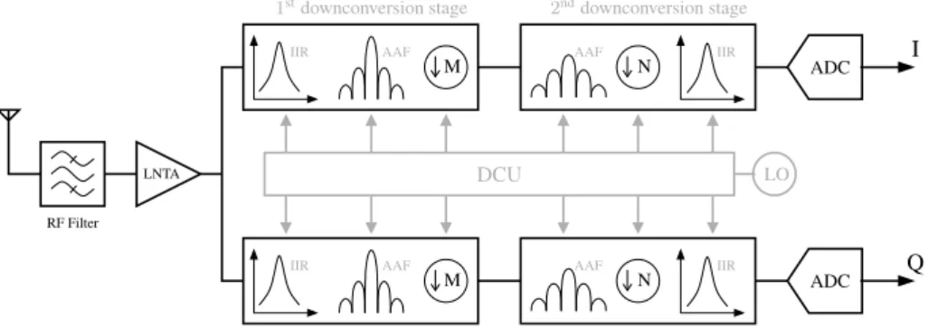
L’architecture du r´ecepteur est repr´esent´ee Figure 1. Elle comporte un filtre RF, un amplificateur faible bruit `a transconductance (LNTA), deux ´etages de traitement de signal analogique `a temps discret (DTASP) et deux convertisseurs analogique num´erique.
Le signal d’entr´ee RF est d’abord filtr´e, amplifi´e et converti en courant. Il est ensuite trait´e par un premier ´etage analogique `a temps discret, o`u il subit des op´erations de filtrage IIR/FIR et une translation en fr´equences vers une premi`ere fr´equence interm´ediaire. Un deuxi`eme ´etage de traitement permet de r´eduire la fr´equence d’´echantillonnage et de filtrer le signal `a fr´equence interm´ediaire avant la conversion analogique num´erique.
DCU LNTA ADC ADC M AAF IIR N AAF IIR M AAF IIR N AAF IIR RF Filter Q I LO 1stdownconversion stage 2nddownconversion stage
Figure 1. Architecture du r´ecepteur `a ´echantillonnage RF
Le courant en sortie du LNTA est int´egr´e pendant une p´eriode 4F1
c (Fc
´
etant la fr´equence du canal RF) `a travers une capacit´e histoire (formant le fitlre IIR) et une capacit´e unitaire (appartenant au filtre anti-repliement) de fa¸con continue et commut´ee entre les voies en quadrature I et Q. Il en r´esulte un flux d’´echantillons temps discret `a une fr´equence 2Fc par voie I/Q.
Le filtrage IIR, r´ealis´e par un simple pˆole, est n´ecessaire en sortie du LNTA afin d’´eviter toute saturation en pr´esence d’´eventuels signaux bloqueurs. Le second ´etage permet ensuite de r´eduire le taux d’´echantillonnage (d´ecimation) tout en ´evitant le repliement des signaux adjacents (filtre FIR) et d’apporter le filtrage canal n´ecessaire (IIR) afin de respecter la dynamique d’entr´ee de l’ADC.
11
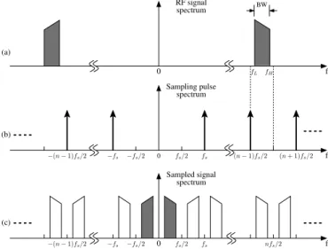
Plan de fr´
equences
Le plan de fr´equence utilis´e en mode GSM est donn´e Figure 2. Le signal utile est toujours centr´e `a la moiti´e de la fr´equence d’´echantillonnage (r´ecepteur en Fs/2) afin d’´eviter les d´egradations li´ees au bruit en 1/f et aux produits
d’intermodulation d’ordre 2.
5 FIR 2 9 IIR 2 ADC
(SINC2) FIR 1 IIR 1 Fs= 1.8 GHz signal @ Fc Fs= 360 MHz signal @ Fs/2 Fs= 40 MHz signal @ Fs/2 2ndDTASP 1stDTASP Fc 900 MHz
Figure 2. Plan de fr´equences en mode GSM
Le premier rapport de d´ecimation est impos´e par le filtrage anti-repliement, la r´ejection ´etant directement proportionnelle au rapport de la bande passante par la fr´equence d’´echantillonnage. Dans le cas du GSM, il a ´et´e d´ecid´e de r´eduire la fr´equence d’´echantillonnage `a 360 MHz en sortie du premier ´etage de traitement analogique, soit un rapport de d´ecimation M1´egal `a 5.
Le second ´etage doit adapter le taux d’´echantillonnage `a la fr´equence de fonctionnement de l’ADC, soit 40 MHz. Le deuxi`eme rapport de d´ecimation M2
a donc ´et´e fix´e `a 9, le signal utile se retrouvant ainsi en sortie `a une fr´equence de 20 MHz.
Le plan de fr´equence utilis´e en mode 802.11g est donn´e Figure 3. Le signal utile s’´etalant sur plus de 10 MHz de bande passante, le bruit en 1/f devient alors moins signifiant. L’architecture en Fs/2 ne pr´esente plus de r´eels int´erˆets
et il devient donc envisageable de translater le signal directement en bande de base.
4 (SINC2) FIR 1
IIR 1 FIR 2 2 IIR 2 ADC
Fs= 600 MHz signal @ DC Fs= 4.8 GHz signal @ Fc Fs= 1.2 GHz signal @ DC Fc 2.4 GHz 1stDTASP
Figure 3. Plan de fr´equences en mode 802.11g
Le signal RF est tout d’abord ´echantillonn´e `a la fr´equence 2Fc (de fa¸con
similaire au mode GSM). Les filtres IIR et anti-alias du premier ´etage restent centr´es autour du canal RF (sch´ema en Fs/2). Le signal est ensuite translat´e en
bande de base par l’utilisation d’un facteur de d´ecimation pair (M1= 4).
Le deuxi`eme ´etage de traitement analogique `a temps discret (non impl´ement´e dans le circuit actuel) r´ealise une seconde s´erie de filtrages IIR/FIR ainsi qu’une d´ecimation par 2 afin de conditionner le signal et permettre sa num´erisation par un convertisseur analogique num´erique d´edi´e.
12
Filtre anti-repliement
Le filtrage anti-repliement r´ealis´e en tout d´ebut de chaˆıne de conversion doit ˆ
etre centr´e sur la fr´equence canal Fc et pr´esenter des z´eros de transmission aux
fr´equences des alias situ´es `a Fc± kFs. En traitement de signal num´erique, il
est possible de r´ealiser facilement des filtres passe bande si la fr´equence centrale est la moiti´e de la fr´equence d’´echantillonnage (F s/2). Ceci explique la raison pour laquelle le signal RF est ´echantillonn´e `a la fr´equence 2Fc en tout d´ebut de
chaˆıne.
Les coefficients du filtre anti-repliement de second ordre propos´e ici ont ´et´e calcul´es `a partir de la fonction de transfert d’un filtre en peigne (moyenne glis-sante) de longueur ´egale au rapport de d´ecimation M = 2Fc/Fs. En ´elevant au
carr´e la fonction de transfert puis en effectuant une transformation passe bas vers passe haut (z−1→ −z−1), on obtient les coefficients d’un filtre de second
ordre centr´e en Fc et ayant des z´eros de transmission tous les kFs. La fonction
de transfert du filtre anti-repliement est donn´ee par :
H(z) = TL→H M −1 X k=0 z−k !2 = M −1 X k=0 (−1)kz−k !2
Les coefficients qui en d´ecoulent sont donn´es dans le Tableau 1 pour les deux modes de fonctionnement (GSM et 802.11g). Notons que la longueur du filtre est ´egale `a 2M (ce qui ´equivaut `a une dur´ee de traitement ´egale `a 2Ts) et qu’il
faut donc disposer de deux chaˆınes d’int´egration en parall`ele afin de conserver un taux d’´echantillonnage ´egal `a 1/Ts.
mode ↓ M ratio FIR coefficients
GSM 5 [+1 -2 +3 -4 +5 -4 +3 -2 +1 0]
WIFI 4 [+1 -2 +3 -4 +3 -2 +1 0]
Tableau 1. Coefficients du filtre FIR en modes GSM et 802.11g
Les coefficients du filtre sont impl´ement´es au niveau circuit en utilisant une technique de division de charges passive. Chaque coefficient se voit affecter un vecteur de M capacit´es unitaires. Le courant d’entr´ee est d’abord int´egr´e sur le vecteur entier durant une p´eriode Ti = Tc/4. Afin de r´ealiser le keme
coef-ficient, on vient ensuite pr´elever la charge stock´ee uniquement sur k capacit´es unitaires du vecteur, r´ealisant ainsi une fraction |αk| = k/M de la charge
ini-tialement int´egr´ee. Le signe et la partie complexe de chaque coefficient sont form´es ult´erieurement lors de la connexion des k capacit´es vers la sortie du filtre (connexion directe ou invers´ee vers une des deux voies en quadrature). La divi-sion de charges est pr´esent´ee Figure 4 pour le mode GSM, o`u l’impl´ementation des coefficients du filtre anti-repliement n´ecessite un vecteur de 5 capacit´es uni-taires par coefficient.
Une structure `a trois voies parall`eles `a entrelacement temporel a ´et´e utilis´ee afin de conserver un taux d’´echantillonnage ´egal `a 1/Tsen sortie du filtre
anti-alias (cf. Figure 5 pour le mode GSM). A un instant t donn´e, deux voies sont connect´ees en entr´ee et int`egrent le courant d’entr´ee, tandis que la troisi`eme voie est connect´ee en sortie pour la lecture de la charge puis est r´einitialis´ee. La compl´ementarit´e entre les coefficients des voies parall`eles permet d’utiliser le
13 from Gm φin φin φin φin φin Ci Ci Ci Ci Ci φo1 φo1 φo1 φo2 φo2 α = 2/5 α = 3/5
Figure 4. Impl´ementation des coefficients par division de charges
mˆeme vecteur de M capacit´es unitaires pour la r´ealisation de deux coefficients diff´erents, r´ealisant ainsi un gain consid´erable en surface et en nombre de signaux de commande. +3 -4 +5 -4 +3 -2 +1 0 Output + Reset +1 -2 +3 0 +1 -2 +3 -4 +5 -4 +3 -2 +1 0 +1 -2 Output + Reset +1 -2 +3 -4 +5 -4 +3 -2 O + R O + R path 3 path 2 path 1 Ti
Figure 5. Voies d’int´egrations parall`eles en mode GSM
Les performances du filtre anti-repliement propos´e sont limit´ees uniquement par les disparit´es capacitives (mismatch inh´erent `a la technologie utilis´ee). Pour des disparit´es de l’ordre de σ(∆C/C) = 0.1%, la profondeur des z´eros de trans-mission est limit´ee `a 75 dB, soit la moiti´e de la r´ejection calcul´ee th´eoriquement. Les performances du filtre propos´e restent n´eanmoins meilleures `a celles d’un simple filtre anti-alias d’ordre un. Notons ´egalement que la complexit´e li´ee `a la structure du filtre croit en fonction du nombre et des valeurs des coefficients `
a impl´ementer. Le nombre de signaux de commande n´ecessaires augmente la consommation du bloc num´erique responsable de la g´en´eration des phases d’hor-loge, ainsi que la pollution g´en´er´ee par la commutation signaux de commande dans les parties analogiques sensibles du circuit.
´
Etude syst`
eme du r´
ecepteur
L’´etude syst`eme du r´ecepteur propos´e s’est limit´ee `a la sp´ecification et la r´epartition des gains, bruits et filtrages le long de la chaˆıne de r´eception. L’am-plificateur faible bruit LNTA ´etant le seul bloc actif du r´ecepteur, le bruit rajout´e par les blocs en amont doit ˆetre le plus bas possible. Notamment, la perte de gain li´ee aux capacit´es parasites et au moyennage passif des charges devront ˆetre minimis´es. Le filtrage n´ecessaire est principalement dict´e par les dynamiques en sortie du LNTA et `a l’entr´ee du convertisseur analogique num´erique. Ce filtrage
14
se traduit au niveau circuit par les valeurs des capacit´es histoires des filtres IIR, une fois la valeur des capacit´es unitaires fix´ee.
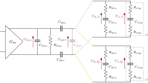
Une analyse nodale a ´et´e effectu´ee sur un circuit simplifi´e repr´esentant le premier ´etage de traitement analogique `a temps discret (Figure 6). Cette analyse a permis d’obtenir les tensions aux bornes des capacit´es rotatives et histoires (avec un gain de temps consid´erable par rapport `a des simulations ´electriques standards) et d’en d´eduire les valeurs r´eelles des gains et filtrages IIR pour des valeurs de capacit´es donn´ees.
Rsig Rhis Rsig Rhis x5 Rsig Rhis Rsig Rhis x5 Cdec Cdec Clna Gm Cpar Rlna Ulna Upar Uh,I Us,Q Uh,Q Us,I Chis Csig Csig Chis
Figure 6. Sch´ema ´electrique utilis´e lors de l’´etude syst`eme
La contribution en bruit thermique des deux ´etages de traitement analogique `
a temps discret a ´et´e minutieusement calcul´ee et a permis d’extraire les valeurs des capacit´es unitaires et rotatives des filtres FIR anti-repliement. Les gains et bruits des diff´erents ´etages de la chaˆıne de r´eception sont r´esum´es dans le Tableau 2 pour le mode GSM et permettent d’estimer la valeur de la sensibilit´e que pourra atteindre le r´ecepteur (−102dBm en GSM900, soit le minimum requis par la norme).
ANTENNA SWITCH SAW LNTA SINC2 FIR2/IIR2 ADC
Noise Figure dB 0.0 1.0 2.8 2.5
Noise Contribution V^2 1.27E-11 8.89E-11 1.99E-10
Power Gain dB 0.0 -1.0 -2.8 37.4
Voltage Gain dB 24.4 -2.28 0.0 0.0
Output Signal Level dBmdBVrms -102.0-115.0 -103.0-116.0 -105.8-118.8 -81.4 -83.7 -83.7 -83.7 Output Noise Level dBmdBVrms -121.0-134.0 -121.0-134.0 -121.0-134.0 -94.1 -96.1 -94.8 -92.7
SNR dB 19.0 18.0 15.2 12.7 12.5 11.1 9.1
Tableau 2. Contributions gain/bruit des blocs en mode GSM
Au final, l’´etude syst`eme permet de d´eterminer le nombre et les valeurs des capacit´es (unitaires et histoires), ainsi que les valeurs des r´esistances des switches utilis´es dans les ´etages analogiques. Ces valeurs sont reprises par la suite lors de la conception du r´epecteur au niveau circuit.
15
Conception du circuit
Le front-end RF a ´et´e con¸cu en technologie STMicroelectronics CMOS 90nm et comprend, comme d´etaill´e pr´ec´edemment, un amplificateur faible bruit `a transconductance (LNTA), deux ´etages de traitement analogique `a temps dis-cret (DTASP), deux convertisseurs analogiques num´eriques, ainsi qu’un bloc num´erique pour la g´en´eration des phases d’horloge (DCU). Un grand soin a ´et´e apport´e au dessin des masques (layout ) et particuli`erement `a celui des capacit´es unitaires et histoires, afin d’assurer de bonnes performances en terme de filtrage anti-repliement en d´epit des disparit´es technologiques qui peuvent exister.
LNA `
a transconductance
L’amplificateur faible bruit `a sortie courant est repr´esent´e Figure 7. Il est constitu´e principalement d’un ´etage `a transconductance suivi d’un ´etage de sortie cascode. M3 Rn C13 Rn M5 M9 M7 L1 M4 M2 Rn C24 Rn M6 M10 M8 L2 M1 vdd Vinp Vn1 Vp2 Voutp Vn2 Vcmf b Vinn Vp1 Vn1 Vp2 Voutn Vn2 Vcmf b Vp1
Figure 7. Sch´ema ´electrique du LNA `a transconductance
La transconductance est r´ealis´ee `a l’aide de deux paires diff´erentielles NMOS (M1,M2) et PMOS(M3,M4). Les inductances L1 et L2 assurent une partie de
l’adaptation d’imp´edance en entr´ee, le reste ´etant r´ealis´e en ´el´ements discrets sur la carte de test. Un ´etage double cascode, constitu´e des transistors M 5 − 8, est utilis´e afin d’augmenter l’imp´edance de sortie du LNTA. Notons que la capacit´e parasite due `a ces mˆemes transistors r´esulte en une perte de gain non n´egligeable, posant un probl`eme de conception et un compromis entre imp´edance et capacit´e parasite en sortie du bloc LNTA.
Premier ´
etage DTASP
Le premier ´etage de traitement analogique `a temps discret comprend un filtre IIR en sortie de l’amplificateur faible bruit `a transconductance, ainsi que le filtre anti-repliement en peigne d’ordre deux. Des m´ecanismes de reconfiguration ont
16
´
et´e rajout´es au niveau circuit afin d’adapter la structure des filtres et les valeurs des capacit´es histoires utilis´ees au mode de fonctionnement du r´ecepteur.
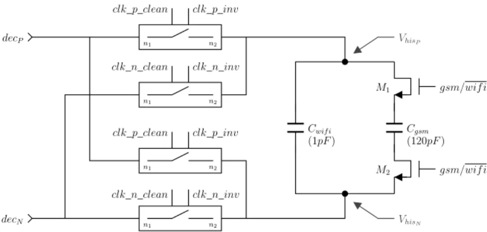
Filtre IIR
Le filtre IIR du premier ´etage analogique est constitu´e principalement d’une capacit´e histoire et de quatre switches (cf. Figure 8). Le filtre est identique pour les deux voies en quadrature I/Q, `a l’exception des signaux de commande qui sont d´ephas´es de π/2. Les deux filtres IIR sont connect´es aux nœuds communs decP et decN en sortie du LNTA (apr`es les capacit´es de d´ecouplage).
Cwif i Cgsm M2 M1 n1 n2 n1 n2 n1 n2 n1 n2 (1pF ) (120pF ) gsm/wif i gsm/wif i VhisN VhisP decP clk_p_inv clk_p_clean clk_n_clean clk_n_inv decN clk_n_clean clk_n_inv clk_p_inv clk_p_clean
Figure 8. Sch´ema du premier filtre IIR (voie I)
Les switches sont cadenc´es de sorte `a ce que chaque capacit´e histoire est retourn´ee `a une fr´equence 2Fc. La structure diff´erentielle du filtre et l’utilisation
de transistors factices (pour la r´ealisation des switches) permettent de minimiser la d´egradation li´ee aux ph´enom`enes d’injection de charges et de propagation des phases d’horloge.
La valeur de la capacit´e histoire est contrˆol´ee par le signal de commande gsm/wif i qui permet d’ajuster la r´ejection du filtre IIR en fonction du mode de fonctionnement du r´ecepteur.
Filtre anti-repliement
Comme d´ecrit pr´ec´edemment, les coefficients entiers du filtre anti-repliement ont ´et´e impl´ement´es au niveau circuit `a l’aide de rapports capacitifs. En suivant une approche hi´erarchique, le filtre peu ˆetre vu comme une combinaison de trois bancs de capacit´es, chacun compos´e de L cellules de coefficients, chacune d’elles ´
etant compos´ee de L cellules unitaires.
Le filtre anti-repliement a ´et´e dimensionn´e au tout d´ebut pour le mode GSM. Puis, des m´ecanismes de reconfiguration ont ´et´e rajout´es pour adapter la struc-ture au mode 802.11g. Notons qu’il est possible d’adapter le filtre `a d’autres standards de communication, mais la complexit´e de mise en œuvre et le nombre de signaux de contrˆole augmenterait de fa¸con drastique.
Le sch´ema ´electrique d’une cellule unitaire reconfigurable est donn´e Figure 9. Chaque cellule est compos´ee d’une capacit´e Ciet de trois switches correspondant
17 M1 Ci M3 M4 M2 Vcm
cellin cellout
(0.14 0.1) × 2 0.4 0.1 0.4 0.1 clkreset clkout 20f F node_Ci clkint gsm/wif i
Figure 9. Cellule unitaire reconfigurable du filtre SINC2
La valeur de la capacit´e unitaire a ´et´e calcul´ee lors de l’´etude syst`eme et permet d’obtenir le meilleur rapport gain/bruit du premier ´etage de traitement analogique. Les transistors des switches ont ´et´e dimensionn´es en fonction de la r´esistance Rsig calcul´ee ´egalement lors de l’´etude syst`eme. Des transistors
factices sont rajout´es afin de minimiser l’injection des charges sur la capacit´e unitaire Ci. La commande du switch d’int´egration est contrˆol´ee par le bit de
reconfiguration gsm/wif i et permet d’activer ou non la cellule unitaire en fonc-tion du mode de communicafonc-tion choisi.
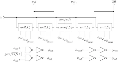
Les cellules unitaires sont organis´ees ensuite en cellules de coefficients, dont le sch´ema de principe est donn´e en Figure 10. Chaque coefficient est compos´e de L cellules unitaires (L = 5 en mode GSM) partageant une mˆeme entr´ee. Trois connexions diff´erentes sont possibles en sortie, selon si le coefficient garde le mˆeme signe (positif ou n´egatif) ou change de signe en fonction du mode de fonctionnement. Les connexions en sortie sont ´egalement g´er´ees `a ce niveau par le bit de contrˆole gsm/wif i.
unit Ci
φint
φout
φreset
unit Ci reconf Ci unit Ci unit Ci
φint φout φreset φint φout φreset φint φoutφ reset φint φoutφ reset in out gsm/wif i outx out kout gsm/wif i kout φout φout kout kreset φreset φout
Figure 10. Coefficient reconfigurable du filtre SINC2
18
voie I/Q, chacun de ces bancs ´etant constitu´es de 2L cellules de coefficients dont les connexions en entr´ee et sortie sont param´etrables. Le filtre anti-repliement SINC2 est reli´e au deuxi`eme ´etage de traitement analogique uniquement en mode GSM. En mode 802.11g, un filtrage IIR `a simple pole est rajout´e en sortie du filtre anti-repliement et le signal est ensuite amplifi´e puis connect´e `a une sortie du circuit.
Deuxi`
eme ´
etage DTASP
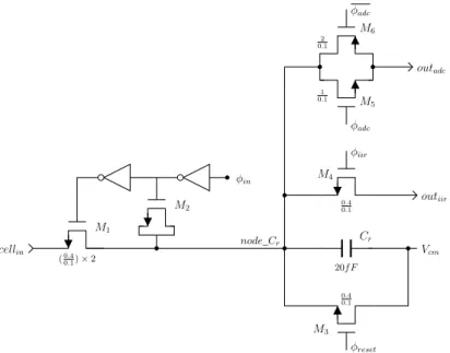
A l’image du premier ´etage de traitement analogique, le deuxi`eme ´etage DTASP comprend un filtre FIR r´ealisant un filtrage anti-repliement et une d´ecimation, ainsi qu’un filtre IIR r´ealisant une partie du filtrage canal. Le deuxi`eme filtre FIR est moins complexe que le filtre SINC2, puisqu’il s’agit d’impl´ementer des coefficients unitaires sous la forme [+1 -1 +1 -1]. La cellule unitaire utilis´ee `a ce niveau est repr´esent´ee Figure 11.
M1 M2 M3 Cr M4 M5 M6 cellin (0.4 0.1) × 2 φin node_Cr Vcm 0.4 0.1 outiir 20f F φreset φiir 0.4 0.1 outadc φadc φadc 1 0.1 2 0.1
Figure 11. Cellule unitaire du filtre FIR du second DTASP
Chaque capacit´e unitaire est connect´ee `a l’entr´ee du filtre FIR, puis `a la capacit´e histoire du filtre IIR, puis `a l’entr´ee de l’ADC et est enfin r´einitialis´ee avant le d´ebut de la phase suivante. La valeur de la capacit´e a ´et´e calcul´ee lors de l’´etude syst`eme (compromis entre perte de gain et bruit). Les r´esistances des divers switches d´ependent du temps allou´e `a chaque sous phase et de la constante de temps RC li´ee au transfert des charges.
Convertisseur analogique num´
erique
Le modulateur Σ∆ utilis´e en mode GSM pour la conversion du signal Fs/2 en
fin de chaine est repr´esent´e Figure 12. Le modulateur utilise un filtre de boucle passe haut de second ordre `a capacit´es commut´ees ainsi qu’un quantificateur `a
19
3 niveaux, et permet d’atteindre une r´esolution th´eorique de 12 bits pour une pleine ´echelle de 0.2 Vpp en diff´erentiel.
-+ z−1 +- z−1 1 −2 -in out
Figure 12. Architecture du modulateur Σ∆ utilis´e en mode GSM
Layout du circuit int´
egr´
e
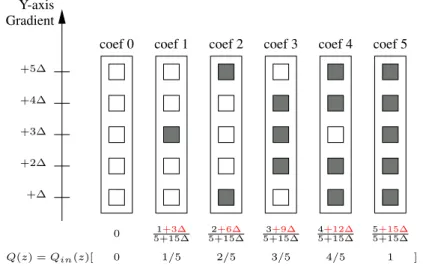
Le dessin des masques du filtre anti-repliement a ´et´e ´etudi´e avec attention afin de limiter les effets des disparit´es technologiques sur les performances en termes de filtrage. Il a ´et´e d´emontr´e que l’appariement des capacit´es unitaires ´etait n´ecessaire uniquement au niveau des cellules de coefficient, et non pas au niveau du filtre global.
coef 1 coef 2 coef 3 coef 4 coef 5 coef 0 +∆ +3∆ +4∆ +5∆ Y-axis Gradient +2∆ 0 1+3∆ 5+15∆ 4+12∆ 5+15∆ 5+15∆ 5+15∆ 2+6∆ 5+15∆ 3+9∆ 5+15∆ 1/5 0 Q(z) = Qin(z)[ 2/5 3/5 4/5 1 ]
Figure 13. Annulation du gradient au niveau des coefficients du filtre SINC2
Le placement des capacit´es unitaires a donc ´et´e r´ealis´e de sorte `a annuler tout gradient lin´eaire pouvant avoir lieu suivant un axe horizontal ou vertical, comme le montre la Figure 13. Notons ´egalement que l’annulation des gradients a ´et´e ´egalement ´etudi´ee au niveau sup´erieur du filtre anti-repliement, `a travers un placement optimal des cellules de coefficients le long de l’axe horizontal.
R´
esultats de mesures
Le front-end RF du r´ecepteur double mode propos´e, dont une micropho-tographie est donn´ee Figure 14, a ´et´e impl´ement´e et fabriqu´e en technologie
20
standard STMicroelectronics CMOS 90nm. La surface de la partie active du circuit est de 0.91mm2 et celle du circuit entier est de 2.5mm2. Le circuit a ´et´e
encapsul´e dans un boitier TQFP44L 44 broches.
ADC LNTA DCU FIR 2 AAF IIR 1 I Q
Figure 14. Microphotographie du r´ecepteur RF propos´e
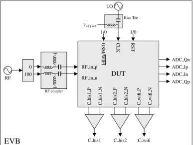
La carte d’´evaluation utilis´ee pour le test du circuit prototype est repr´esent´ee Figure 15. Le signal RF d’entr´ee est d’abord divis´e par un coupleur 0◦− 180◦,
puis achemin´e vers les entr´ees diff´erentielles du LNTA. Un r´eseau LC est utilis´e pour affiner l’adaptation d’imp´edance. Un second signal RF, `a une fr´equence 4Fc, est connect´e `a l’entr´ee horloge CLK du r´ecepteur. Le mode de
fonctionne-ment du circuit est contrˆol´e par un signal logique gsm/wif i.
C wifi P C wifi N C wifi C his2 P C his2 N C his2 ADC Ip ADC In ADC Qp ADC Qn C his1 P C his1 N C his1 CLK GSM/WIFI RST RF in p RF in n DUT 180 0
EVB
RF coupler Bias Tee 1/0 1/0 Vof f set RF LOFigure 15. Sch´ema de la carte d’´evaluation
L’´evaluation des ´etages de traitement analogiques `a temps discret est rendue possible grˆace aux signaux suivants :
21
– Vhis1,P et Vhis1,N : tension diff´erentielle aux bornes de la capacit´e histoire
du premier filtre IIR (voie I), disponible dans les deux modes GSM/802.11g – Vhis2,P et Vhis2,N : tension diff´erentielle aux bornes de la capacit´e histoire
du second filtre IIR (voie I), disponible uniquement en mode GSM – Vwif i,P et Vwif i,N : tension diff´erentielle en sortie du filtre anti-repliement
(voie I), disponible uniquement en mode 802.11g
Ces signaux sont analys´es `a l’aide d’oscilloscopes et/ou d’analyseurs de spectre. Les sorties num´eriques du modulateur Σ∆ sont analys´ees `a l’aide d’un analyseur logique et sont ´egalement utilis´ees pour l’´evaluation de la chaine de r´eception enti`ere.
Le plan de test suivant a ´et´e adopt´e pour la validation du fonctionnement et la mesure des performances du front-end RF propos´e. Toutes les mesures ont ´et´e effectu´e en mode GSM puis en mode 802.11g.
1. Phase de d´ebogue
2. Mesure de la consommation ´electrique
3. Gain du circuit en fonction de la fr´equence/puissance du signal d’entr´ee 4. R´ejection des filtres IIR & du filtre anti-repliement
La premi`ere s´erie de mesures effectu´ees sur le circuit ont prouv´e le bon fonctionnement du r´ecepteur et surtout la reconfiguration correcte du sch´ema de filtrage en fonction du mode de communication choisi. La consommation ´electrique des divers blocs analogiques et num´eriques est donn´ee en Tableau 3. Les valeurs obtenues en simulation et en mesures sur carte s’accordent parfai-tement.
GSM @ 3.6Ghz Voltage
Name
Pin 802.11g @ 4Ghz
measure simulation measure
9 vdd_ana_1 1.25 v 8 mA 7.4 mA 7.7 mA
22 vdd_dig_1 1.25 v 22 mA 23.4 mA 22.8 mA
23 vdd_LO 1.25 v 36 mA 24.7 mA 24.3 mA
26 vdd_dig_2 1.25 v 14 mA 16.4 mA
--27 vdd_ana2 1.25 v 43 µA 56 µA
--Tableau 3. Consommation ´electrique du front-end RF
Les r´esultats de simulations et de mesures concernant le gain en tension des divers blocs analogiques sont donn´es en Tableau 4. A l’exception d’une perte de gain inattendue en mode GSM, tous les autres r´esultats sont en quasi concordance.
DTASP2 SINC²
LNTA
Gain (dB) meas sim meas sim meas sim
GSM @945Mhz 34.6 37.4 N/A −1.83 −14.51 −2.28
N/A
WIFI @1.01Ghz 34.9 36.1 −0.12 −0.2
Tableau 4. Gain en tension des divers ´etages analogiques
La r´ejection des filtres IIR en mode GSM est donn´ee Figure 16. La r´ejection du second ´etage (Chist2) s’accorde avec les valeurs obtenues lors de l’´etude
syst`eme et suite aux simulations ´electriques du circuit.
La r´ejection du premier ´etage analogique est cependant moins ´elev´e que pr´evu, ce qui pourrait ˆetre caus´e par des valeurs de capacit´es parasites bien plus ´elev´ees que celles estim´ees par l’extracteur post layout.
22
Figure 16. R´ejection des filtres IIR en mode GSM
Conclusion
La premi`ere partie de la th`ese a ´et´e consacr´ee `a la revue des architectures de r´eception radio les plus couramment utilis´ees dans les syst`emes de communica-tion sans fil, en mettant l’accent sur les aspects de reconfiguracommunica-tion, int´egration et de faible consommation). Dans le cadre de la Radio Logicielle, les r´ecepteurs `a ´
echantillonnage RF et les techniques de traitement de signal analogique `a temps discret sont de plus en plus utilis´es.
Le premier objectif de cette th`ese a ´et´e d’´etudier et de proposer une archi-tecture de r´eception reconfigurable architecture bas´ee sur les concepts ci-dessus. Un r´ecepteur RF temps discret `a ´echantillonnage RF a ´et´e effectivement propos´e et mis en œuvre en technologie CMOS 90nm. Les normes GSM900 et 802.11g ont ´et´e choisies comme cibles pour l’´etude syst`eme et la validation de la recon-figurabilit´e du r´ecepteur (diff´erents plans de fr´equences et syst`emes de filtrage ont ´et´e adopt´es pour chaque norme). Le r´ecepteur est compos´e d’un LNA `a transconductance, deux ´etages de traitement de signal analogique `a temps dis-cret pour la translation en fr´equences, le filtrage anti-repliement, la d´ecimation et une partie du filtrage canal. En changeant le taux d’´echantillonnage ainsi que certains param`etres au niveau du circuit, il a ´et´e possible d’adapter le r´ecepteur RF `a diff´erentes bandes RF et d’adapter le filtrage en fonction des sp´ecifications exig´ees par chaque norme.
Le deuxi`eme objectif de la th`ese ´etait d’´etudier le probl`eme de repliement de spectre, propre aux architectures `a sous-´echantillonnage et de trouver de nouveaux sch´emas de filtrages plus performants, compl`etement reconfigurables et `a faible consommation ´electrique. Dans ce cadre, un filtre anti-repliement `a temps discret de second ordre en SINC2 a ´et´e propos´e et impl´ement´e dans le r´ecepteur RF. Bas´e principalement sur des matrices de capacit´es commut´ees, ce filtre permet d’obtenir une r´ejection assez ´elev´e et pr´esente l’avantage d’ˆetre totalement reconfigurable, et donc parfaitement adapt´e aux applications multi-standards.
23
Les premi`eres s´eries de mesures effectu´ees sur le circuit prototype ont per-mis de d´emontrer le bon fonctionnement du r´ecepteur. La conception d’une carte de test d´edi´ee est cependant n´ecessaire afin de continuer la validation du r´ecepteur et d’estimer les performances en terme de gain et de filtrage. Plu-sieurs am´eliorations pourraient ˆetre apport´ees au circuit actuel, afin notamment de r´eduire la consommation ´electrique et d’augmenter le nombre de standards pouvant ˆetre adress´es.
Symbols and Abbreviations
1/f Flicker noise
αk Filter tap coefficient
φk k-th sampling phase µ Carrier mobility σ Standard deviation ∆ Process gradient CB Buffer capacitor CH History capacitor CR Rotating capacitor
Cpar Parasitic capacitance
Cox Gate oxide capacitance
Fc Channel frequency Fs Sampling frequency Gm Transconductance H(z) Transfer function M Decimation ratio S(f ) Spectral density Ti Integration period Ts Sampling period V (t) Voltage signal Vcc Supply voltage VT H Threshold voltage
AAF Anti-alias filer
ADC Analog to digital converter
CMOS Complementary metal oxide semiconductor
DAC Digital to analog converter
DCU Digital control unit
DTASP Discrete time analog signal processing
FFT Fast Fourier Transform
FIR Finite impulse response
GSM Global system for mobile communications
I/Q In-phase/Quadrature
IF Intermediate frequency
IIR Infinite impulse response
LNA Low noise amplifier
26
LO Local oscillator
NF Noise figure
PSD Power spectrum density
RF Radio frequency
SAW Surface acoustic wave
SDR Software defined radio
SINC Sinus cardinal
Contents
1 Introduction 35
2 Overview of wireless receiver architectures 37
2.1 Introduction. . . 37 2.2 Overview of receiver architectures. . . 37 2.2.1 Superheterodyne receiver . . . 38 2.2.2 Direct conversion receiver . . . 39 2.2.3 Low-IF receiver . . . 40 2.3 Software defined radio . . . 41 2.3.1 Ideal SDR architecture. . . 42 2.3.2 Hardware requirements . . . 43 2.4 Multi-standard receivers . . . 43 2.4.1 Previous realizations . . . 44 2.4.2 RF sampling architecture . . . 45 2.5 Conclusion . . . 45
3 Study of the RF sampling receiver 47
3.1 Introduction. . . 47 3.2 Bandpass sampling . . . 47 3.2.1 Basics of bandpass sampling. . . 48 3.2.2 Problems of subsampling . . . 49 3.3 Charge sampling . . . 51 3.3.1 Elementary charge sampling circuit. . . 51 3.3.2 Elaborated charge sampling structures . . . 53 3.4 State-of-the-art realizations . . . 55 3.4.1 RF sampling receivers . . . 55 3.4.2 Charge sampling circuits. . . 58 3.4.3 Anti-alias filtering . . . 58 3.5 Conclusion . . . 59
4 Proposed receiver architecture 61
4.1 Introduction. . . 61 4.2 Targeted standards . . . 61 4.2.1 GSM specifications . . . 62 4.2.2 802.11g specifications . . . 63 4.2.3 Scaled-down version of 802.11g . . . 65 4.3 Architecture overview . . . 65 4.3.1 RF stage . . . 65
28 CONTENTS
4.3.2 First DTASP stage . . . 66 4.3.3 Second DTASP stage . . . 67 4.3.4 A/D conversion. . . 68 4.4 Frequency plan . . . 68 4.4.1 GSM mode . . . 68 4.4.2 802.11g mode . . . 69 4.5 Second order anti-alias filter . . . 70 4.5.1 Principle . . . 70 4.5.2 Coefficient implementation . . . 72 4.5.3 Rejection estimation . . . 74 4.6 Receiver system design . . . 75 4.6.1 Design guidelines . . . 75 4.6.2 System level description . . . 76 4.6.3 Gain/Noise analysis . . . 78 4.6.4 Filtering requirements . . . 83 4.7 Conclusion . . . 84
5 Receiver front-end design 87
5.1 Introduction. . . 87 5.2 RF section. . . 87 5.2.1 RF filter. . . 87 5.2.2 Transconductance LNA . . . 89 5.3 First IIR filter . . . 91 5.3.1 History capacitor switches . . . 91 5.3.2 Clock buffers . . . 93 5.3.3 Reconfigurability . . . 94 5.3.4 Output buffers . . . 94 5.4 Anti-alias filter . . . 95 5.4.1 Unit cell . . . 95 5.4.2 Coefficient cell . . . 96 5.4.3 Capacitor bank . . . 98 5.4.4 Top view . . . 100 5.5 Second DTASP block. . . 100 5.5.1 Unit cell . . . 101 5.5.2 Top view . . . 101 5.6 Digital Control Unit . . . 102 5.6.1 D flip-flop cell. . . 103 5.6.2 Clock phases generation . . . 103 5.6.3 DCU reconfigurability . . . 105 5.6.4 LO input buffer. . . 106 5.6.5 Simulated performances . . . 107 5.7 A/D converter . . . 109 5.8 Layout considerations . . . 110 5.8.1 Capacitor layout . . . 110 5.8.2 Gradient cancellation techniques . . . 112 5.9 Conclusion . . . 114
CONTENTS 29
6 Experimental results 115
6.1 Introduction. . . 115 6.2 DUT and bench description . . . 115 6.2.1 Chip layout and packaging . . . 115 6.2.2 Evaluation board description . . . 116 6.2.3 Validation plan overview. . . 117 6.2.4 Notes on ADC analysis . . . 117 6.3 Measurement results . . . 118 6.3.1 Debug phase . . . 118 6.3.2 Gain evaluation . . . 119 6.3.3 Filtering evaluation . . . 122 6.4 Conclusion . . . 122 7 Conclusion 123 A Scilab code 125 B Noise analysis 133 Bibliography 142
List of Figures
2.1 Superheterodyne receiver architecture . . . 38 2.2 Homodyne receiver architecture . . . 39 2.3 Low-IF receiver architecture . . . 41 2.4 Ideal software defined radio architecture . . . 42 2.5 Multi-standard receiver using zero-IF architecture . . . 44 2.6 RF sampling receiver architecture. . . 45
3.1 Spectra of bandpass sampling . . . 48 3.2 Permissible zones for uniform sampling without aliasing . . . 49 3.3 Illustration of effective noise bandwidth . . . 50 3.4 Noise aliasing due to subsampling. . . 51 3.5 Active charge sampling circuit. . . 52 3.6 Magnitude responses of voltage and charge sampling circuits . . 53 3.7 Time interleaved charge sampling . . . 54 3.8 Charge sampling with embedded FIR filtering . . . 54 3.9 TI’s first discrete-time RF sampling receiver. . . 56 3.10 Jakonis’s RF sampling receiver front-end . . . 56 3.11 Abidi’s discrete-time RF sampling receiver . . . 57 3.12 STMicroelectronics Fs/2 discrete-time sampling receiver . . . 57
4.1 Blocking profile for GSM 900 . . . 62 4.2 802.11g European operating channels. . . 63 4.3 802.11g adjacent channel rejection . . . 64 4.4 Proposed receiver architecture. . . 66 4.5 Fractioned operation of the 1st DTASP block . . . . 66 4.6 Spectrum folding during first sampling . . . 67 4.7 GSM mode frequency plan. . . 68 4.8 WIFI mode frequency plan . . . 69 4.9 Notch placement in anti-alias filtering . . . 71 4.10 Coefficient implementation through charge division . . . 72 4.11 Arrangement of parallel integration paths in GSM mode . . . 73 4.12 Timing diagram for interleaved AAF operation . . . 73 4.13 Notch degradation due to circuit level mismatches . . . 74 4.14 Circuit parameters to be specified at system level . . . 76 4.15 Simplified circuit schematic for system analysis . . . 77 4.16 Noise at LNTA and IIR stage . . . 79 4.17 Equivalent schematic of the AAF stage. . . 80 4.18 Input of the second DTASP stage . . . 81
32 LIST OF FIGURES
4.19 Output of the second DTASP stage. . . 82 4.20 Signal and noise levels in GSM mode . . . 83 4.21 ADC input dynamic range partitioning in GSM mode . . . 83 4.22 Blocker & Adjacent levels in GSM mode . . . 84
5.1 SAW filter transfer function in GSM mode. . . 88 5.2 Schematic of the LNA transconductance stage. . . 89 5.3 Schematic of the common mode feedback control . . . 90 5.4 Ideal modelling of the LNTA . . . 90 5.5 Schematic of the first IIR stage (I path) . . . 91 5.6 Schematic of the history capacitor switch . . . 92 5.7 Parasitic capacitors of the IIR filter switches . . . 92 5.8 Buffering of the IIR clock phases . . . 93 5.9 Output buffer . . . 94 5.10 Schematic of the SINC2 unit cell . . . 95 5.11 Schematic of the SINC2 reconfigurable unit cell . . . 96 5.12 Example of a SINC2 coefficient cell (coef 14) . . . 97 5.13 Reconfigurable SINC2 coefficient cell . . . 97 5.14 Arrangement of SINC2 coefficients into bank . . . 99 5.15 Top view of the anti-alias filter . . . 100 5.16 Schematic of the FIR2 unit cell . . . 101 5.17 Top view of the 2nd DTASP block . . . 102 5.18 Schematic of the D flip-flop . . . 103 5.19 Generation of the history capacitors clock phases . . . 104 5.20 Improved version of the token ring . . . 104 5.21 Design concept for clock phases generation. . . 105 5.22 Reconfiguration of the token ring using pass gates . . . 106 5.23 Buffering of the input clock signal . . . 106 5.24 Timing diagram of the entire clock phases in GSM mode . . . 108 5.25 Architecture of the Σ∆ modulator . . . 109 5.26 Schematic of the Σ∆ ADC. . . 110 5.27 Unit capacitor layout. . . 111 5.28 History capacitor layout . . . 111 5.29 Gradient cancellation within AAF coefficients . . . 113 5.30 Gradient cancellation at AAF top level . . . 114
6.1 Chip microphotograph of the proposed discrete-time receiver . . 116 6.2 Evaluation board synaptic . . . 117 6.3 Gain versus RF input frequency (GSM mode) . . . 119 6.4 Gain versus RF input frequency (802.11g mode) . . . 120 6.5 Gain versus RF input level (GSM mode). . . 121 6.6 Gain versus RF input level (802.11g mode) . . . 121 6.7 IIR filters response in GSM mode. . . 122
B.1 Thermal noise sources in a coefficient cell . . . 133 B.2 Equivalent circuit for the integration switch noise contribution . 134 B.3 Noise model for the output of the 1st DTASP stage. . . 135 B.4 Noise sources through the 2nd DTASP stage. . . 136
List of Tables
4.1 GSM sensitivity and signal levels . . . 62 4.2 GSM adjacent channel selectivity . . . 63 4.3 802.11g sensitivity and signal levels. . . 64 4.4 FIR filter coefficients for GSM and WIFI modes . . . 71 4.5 FIR coefficients in distinct zeros configuration . . . 72 4.6 Gain and noise contributions in GSM mode . . . 82 4.7 Blocker & Adjacent levels in GSM mode . . . 84
5.1 Characteristics of the GSM mode SAW filter . . . 88 5.2 SAW filter characteristics in WIFI mode . . . 89 5.3 Test conditions for evaluating the DCU performances. . . 107 5.4 Maximum operating range of the DCU. . . 107
6.1 Voltage supply current consumption . . . 119 6.2 Voltage gain at intermediate stages . . . 120
Chapter 1
Introduction
Motivation and aim of the research
Recent trends in cellular radio terminals towards smaller handsets, and the proliferation of radio standards around the world place many demands on the future of radio terminals. Software Defined Radio (SDR) is an enabling technol-ogy which may provide a solution for the realisation of multiband, multimode radio terminals by defining radio functionality in software [36]. This allows the radio terminal to be adapted to different systems or customised for various services by reprogramming the radio functionality.
A possible solution for increasing both the receiver integration level and re-configurability is to transfer the signal sampling and analogue-to-digital (A/D) interface from the baseband to higher frequencies, i.e. to an IF, or optimally directly to RF, and to use a high-speed A/D converter to enable further signal processing to take place in the digital domain. As an inherent advantage, digital signal processing allows elimination of the non-idealities of analogue signal pro-cessing, such as device noise and non-linearities, and of component mismatches. Technological progress towards diminished transistor feature size, especially in pure CMOS processes, also favours an increased level of digital signal process-ing in receiver implementation[44]. A fully software-defined radio [8], and even a partially programmable radio supporting multiple wireless standards would directly benefit from radio architectures based mostly on digital signal process-ing and digital controllability. However, usprocess-ing an architecture based on a high resolution bandpass A/D converter at a high frequency imposes very demanding requirements on the dynamic range of the converter and results in an increased overall power consumption.
Instead of directly converting a high frequency RF signal into digital form, bandpass sampling can be used to perform frequency downconversion prior to A/D conversion. This helps decreasing the overall power dissipation and allows the use of discrete-time digital signal processing techniques (in an analog im-plementation) to achieve a high integrability in an advanced CMOS technology. It has proved difficult, however, to realize the required appropriate bandpass anti-alias filtering and obtain adequate noise performance in high-frequency op-eration with elementary implementations of subsampling circuits [11].
36 Introduction
investigate and implement a reconfigurable architecture for a multi-standard receiver [32], based on the concepts of RF bandpass sampling and discrete-time analog signal processing. Although several implementations of such discrete-time receivers have already been reported [14, 42], only few of them have tried to target different communication standards in order to truly validate the multi-standard capability [4,39]. In the current work, a reconfigurable discrete-time receiver based on RF sampling is actually proposed. The GSM900 and 802.11g standards (which have very different specifications and requirements) are chosen as target standards to validate the implemented reconfiguration mechanisms and hence the reconfigurability of the receiver.
The second aim of the thesis is to study and propose new solutions for enhanced anti-alias filtering. A fully passive second order sinc-type anti-alias filter [33] is analyzed in the current work and implemented in the proposed RF sampling receiver. Basically, the filter is constructed as a discrete-time FIR filter with tap coefficients implemented through capacitive ratios. In addition to offering an improved alias rejection, the proposed filter does not result in power consumption increase and is above all adapted for multi-standard receiver operations.
Organisation of the thesis
The thesis is organized as follows. A short review of wireless receiver archi-tectures is presented in Chapter 2. The concept of Software Defined Radio is introduced and some of the best architecture candidates for multi-standard re-ceivers are described. The discrete-time RF sampling receiver and the principle of frequency downconversion by subsampling are presented in Chapter 3. This chapter also presents the fundamentals of charge-domain sampling and describes how this technique can be utilized to implement anti-aliasing and elementary filtering functions in discrete-time RF sampling receivers. Chapter 4 presents the proposed reconfigurable receiver with its main innovations (dual-mode oper-ation and improved anti-alias filtering) and details the system level study of the architecture. Chapter 5 details the circuit level design of the circuit and points out the major circuit problems encountered during the design of discrete-time receivers. Chapter 6 presents preliminary results of measurements performed on the implemented prototype circuit. A summary of thesis work and perspectives for future work are finally presented in conclusion.
Major contributions
- Discrete-time RF sampling receiver in CMOS technology
- GSM and 802.11g dual-mode reconfigurable receiver architecture - Second order discrete-time anti-alias filter with improved rejection - System level study and noise analysis of discrete-time receivers
Chapter 2
Overview of wireless
receiver architectures
2.1
Introduction
This chapter offers a review of the radio receiver architectures that are the most widely used in today’s wireless communications systems. The advantages of these architectures are discussed in terms of performance, suitability for in-tegration and also in terms of reconfigurability and multi-standard capability. The concept of Software Defined Radio is then introduced and some of the hardware requirements that are imposed on the RF front-end part are pre-sented. The multi-standard concept which is leading the path towards software defined radios is then addressed and some of the best candidate architectures for multi-standard radios are finally presented.
2.2
Overview of receiver architectures
When developing and designing RF receiver for a wireless mobile communica-tion system, designers first determine what type of architecture will be employed based on requirements of performance, cost, power consumption, and robust im-plementation. This section present the architectures of the RF receivers that are practically applicable to the mobile stations of wireless communication systems. RF front-end receivers are defined from the antenna to the analog to digital converter and are usually formed by different devices and circuits operating at radio frequency (RF) band, intermediate frequency band (IF) and analog baseband. The Analog to Digital converter (ADC) is often used as a boundary between the RF receiver and its digital counterpart. However, this boundary is getting ambiguous with the state of the art of ADCs running at higher and higher sampling rates, in which case, the ADC will be certainly also considered as part of the RF receivers [12].
At present most RF transceivers in wireless communication systems are using the superheterodyne architecture. This architecture has the best performance if compared with the others, and therefore it has been the most popular transceiver architecture since it was invented in the 1910s [12]. Capable of multi-mode
oper-38 Overview of wireless receiver architectures
ations with great cost saving and no increasing extra parts, the direct conversion or homodyne architecture has emerged and became a very popular radio archi-tecture for wireless mobile communication systems. To overcome some issues of direct conversion architecture, a modified architecture referred to as low IF ar-chitecture was then created. Some wireless communication receivers especially based on the CMOS technology started to employ this architecture to cope with the flicker noise and the DC offset problems of the direct conversion. Following this same order, this section will first discuss the superheterodyne architecture, then the direct conversion (zero-IF) and low-IF architectures.
2.2.1
Superheterodyne receiver
The superheterodyne architecture is probably the most commonly employed in current wireless systems. It consists in mixing an incoming signal with an offset frequency local oscillator (LO) to generate an intermediate frequency (IF) signal in the receiver case. In a superheterodyne transceiver, the frequency translation process may be performed more than once, and thus it may have multiple intermediate frequencies and multiple IF blocks. The superheterodyne architecture that is based on a two-stage downconversion scheme (dual-IF) is the most used in today’s RF receivers (illustrated in Fig.2.1).
IF RF Antenna BPF Amplifier IRF LO LO BPF BPF Amplifier
Figure 2.1: Superheterodyne receiver architecture
The out-of-band blocking signals are reduced by an RF bandpass filter placed immediately after the antenna. The signal is then amplified by an LNA, which must have a sufficiently low noise to allow detection of weak signals but must also have the dynamic range to handle in-band interferers. The bandpass filter is usually insufficient to reduce signals at the image frequency to the system noise level, and so a second image filter is inserted prior to mixing. To ensure that the image is sufficiently far away from the wanted signal to allow effective filtering, a relatively high first intermediate frequency must be chosen (for 1 to 2 GHz RF systems an IF of 100-200 MHz is common).
The mixer must still handle the complete dynamic range of the in-band signal. After the mixer, a SAW filter can be used to achieve the channel filtering. At these frequencies the SAW filter is small but usually has a large in-band loss
2.2 Overview of receiver architectures 39
when complete channel filtering is to be achieved. The output drive of the mixer must therefore boost the signal level to allow for this loss.
Once the interfering channels have been attenuated, the signal is boosted to a high level (it can be limited if a constant-amplitude modulation scheme is used). The signal is then reduced to baseband frequency for demodulation. It is of course possible to split the channel filtering between the two intermediate frequencies. This will require a greater dynamic range in the second mixer.
This architecture requires the synthesis of two local oscillators, and their frequencies must be chosen so that spurious responses from the radio are kept to a minimum. This aspect of frequency planning, which will not be discussed in more detail here, is a well-understood design process which requires considerable care and experience.
This design requires several external filters and therefore does not lend itself to easy integration as the pin count increases. Moreover, the filters are usually single ended and hence achieving isolation between pins becomes an issue. In particular, the channel filter will often need to provide 50 dB of attenuation at key frequencies, thus implying that greater isolation must be achieved between the pins and with respect to signal ground if the filter response is not to be degraded. The image filter can be eliminated if an image-rejecting mixer is used. This will prevent the need to come off chip after the LNA and makes an LNA plus image-reject mixer a useful integrated building block.
2.2.2
Direct conversion receiver
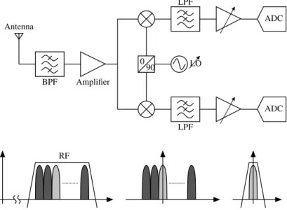
Direct conversion receivers are widely listed and documented in the literature [3, 50] . Direct conversion means that the RF signal is directly downconverted to baseband without intermediate frequency stages, and therefore it is also referred to as zero-IF. The direct conversion architecture (illustrated in Fig. 2.2) has many attractive features and offer the best opportunity for integrated systems because of its simplicity.
RF ADC ADC Antenna BPF Amplifier LO LPF LPF 0 90
40 Overview of wireless receiver architectures
Once again, an RF bandpass filter is placed at the input. The LNA’s output is passed into the mixer. The LNA must handle the same dynamic range as for the superheterodyne architecture and it must have enough gain to lift weak signals above the noise of the mixer. The mixer however, now converts directly to baseband. Thus the signal is its own image, and channel filtering can now be carried out by low-pass baseband filters. Only one local-oscillator frequency needs to be synthesised, and frequency planning is straightforward. Moreover, the expensive IF passive filter (SAW filter) can now be eliminated, and then the cost and size of the overall transceiver are reduced.
The channel filtering of the direct conversion receiver is performed at base-band using an active lowpass filter. The base-bandwidth of the active filter can be designed as adjustable. Thus, it is easy to design the direct conversion receiver for multi-mode operations with a common analog baseband circuitry and even a common RF front-end.
The configuration of the direct conversion radio may seem simpler than that of the superheterodyne radio, but its implementation is much more difficult since there are a number of technical challenges in the direct conversion receiver [12]. The main issue is associated with DC signals which are generated by imper-fections in the mixer. These signals are implicitly in-band and it is therefore difficult to filter them from the wanted signal. It is necessary to keep them suf-ficiently below the signal. Unfortunately, the amplification that can be applied to the signal before mixing is limited by the level of in-band interferers which must not overload the mixer.
The main issue is associated with DC offsets that arise from many sources. Imbalance in the mixers will lead to a DC output. This is generally a constant quantity and could be cancelled with suitable circuitry. Any leakage of the local oscillator to the input of the receiver will also result in a DC signal being gen-erated. If this leakage is via radiation coupling into the antenna, then this may vary with the local environment. Finally, non-linearities in the mixer may cause signals to be generated at DC from other interferers. The latter mechanisms can be time varying, and any offset cancellation needs to be able to respond to time variation. It is only when special precautions are taken to cancel DC offsets that direct-conversion architectures can be used.
I/Q mismatches are other associated problems due to the quadrature down-conversion in homodyne receivers. Because the down-converted signal is located at zero frequency, flicker noise or 1/f noise of devices will also corrupt the information signal. More details of the direct-conversion issues are given in [50].
2.2.3
Low-IF receiver
The low-IF receiver (illustrated in Fig. 2.3) combine the advantage of both superheterodyne and homodyne receivers [55]. The received RF signal is down-converted to IF by an LO, where the intermediate frequency can be as low as half to two times the bandwidth of the desired signal. The main advantage of the low IF architecture over the direct conversion one is that this architecture has no DC offset problem because the desired signal is off the DC by the IF.
Properly choosing the low IF can remove the low frequency interference product that results from AM demodulated out of band interferers (due to second order nonlinearities). In addition, the low IF architecture is also able to significantly reduce the near DC flicker noise impact on the receiver performance.
2.3 Software defined radio 41 ADC ADC IF RF LO LPF LPF 0 90 Amplifier BPF Antenna sin(2πfLO2t) cos(2πfLO2t) cos(2πfLO2t)
Figure 2.3: Low-IF receiver architecture
This architecture, thus, is quite attractive for the highly integrated transceivers based on the CMOS technology (which is more concerned by the flicker noise than other technologies such GaAs).
The main issue of the low IF receiver architecture is the image problem, since the IF is too low to separate the image from the desired signal by means of a bandpass filter in the RF stage. The imbalance between I and Q channel signals in the low IF receiver determines the possible maximum image rejec-tion. To achieve high image rejection, it is necessary to minimize the imbalance of the I and Q signals by means of complex quadrature downconversion [56] or by a combination of the quadrature downconversion and complex bandpass filtering [21].
A generic wideband receiver evolved from the conventional receiver architec-ture, shown in Fig.2.3, has been used in cellular phone base stations to support multiple wireless communication standards and to meet the rapidly increasing demands of cellular services [71]. In this application, multiple channels at the RF are selected by the first tunable LO instead of a single channel in super-heterodyne receivers. All the selected channels are translated to baseband by the second LO with a fixed frequency and then digitized in a wideband A/D converter for I and Q components respectively [34,35, 53]. The number of si-multaneous channels that can be received would be limited by the digital signal processing capability.
2.3
Software defined radio
A software defined radio (SDR) [6,38] is a form of transceiver in which ideally all aspects of its operation are determined using versatile, general-purpose hardware whose configuration is under software control [31]. The concept of software defined radio was originally conceived for military applications. It consists of a single radio receiver to communicate with different types of military radios using different frequency bands and modulation schemes. This concept is starting to be introduced into commercial applications.
42 Overview of wireless receiver architectures
As technology progresses, an SDR can move to an almost total SR, where the digitization is at (or very near to) the antenna and all of the processing required for the radio is performed by software running on high-speed digital signal processing elements [61]. The ideal case is doing sampling and digitization directly on an RF signal. Due to the presence of strong interferers around weak RF information signal, an A/D converter with a higher dynamic range up to around 100 dB might be needed. However, it is hard to achieve by current A/D converter technology.
2.3.1
Ideal SDR architecture
A possible architecture for an ideal software defined radio [31] is shown in Fig2.4. Note that the A/D converter is assumed to have a built-in anti-alias filter and that the D/A is assumed to have a built-in reconstruction filter.
D / A A / D DSP RF−output DAC RF−input ADC subsystem Digital processing High−linearity high−efficiency wideband RF PA circulatorIdeal Transmit/Receive antenna
Figure 2.4: Ideal software defined radio architecture
The ideal software defined radio has the following features [31]:
- The modulation scheme, channelisation, protocols, and equalisation for transmit and receive are all determined in software within the digital pro-cessing subsystem.
- The ideal circulator is used to separate the transmit and receive path signals, without the usual frequency restrictions placed upon this func-tion when using filter based solufunc-tions. This component relies on perfect matching between itself, the antenna and power amplifier impedances and so is unrealistic in practice (based upon typical transmit/receive isolation requirements). Since duplexers are usually fixed frequency components, their elimination is a key element in a multi-band or even multi-standard radio. Note that the circulator would also have to be very broadband, which most current designs are not.
2.4 Multi-standard receivers 43
- The linear (or linearised) power amplifier ensures an ideal transfer of the RF modulation from the DAC to a high-power signal suitable for trans-mission, with low adjacent channel emissions. Note that this function could also be provided by an RF synthesis technique, in which case the DAC and power amplifier functions would effectively be combined into a single high power RF synthesis block.
- Anti-alias and reconstruction filtering is clearly required in this archi-tecture. It should be, however, relatively straightforward to implement, assuming that the ADC and DAC have sampling rates of many gigahertz. Current transmit, receive, and duplex filtering can achieve excellent roll-off rates in both cellular and base station designs. The main change would be in transforming them from bandpass (where relevant) to lowpass designs.
2.3.2
Hardware requirements
The ideal hardware architecture, shown in Fig.2.4, imposes some difficult spec-ifications upon each of the elements in the system. Some of these specspec-ifications can be summarised as follows [31]:
1. Antenna: A frequency range of almost 5 octaves is required, together with a realistic gain/loss figure around 0 dBi. Combined with the handset requirements of small size, omnidirectional coverage and low cost, the physical realization of this component becomes extremely challenging. 2. Circulator or duplexer:A high isolation and a broadband coverage range
are needed. In the case of a conventional, filter-based duplexer, this latter requirement is impossible to achieve with current technologies.
3. A/D converter: The sampling rate of the converter, if Nyquist sampling directly at RF, would need to be at least 4.4 GHz and, in reality, much more (to allow for a realistic anti-alias filter roll-off). This is an extremely hard specification, particularly with current technology.
4. Receiver anti-alias filtering: Based on the two-times Nyquist sampling converters discussed above, an attenuation of 60 dB is required around 18 MHz from the channel edge. This would be extremely difficult, if not impossible, to achieve in a bandpass filter capable of tuning from 100 MHz to 2.2 GHz. Improvements in sampling rates (for a given converter resolu-tion) will, however, allow this requirement to be relaxed and may enable some limited forms of SDR to be realised without such high performance filtering needing to be included.
The specifications outlined here and the components required to realise them are clearly not available with current technology and may not be achievable, in many cases, for a considerable period.
2.4
Multi-standard receivers
As previously mentioned, software defined radios are still not feasible today due to technology limitations and it is hence more reasonable to speak about
![Figure 2.4: Ideal software defined radio architecture The ideal software defined radio has the following features [31]:](https://thumb-eu.123doks.com/thumbv2/123doknet/11457370.290990/43.892.230.731.457.777/figure-software-defined-architecture-software-defined-following-features.webp)