Design of a 4x4 Bidirectional Routing Board
by
Victor Ernest Chin
Submitted to the Department of Electrical Engineering and
Computer Science
in partial fulfillment of the requirements for the degree of
Master of Engineering in Electrical Engineering and Computer
Science
at the
MASSACHUSETTS INSTITUTE OF TECHNOLOGY
August 1995
( Victor Ernest Chin, MCMXCV. All rights reserved.
The author hereby grants to MIT permission to reproduce and
distribute publicly paper and electronic copies of this thesis
document in whole or in part, and to grant others the right to do so.
Author
...
Department of Electrical Engineering and Computer Science
August 15, 1995 / ir
I I
!Certified by.
Y,
Accepted by
George A. Boughton
Research Associate
Thesis Supervisor
A"ark
" ~~,~
',,I v
...
is
F. R. Morgenthaler
Chairman, Department
omittee
on Graduate Theses
CF 29'r' -:Ci',)G'y
JAN 29 L996
Design of a 4x4 Bidirectional Routing Board
by
Victor Ernest Chin
Submitted to the Department of Electrical Engineering and Computer Science
on August 15, 1995, in partial fulfillment of the
requirements for the degree of
Master of Engineering in Electrical Engineering and Computer Science
Abstract
The 4x4 bidirectional routing board is the primary building block for the message passing network used in StarT-NG, a message passing machine with support for shared memory being developed at the Laboratory for Computer Science at MIT. The board uses Arctic chips, 4x4 unidirectional packet routing chips, to implement a fat tree network. These boards can be interconnected through a backplane to create a larger fat tree network, like a 16x16 bidirectional or 32x32 bidirectional fat tree network. In addition to implementing the network, the board includes the link technology necessary to transmit and receive data over long cabling to either another node in the tree or to a processor, and insures the proper handling of JTAG signals for control and testing of the Arctic chips.
Thesis Supervisor: George A. Boughton Title: Research Associate
Acknowledgments
I would like to thank George (Andy) Boughton for the concepts and design sugges-tions. I would like to thank Dan Rosenband for his suggessugges-tions. Finally, I would like to thank Jack Constanza for his contributions which aided in the design
Contents
1 Introduction
1.1 Arctic and JTAG Signals ...
1.1.1 Arctic Chip . . . .
1.1.2 JTAG Signals ...
1.2 4x4 Bidirectional Board Setup 1.2.1 Arctic Network ....
1.2.2 GTL/ECL Converter .
1.3 Thesis Outline ...
2 ECL Links
2.1 Voltage Level Translation ....
2.2 ECL Link Transmission ...
2.2.1 Hardware ...
2.2.2 Timing ...
2.3 ECL Link Reception ...
2.3.1 Hardware ...
2.3.2 Timing ...
3 JTAG Signals
3.1 4x4 Routing Board Requirements 3.2 Voltage Translation ... 3.3 Timing Requirements ... 8 8 9 10 10 11 11 12 14 ... ...15 ... ...17
. .... .. ... .. ... .. ... ...
17
... ...18 ... ...18 ... ...18 , ... . . . 19 20 20 22 24 . . . . . . . . . . . . . . . . . . . . . . . . . . . . . . . . . . . . . . . . . . . . . . . . . . . . . . . . . . . . . . . . . . . . . . . ....
...
...
4 Power and Area 27
4.1 Power ... 27
4.2 Area ... 28
5 Conclusion 30 5.1 Other Board Design Issues . . . ... 30
5.2 Possible Testing Procedures . . . .... 32
A Tables 33 B Figures 36 C Calculations 40 C.1 ECL Transmission ... 40 C.2 ECL Reception ... 41 C.3 JTAG Signals ... 42
C.3.1 Clocking tdi and tms . . . .... 42
List of Figures
Actic Chip ...
4x4 Routing Board Sections . . 4x4 Arctic Network ...
4x4 Arctic Output Timing . . Voltage Translation ...
4x4 Arctic Receiver Timing tclk Termination on 4x4 Board
Voltage Translation Diagram . PC Board tdo Termination . . .
JTAG Signals' Timing ... GTL to ECL Conversion .... ECL to GTL Conversion .... 4x4 Board Initial Layout ....
9 11 12 1-1 1-2 1-3 2-1 2-2 2-3 3-1 3-2 3-3 3-4 B-1 B-2 B-3 . . . .... . . . 14 . . . .... . . . 16 . . . .... . . . 19
... . .21
. . . 22 . . . .24 . . . 25 37 38 39...
...
...
...
... I...
...
...
...
List of Tables
AMCC PLL Phase Selections AMCC PLL Phase Resolution Device Power ...
Termination Power ...
4x4 Board Component Listing ECL Transmission Timings.. ECL Receiver Timings .... JTAG Signal Timings ...
A.1 A.2 A.3 A.4 A.5 C.1 C.2 C.3 34 34 34 35 35 40 41 42 ... I
...
...
...
...
...
... I ...
...
Chapter 1
Introduction
The StarT-NG project at MIT is the development of a message passing machine with support for shared memory. The processors of the StarT-NG system are intercon-nected through a fast switching fabric. Depending on the number of processors in the system, either eight or sixteen 4x4 boards will be used. The eight board system will
handle sixteen processors, and the sixteen board system will handle thirty-two pro-cessors. The plan is to design and construct a sixteen board system which is scalable to an eight board system. My project is to design the 4x4 routing board to interface with the processors and the backplane, which interconnects the 4x4 routing boards and supplies the test and control signals for the Arctic chips.
1.1 Arctic and JTAG Signals
The primary component of the 4x4 bidirectional board is a 4x4 unidirectional routing chip named Arctic. The chip was designed by a group of students and staff led by Professor Arvind at MIT. In addition to handling the routing of packets, the Arctic chips receive JTAG signals for test and control.
1.1.1 Arctic Chip
The Arctic chip as shown in Figure 1-1 [1] has four independent input sections and four independent output sections. Each input section contains three buffers. Each buffer is connected to each output section over the crossbar. Therefore, any of the four inputs can direct packets to any of the four outputs. In the network two links are needed between an Arctic chip and another Arctic chip or processor. The two links allow data packets to travel both up and down the network. In other words, one link connects to an Arctic input section and the other link connects to the output section.
Arctic
Figure 1-1: Actic Chip
signals, a bit for the frame, and a buffer free bit. All the signals are GTL levels. The sixteen data bits are transmitted at a rate of 80 MHz. The two clock bits are two different phases of a 40 MHz clock. The two different clock bits are 180 degrees out of phase. The falling edges of both of these lines are used to latch the 80 MHz link data. The frame bit indicates the transmission of data. The buffer free bit comes from the receiving Arctic chip to indicate that the chip can still accept data, since its input buffers are not full.
1.1.2 JTAG Signals
Each Arctic chip receives JTAG signals from the JTAG controller board. These signals are primarily for providing a control mechanism for the Start-NG switch fabric, but they provide testing for the Arctic chips as well. The five JTAG signals are: tdi
-test data input; tms - -test mode select; trstb - -test port reset; tclk - -test port clock; and tdo - test data output.
The tdi, tms, trstb, and tclk are input signals to Arctic. The tdo signal is an output signal from Arctic. The trstb signal is an asynchronous reset signal. It resets the state of an Arctic chip. The tclk signal clocks in data from the tdi and tms signals and clocks out data out of tdo. The tms signal specifies the state of a Test Access Port Controller (TAP) in the Arctic chip [1], which in turn specifies the state of the chip. The TAP Controller starts out in a reset state and through a series of "l"s and "O"s on the tms signal changes the state of the TAP Controller for loading certain registers. The tdi and tdo signals are used to scan data into and out of the Arctic manufacturing test rings or registers.
1.2 4x4 Bidirectional Board Setup
The 4x4 routing board will have two major sections (Figure 1-2). An Arctic section handles all the networking of the board. The GTL/ECL converter section will convert the network links of the Arctic chips from GTL to ECL and then back to GTL on the receiving side.
Arctic Network
GTUECL converter
Figure 1-2: 4x4 Routing Board Sections
1.2.1 Arctic Network
The Arctic section of the board is set up in a fat tree format using four Arctic chips. As shown in Figure 1-3 the two Arctic chips on the top act like a single node of a tree. The reason for using the two Arctic chips, instead of one, as a single node is to keep the same bandwidth at each level of the tree. In this 4x4 bidirectional setup the two Arctic chips on the bottom of Figure 1-3 have a bandwidth of 4 lines (8 links). With each of the two Arctic chips on the top of the diagram connected to each of the two Arctic chips on the bottom, the bandwidth between these levels of the tree is still 4 lines. Keeping the bandwidth between different levels of the network constant helps to reduce congestion of packets going through different levels in the network. The 4 lines at the top of the diagram which will connect to the backplane can be interconnected with other Arctic chips in a similar fashion to increase the size of the
fat tree.
1.2.2 GTL/ECL Converter
The GTL/ECL converter section of the board is necessary to convert the Arctic sig-nals to ECL levels so that the sigsig-nals can be transmitted over long coaxial cabling
Figure 1-3: 4x4 Arctic Network
to processors or other nodes of the fat tree network. When signals travel over long cabling, noise gets mixed in with the signal which can corrupt the data. Using dif-ferential ECL signals reduces the amount of corruptive noise better than the single ended GTL level signals. Differential ECL uses the difference in voltages of two wires in order to transmit data. Both wires are subject to the same electromagnetic inter-ference which adds noise to the signals, so taking the difinter-ference in voltages essentialy filters out the noise.
1.3 Thesis Outline
The following chapters explains the challenges and solutions involved in designing the 4x4 routing board. Chapter 2 goes over the link technology for connecting the board to processors and interconnecting the 4x4 routing boards. Chapter 3 explains the complications involved with the JTAG signals for control and testing of the Arctic chips. Chapter 3 covers concerns not only with the 4x4 routing board but for the JTAG interface as a whole. Chapter 4 goes over power and area considerations for the board. Chapter 5 concludes the thesis by summarizing what I have done for designing
the 4x4 routing board, mentioning some physical constraints for fabricating the board,
Chapter 2
ECL Links
The conversion from GTL level signals to ECL level signals is not a simple task. The conversion involves translating GTL and ECL signals back and forth and making sure the timing going across the ECL links meets the Arctic chip timing requirements. Because of these timing issues, the conversion from GTL to ECL is not straight forward. The minimum time for clock to data out of an Arctic chip is 0.2ns and the maximum time is 3.15ns (Figure 2-1). If the clock signal were delayed by 0.2ns with
Arctic Clock Outputs Arctic Data Outputs O. 2ns ' } 0.2ns--'~, A } ':
/\
~ ~~~'l
::~~ : ~ ~ ~~~ :I\
~~~~~~~ : 0. 2ns 9F : : 0. 2ns - ' : I I 3. l15ns 3. 15nsFigure 2-1: 4x4 Arctic Output Timing
respect to the data signals then the receiving Arctic or processor would not latch
i l s 3 I - -I L i I . , ! y ! ! !.
the correct data. The variances between the clock signal and the data signals can occur from variances in the ECL drivers' and receivers' timing specifications. There are three possibilities for resolving this problem. The first possibility is to delay the data signals from Arctic, but this requires many delay lines. The second choice is to delay the clock line by almost the length of the period of the clock. The effect of delaying the clock signal by this amount is similar to a small advance of the clock. The problem with this method is that a long delay with a small timing tolerance is required. The last possibility is to reclock the signals. The reclocking idea is a more complicated implementation, but a more reliable one as compared to the clock delaying idea.
2.1 Voltage Level Translation
The voltage levels for GTL and ECL level signals are different for logical "high"s and "low"s; therefore, the first consideration is how to change the GTL level signals to ECL levels. Pseudo ECL (PECL), referenced at +5V, was chosen over ECL level signals since the PECL levels help to simplify the voltage translation, especially on the receiving side.
On the transmitting side, the GTL level outputs and PECL level inputs are the im-portant signal levels to examine. A GTL level "low" output varies between OV and 0.4V, and a GTL level "high" output varies around 1.2V, the termination voltage. For the PECL devices of interest a valid "low" input varies between 3.OV and 3.55V, and a PECL level "high" input varies between 3.855V and 4.4V. In reviewing these voltage levels, there appears to be a 3V difference between the GTL and PECL levels. Adding 3V to the GTL level signals gives: 3.0V to 3.4V for a "low" and around 4.2V for a "high". One other constriction for the PECL inputs is that the peak to peak swing has to be less than 1V and greater than 0.15V for the PECL devices to remain in the common mode range. From these calculations, it is possible for the peak to peak voltage swing to be larger than 1V. However, looking more closely at the GTL signals, the "low" level signal comes from the voltage across a transistor. This
volt-age, realistically, is never zero. A safe assumption for the GTL "low" is 0.2V (3.2V).
In a spice simulation with a GTL driver over a transmission line, the signal output of the driver was approximately 0.125V.[4] The voltage at the termination was approx-imately 0.5V. Since the point of importance is at the termination, the peak to peak voltage swing should be less than 1V, keeping the PECL devices in the common mode range. Also, the PECL devices are capable of much faster than 40MHz. Exceeding the common mode range may not be necessary for the PECL device to function at
40MHz.
On the receiving side, the PECL outputs and GTL inputs are the signals of impor-tance. Based on the 100E series ECLPS, a PECL "low" is between 3.19V and 3.38V, and a PECL "high" is between 3.975V and 4.12V. A GTL valid "low" is at most 0.75V, and a valid "high" is at least 0.85V. Shifting the GTL signals by 3V translates to a requirement of between 3V and 3.75V for a valid "low" and at least 3.85V for a valid "high". The PECL outputs meet these valid signal requirements; therefore, the translation is straight forward.
V8
V8V5
Aft~~(5v)
I II
T
+1
1
2V PECL (5VV4.2
A& q-PIVO
V3
Figure 2-2: Voltage Translation
+1
GTL"I
,~~~~ , - I Id i l4With these analysis, referencing the GTL devices up by 3V translates the voltages properly to PECL and back to GTL (see Figure 2-2). The GTL ground (3V) supplies the termination voltage for the PECL devices, and a 1.2V (4.2V) source supplies the GTL termination voltage.
2.2 ECL Link Transmission
2.2.1 Hardware
The additional components necessary to reclock the data to be sent out as PECL signals are: an ECL phase lock loop (PLL), ECL delay line, ECL clock buffer, ECL registers, and an ECL flip flop (see Appendix B, Figure B-1). The ECL PLL along with the ECL delay line converts the two 40 MHz clocks from the Arctic chips into an 80 MHz ECL clock which is slightly advanced in time to reclock the 80 MHz data from the Arctic chips into the ECL registers. The ECL clock buffer is needed to distribute the clock signals to the ECL registers and flip flop since there is only one ECL clock output from the ECL PLL. The ECL flip flop is needed to reclock the Arctic clocks with an inverted version of the 80 MHz signal. The inverted Arctic clock is used as the input of the flip flop since the non-inverted Arctic clock is used as input to the PLL, and a GTL signal should drive only one input since it needs a termination. The inverted Arctic clock is reinverted by connecting the signal to the negative input of the differential ECL flip flop. The reason that the flip flop uses the inverted 80 MHz signal for its clock is so that the data and clock on the receiving side meet the necessary setup and hold times. If the non-inverted 80 MHz clock were used, then there would be race conditions which would develop between the data and clock signals. The inverted 80 MHz clock is generated by flipping the differential signals from the clock buffer to the flip flop clock inputs. The reason why only one of Arctic's 40 MHz clock signals is transmitted is because both of the differential ECL signals can be used at the receiving side to generate both the 40 MHz clock and its inverse.
2.2.2
Timing
The biggest concern for the timing is in generating the 80 MHz clock for clocking the Arctic data and Arctic clock. Seeing from Figure 2-1, if the PLL simply outputs a synchronized 80 MHz clock signal, the clock signal out of the buffer could be too late to clock the data. Therefore, the clock out of the PLL must be advanced in time, at least enough to compensate for the clock buffer delay. In calculating the appropriate advance in time needed, four different scenarios must be checked: the clock is early enough for the Arctic data, the clock is late enough for the Arctic data, the clock is early enough for clocking the Arctic clock, and the clock is late enough for clocking the Arctic clock. From these calculations, the minimum amount of advance needed is 1.28ns and the maximum amount of advance is 2.905ns (see Appendix C.1). In order to advance the PLL PECL clock output, the feedback reference clock has to be delayed. Since the feedback reference clock must be a TTL level signal, a 2ns TTL delay is needed. The problem is that it is very difficult to find such a small TTL level delay line. Since the PLL has several TTL level clock outputs with varying phase relationships (see Appendix A, Table A.1), one of these outputs is used as the reference feedback clock. The smallest increment in phase difference varies with the clock speed. For 40 MHz, the smallest increment is 6.25ns (Appendix A, Table A.2). This advances the clock by too much, and so a 4ns ECL delay line before the PLL makes the effective advance 2.25ns.
2.3 ECL Link Reception
2.3.1 Hardware
For the ECL to GTL translation of the 4x4 bidirectional routing board, only ECL receivers, besides the ECL termination resistors, are needed. From the output of the ECL receivers, only the positive side of the differential outputs is used to translate back to GTL levels, except for the clock signals. For the clock signals, both the positive and negative side of the differential ECL are used to translate to the Arctic
clock and inverted Arctic clock. (Appendix B, Figure B-l)
2.3.2 Timing
The timing for the ECL receiving side depends mainly on meeting the setup and hold times of the receiving Arctic chips. The propogational delays and skews of the transmitting and receiving devices are a potential problem. The clock signal should transition around the middle of the valid data, but the skews in the ECL clock buffer, ECL registers, ECL flip flop, and ECL receivers may shift the clock enough so that the clock does not meet the Arctic setup and hold times (see Figure 2-3). However, from the calculations in Appendix C.2, this problem does not appear to exist.
X2 Clock
Reg Data .
Reg Clock
trd+tbd tfd+tbd
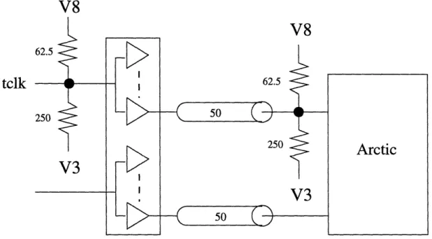
Another consideration for the JTAG signals on the 4x4 routing board is the
reflec-V8
tclk
Figure 3-1: tclk Termination on 4x4 Board
tions due to transmission line effects. The tclk signal would be affected the most by the reflections since it is the clock for the TAP controller on the Arctic chips. Dou-ble clocking can occur because of the reflections. Therefore, the tclk signal should be end terminated to 4V (7V) through a 50 ohm thevenin equivalent resistor with the stripline being 50 ohms. The tclk signal is terminated both into the buffer and into the Arctic chips (Figure 3-1). The considerations for chosing the termination scheme are a 50 ohm stripline, the amount of drive current available, which is -24 ma for driving "high" and 64 ma for driving "low", and meeting the Arctic CMOS logic levels. The stripline was restricted to 50 ohms because in order to change to a higher impedance stripline another layer of the board would be needed. Since the cost of adding another layer to the board would be very costly, especially for just a few signals, the stripline impedance is restricted to 50 ohms. Considering these re-strictions, the tclk termination scheme should produce at least 4V (7V) for a "high" and 0.55V (3.55V) for a "low". Since the Arctic CMOS level requirements are less
than 1.5V (4.5V) for a logic "low" and greater than 3.5V (6.5V) for a logic "high", this termination scheme should work fine. The signals, tms, tdi, and trstb do not need terminations since the trace lengths are short compared to the amount of time the signals have to settle.
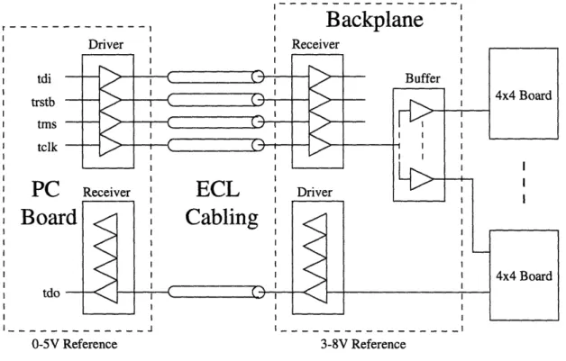
3.2 Voltage Translation
The voltage problem occurs because of the voltage offset of the GTL devices on the 4x4 routing board. As mentioned earlier the GTL devices, including the Arctic chips, are referenced at 3V and 8V. The PC board is referenced at ground and 5V. Since the backplane is referenced at the same voltages as the 4x4 routing board the voltage translation occurs where the PC board connects with the backplane. The drivers and
---
I
Backplane
Driver I | Receiver tdi trstb tms tclkPC
3oar
tdo …-- - -_ - - - - I -0-5V Reference 3-8V ReferenceFigure 3-2: Voltage Translation Diagram
receivers between the PC board and backplane connection, as shown in Figure 3-2, are special ECL drivers and receivers. The drivers convert TTL signals to ECL levels, the
r- -I I I I I I I I I I I I I I I I II I I I I I I I I I I I
-receivers convert ECL signals to TTL signals, and the -receivers have a large common mode range of -1.2V to 7.2V. Because of these special features the drivers can take in the four JTAG output signals from the PC board which are referenced between OV and 5V and convert them to ECL signals, and then the receivers convert the ECL signals into TTL levels which are referenced between 3V and 8V. Since the output of the drivers is between 1.8V and 5V and the receivers' common mode range is between
1.8V and 10.2V (common mode range shifted by 3V), the translation from 0-5V to 3-8V is straight forward. The termination for the ECL signals is a Y termination resistor taken from the built-in Y termination resistor in one of the receiver packages. The reason that an external Y termination resistor is used instead of the internal one is that the ground for an internal termination is actually 3V. Since the driver output is between 1.8V and 5V, the driver might have to sink current. However, the drivers cannot sink current and must drive a minimum amount of current to function properly. For this reason, the termination must be external to the receiver package in order to connect to ground. The signals are converted to CMOS levels through buffers which are already necessary to fan out the signals to all the 4x4 routing boards. The tdi signal only connects to one 4x4 routing board, but the signal still needs to be translated to CMOS levels so the tdi signal passes through a buffer on the backplane,
as well.
Since the tdo signal needs to be sent from the 4x4 routing board to the PC board, a voltage translation in the other direction is required. This voltage translation is a little more complicated. The output of the drivers varies between 4.8V and 8.OV, and the common mode range of the receivers on the PC board is between -1.2V and 7.2V. Since the output of the drivers can be higher than the common mode range of the receivers, the termination scheme has to scale down the voltage that the receivers see. The termination scheme is basically the same as the standard Y resistor in the receiver package, except that the differential receiver inputs are tapping the 60 ohm resistors and the pull down resistor is changed from 90 to 180 ohms (see Figure 3-3). The taps are chosen so that the receivers see one-half of the voltage dropped across the 60 ohm resistors; therefore, the receivers receive voltages in the range of 4.425V
to 6.85V. The pull down resistor is doubled to reduce the current demand on the drivers. The drivers are specified for driving 8ma "low" and 40ma "high". The total current required for the same 90 ohm pull down would be approximately 63ma which exceeds the driver current specificaitons. Since the voltage across the pull down is approximately doubled from 3V to 6V, the pull down resistor is doubled to keep the current through it approximately the same as the normal setup which is within the driver specifications. Unlike the translation of voltage from the PC board to the 4x4 routing boards, the signal going to the PC board can be TTL levels; therefore, a buffer is not used in conjunction with the receivers.
60 60 DO+/RI+
DO-/RI-90g
30 30 30 30 DO+ DO-RI+ 2 RI-180Figure 3-3: PC Board tdo Termination
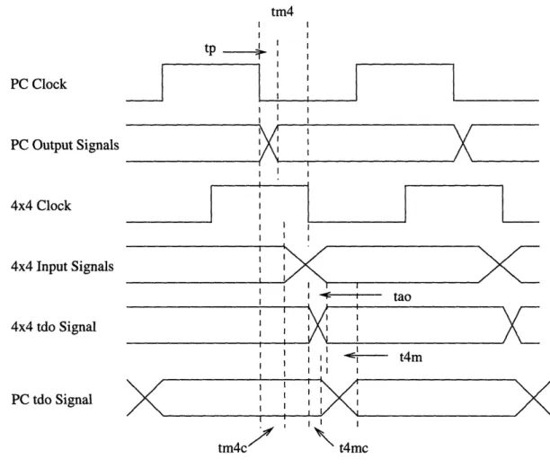
3.3 Timing Requirements
Since the PC board has to clock data out to the 4x4 routing board and also clock in data from the 4x4 routing board using only the clock generated on the PC board, the entire JTAG interface must be considered for doing timing calculations (Figure
3-4). First of all, the tms and tdi signals must arrive in a certain window of time for the tclk signal to clock them into the TAP controller on the Arctic chip. The next important timing consideration is to make sure that the tdo signal coming back from
the 4x4 routing board to the PC board arrives in a certain window of time so that the PC board's clock can capture the signal.
The delays for sending the signals to the Arctic chips on the 4x4 routing boards from
tm4 I I PC Clock PC Output Signals 4x4 Clock I I I I I I II I I I I I I I I I I I III I I 4x4 Input Signals 4x4 tdo Signal PC tdo Signal
I
I I I I __ i,-I Il -I I * i: - tao I I Ii I , <tc: t4m I II
-I___________I _____ I I Itm4c
"
/ Ia I t4mcFigure 3-4: JTAG Signals' Timing
the PC board mainly are: the cabling from the PC to the backplane, the differential
line drivers and receivers for the voltage conversion, the buffers on the backplane, and the buffers on the 4x4 routing board. Because of the standard for JTAG signals,
the signals tms, tdi, and tdo transition on the falling edge of the clock, while the
r i~~~~~~ I 111 # f I II
II
II
II
II
II
I I I I 1* i - tao I : .El I t4m I I I I I I X I I I I I IPC board or TAP controller clocks in the signals on the rising edge of the clock. Therefore, as long as the skew between the data signals and tclk is less than half the period of the clock, there should not be a timing problem in clocking the tms and tdi signals at the Arctic chips. Appendix C.3 shows the calculations for this timing consideration with tclk at 8 MHz, 125 ns.
In considering the other problem of being able to return the tdo signal back in time to be clocked, the total amount of delay from when the PC sends out the tclk signal to when the tdo signal returns to the PC needs to be less than one period of tclk, 125ns. Originally, the total delay needed to be less than half the period; however, the PC board has been modified to capture tdo on the falling edge of tclk so that the total roundtrip delay can be as much as a period of tclk. Besides all the delays mentioned earlier for clocking the signals into the TAP controller on Arctic, the total length of stripline from the backplane to the Arctic chips on the 4x4 routing board and back to the backplane needs to be added, as well as, the differential line drivers' and receivers' delay, and the cabling delay to the PC board. The calculations in Appendix C.3 show that the total amount of delay is less than a period of tclk. One last timing consideration for the tdo signal is to insure that the hold time for the tdo signal is met. The hold time of the FIFO receiving the tdo signal is zero, but the clock that clocks the FIFO is generated through a programmable logic device with a maximum delay of 10ns. With this in mind, the effective hold time is 10ns. The shortest round trip path to the 4x4 routing board passes through two voltage translation drivers and receivers, two lengths of cabling, two lengths of trace, and two buffers. The minimum delay of the drivers, receivers, and buffers alone is 11ns
Chapter 4
Power and Area
4.1 Power
Besides ground, four different voltage levels are required for the 4x4 routing board. Two 5V supplies isolate the GTL from the ECL devices. A 2V supply (ECL 2V) between the 5V supplies shifts the GTL supply 3V higher than the ECL supply (see Figure 2-2). Since the ground for the GTL supply is 3V, it is used for terminating the ECL signals. The terminating voltage for the GTL signals needs to be 4.2V. An additional 1.2V supply referenced off the GTL ground (3V) would be the best choice; however, a reliable 1.2V supply is difficult to construct. For this reason an additional 2V supply across a voltage divider is required to supply the 1.2V termination voltage. This setup has the same advantages of a seperate 1.2V power supply except for a slightly higher power consumption. The advantage of a seperate power supply is that it helps to keep the GTL and ECL terminations seperated. The reason for keeping these terminations seperate is because the noise from the GTL terminations could shift the ECL signals out of the common mode range. However, due to the power constraints on the power supplies, the GTL clock signals for the Arctic chips will be terminated across the ECL 2V supply.
For calculating the power requirement of the power supplies needed, Appendix A, Tables A.3 and A.4 show the power dissipation of all the devices used on the board
be capable of handling 20.01 watts per a board, the GTL 5V supply needs to be capable of handling 26.94 watts per a board, the ECL 2V supply needs to be capable of handling 10.93 watts per a board (including the GTL clock terminations), and the GTL 2V supply needs to be capable of handling 12.13 watts per a board . For a 16 board system, the power supplies should be at least 321 watts and 432 watts for the 5V supplies, and 175 watts and 195 watts for the 2V supplies. Currently, the 16 board system will have two 500 watt 5V supplies and two 200 watt 2V supplies. The only other limitation on the power supplies is that the total power be less than 1200 watts. The total power requirement for the 16 board system is 1123 watts. Even though one of the 2V supplies is almost at its maximum output, since the total power in the system is less than 1200 watts, the power supply company has assured that the 2V power supply will not have a problem with supplying the power, especially since this is the absolute maximum amount of power required on the 2V supply. The average power requirement of this 2V supply will be approximately 75% of the maximum, which is approximately 150 watts.
Concerning the GTL clock terminations mentioned earlier, the total power demand on the GTL 2V supply, including the GTL clock terminations, would be just over 200 watts for the worst case scenario in a sixteen board system. By moving the GTL clock terminations to the ECL 2V supply, which has extra power to spare, the requirement for the GTL 2V supply falls to just under 200 watts for the worst case scenario as shown in the previous paragraph. The reason that the GTL clock signals out of all the other GTL signals were chosen to be moved to the ECL 2V power supply is that the GTL clock signals are differential pairs which means the current is approximately constant and so the GTL clocks do not add much noise across the ECL 2V supply.
4.2
Area
The area of the board is mainly due to the area needed by the chips. The board has four layers and five power planes. The four layers of the board should be sufficent to handle all the routing; therefore, only the area needed to mount the chips and
Chapter 5
Conclusion
In summary, I designed the 4x4 routing board in its entirety. I designed the sections for transmitting and receiving signals to the processors that connect to the 4x4 routing board and to other 4x4 routing boards. I designed the section for transmitting the JTAG signals from the PC board to the 4x4 routing board and back to the PC board, including modifications to the PC board and signal distribution on the backplane. As part of designing these sections, I selected components (Appendix A, Table A.5) and created an inital layout of the board for calculating the power and area requirements for the board (Appendix B, Figure B-3). Finally, with these selected components, I carried out detailed calculations for timings, voltage conversions, transmission line effects, and power requirements (Appendix C). In the following sections, I will cover the remaining concerns with designing the 4x4 routing board and possible testing procedures for when the board is fabricated.
5.1 Other Board Design Issues
For the link technology, there are two constraints for trace lengths in order to insure the GTL to ECL conversion. The trace lengths for the Arctic data signals to the ECL registers should be equal or greater than the sum of the lengths of trace from the Arctic chip through the AMCC PLL, through the delay line chip, and through the clock buffer to the ECL registers. The reason for this restriction on the trace lengths
is because if the trace lengths for the Arctic data to the ECL registers were much shorter than the sum of the traces for generating the ECL clock signal to the ECL registers, then the clock received at the ECL registers could be too late for clocking the Arctic data. The other constraint is that the trace length for the inverted Arctic clock to the ECL flip flop should be equal to or less than the sum of the lengths of
trace from the Arctic chip through the AMCC PLL, through the delay line chip, and through the clock buffer to the ECL flip flop. If the trace between the Arctic chip and the ECL flip flop were much longer than the sum of the trace lengths for generating the ECL clock to the flip flop, then the flip flop may be clocked too early to capture the Arctic clock. Both these restrictions should be clear from Appendix C.1. The receiving side of the 4x4 routing board does not have any strong constraints for the trace lengths since the receiving side can handle a large amount of skew (Appendix
C.2).
Both the AMCC PLL and the Arctic chip require some additional hardware for these chips to function properly. The AMCC PLL requires an external PLL filter and an external power supply filter. Suggested designs are in the data sheet. The Arctic chip requires a 0.8V (3.8V) reference voltage and a 40 MHz clock. A voltage divider network across the GTL voltages (V5 and V3) with a capacitor should be sufficient for the reference voltage. A single 40 MHz crystal oscillator will supply each Arctic chip with the necessary 40 MHz clock by passing through a buffer which has a fanout of five. The 40 MHz clock to each Arctic chip should be terminated at the Arctic chips. These signals should be terminated to 4V (7V) exactly the same as the JTAG clock signals are terminated (Figure 3-1). The only difference between the termination of the JTAG clock signals and the 40 MHz clock signals is that the crystal oscillator connecting to the buffer should not be terminated going into the buffer, but the crystal oscillator needs to be very close to the buffer.
One last consideration for the 4x4 routing board is the placement of the Arctic chips and its heat sink. The Arctic chip which receives the tdi JTAG signal into the board and the Arctic chip which sends the tdo JTAG signal off the board should be close to the GTL connectors. The reason for this is that the Arctic tdo signal drivers are
somewhat weak so the shorter the distance for the tdo signal drivers to drive across the better. In addition, the heat sinks on the Arctic chips need to be setup such that a maximum of two heat sinks are in the same plane of air flow, and the minimum distance between them is one and a half inches. Some termination resistors for the Arctic chips can be placed under the heat sink, but not all of them. A suggested placement of the devices is shown in Appendix B, Figure B-3.
5.2 Possible Testing Procedures
Assuming that the Arctic chips will have been tested, the main testings on the 4x4 routing board should check the JTAG signals and the link technology for getting data to and from Arctic. The testing can be taken care of mostly in software. For testing the JTAG signals, the PC board can be connected to the backplane and into a single 4x4 routing board. The backplane should be available by the time that the 4x4 routing board is fabricated; however, a dummy backplane can be constructed easily to connect the PC board to the 4x4 routing board. The PC board should then be programmed to shoot and capture data to setup the registers in the Arctic chips. After checking out the JTAG signals and programming the registers, packets of information can be sent to the 4x4 routing board with the links looping back to themselves in order to check the link technology. These tests, which another researcher will be working on, should verify most of the functionality of the 4x4 routing board. Additional multi-board tests should be used to verify the links between 4x4 routing boards.
Appendix A
Table A.1: AMCC PLL Phase Selections
PHSEL1 PHSELO Phase Relationship
0 0 All at same phase
0 1 Outputs skewed by 90 degrees from
each other
1 0 FOUT1 leads FOUTO by minimum
phase, FOUT2 lags FOUTO by minimum phase, and FOUT3 lags
FOUTO by 90 degrees
1 1 Outputs skewed by minimum phase
(determined by the divider selection, and the VCO frequency) from each
other.
Table A.2: AMCC PLL Phase Resolution
FOUTO-3 Divider VCO PECL Min Phase
Freq Select Freq Freq Resolution
80 MHz 4 320 MHz 160 MHz 3.125 ns 66 MHz 4 266 MHz 133 MHz 3.75 ns 50 MHz 4 200 MHz 100 MHz 5.0 ns 40 MHz 4 160 IlMHz 80 MHz 6.25 ns 40 MHz 8 320 MHz 160 MHz 3.125 ns 33 MHz 8 266 MHz 133 MHz 3.75 ns 25 MHz 8 200 MHz 100 MHz 5.0 ns 20 MHz 8 160 MHz 80 MHz 6.25 ns
Note: The PECL output is not affected by the phase select inputs.
Table A.3: Device Power
Quantity Max Power (Watts) Device
4 6 Arctic chips
2 0.075 CMOS Clock Buffer
1 0.2 40 MHz crystal oscillator
4 1.125 AMCC PLL
2 0.9203 ECL Delay line
4 0.345 ECL Clock Buffer
4 0.145 ECL flip flop
16 0.51 ECL registers
Table A.4: Termination Power
Quantity Max Power (Watts) Termination Type
224 0.0300 Diff ECL 3V termination
72 0.0448 SE ECL 3V termination
32 0.0305 GTL Clock 4.2V termination
288 0.0419 GTL 4.2V termination
4 0.0095 GTL 0.8V (3.8V) reference
4 0.0048 ECL 3.8V reference
9 0.2874 JTAG 4.OV termination
Table A.5: 4x4 Board Component Listing
Part # Quantity Description
536297-3 4 AMP Connectors (GTL)
102A0-52XXVC 4 3M Connectors (ECL)
??? 4 Arctic chips
MX045-40.000 1 TTL 40.0 MHz Xstal osc.
IDT49FCT805A 2 CMOS buffer/clock driver
S4405 4 AMICC PLL
DECLDL-2-4 2 Dual ECL delay line
SY100Elll 4 ECL clock buffer
SY100E452 16 ECL register chip
SY100EL52 4 ECL flip flop
SY100E116 16 ECL line receiver chip
768201???G?? 8 50 ohm resistor pack
766141???G?? 2 50 ohm resistor pack
766081???G?? 10 50 ohm resistor pack
??? 8 50 ohm resistor
766165???G?? 16 125/86 ohm resistor pack
766085???G?? 16 125/86 ohm resistor pack
??? 9 250 ohm resistor ??? 9 62.5 ohm resistor ??? 4 334 ohm resistor ??? 4 501 ohm resistor ... ??? . 4 168 ohm resistor ??? 4 252 ohm resistor ??? ??? 0.luf capacitor ??? ??? O.Oluf capacitor
Appendix B
Figures
Figure B-2: ECL to GTL Conversion
00
Cj - ' 2 5 ~ ~~~~~ UU h W I >4I
/ \ - / \
0 X11 .zv -7I
---A > N/Y LA ) I
I I C)' I_
bA I, A· A I i---Im
·2rU ... gsl . . . .[]I
ww~~7
- - - - -EZI F2 DFailL
i
I L I N -E-7iD Ml,, . .. . . . .. . . .. P] R U.2 IB
B
--FE U'E,
m
H
[g lE F
9
C[
E m [g
H Iff
[ g [g
10"Figure B-3: 4x4 Board Initial Layout
--- I 19
H-19
19
H-E Hm
E
P-[g El[g m
E Eo
g
FEi ME R.27-7
[]
[]
I . RLII N I .2 F-cc 0 I U U U U: 2 E U -In .2 :F-I0= . . . .2 2 0 U3 E U .j U IAppendix C
Calculations
C.1 ECL Transmission
Table C.1: ECL Transmission Timings
Name Min(ns) Max(ns) Description
tpll 1.5 AMCC PECL clock advance
tv 1.0 AMCC clock advance tolerance
tskew 0.4 AMCC clock skew
tsl 0.15 ECL register setup time
thl 0.2 ECL register hold time
ts2 0.125 ECL flip flop setup time
th2 0.15 ECL flip flop hold time
tslop 0.75 Arctic edge to edge variance
tperiod 12.5 Arctic data transition time
tda 0.2 3.15 Arctic clock to data out
tea 0 0.2 Arctic contamination delay
tbuff 0.43 0.63 Clock buffer delay
1) The X2 clock is early enough for Arctic data?
min(tpll - tv - tskew - tbuf f + tdelay) > max(-tca + thl + tslop)
1.5 - 1 - 0.4 - 0.63 + tdelay > -0.2 + 0.2 + 0.75
tdelay > 1.28
max(tpll + tv + tskew - tbuf f + tdelay) < min(tperiod
- tda - tsl - tslop)
1.5 + 1 + 0.4 - 0.43 + tdelay < 12.5 - 3.15 - 0.15 - 0.75
tdelay < 5.98
3) The X2 clock is early enough for Arctic clock?
min(tperiod - tpll + tv + tskew + tperiod/2 + tdelay - tbuf f) > max(tslop + ts2)
12.5 - (1.5 + 1 + 0.4 + 6.25 + tdelay - 0.43) > 0.75 + 0.125
tdelay < 2.905
4) The X2 clock is late enough for Arctic clock?
max(tperiod
- tpll - tv - tskew + tperiod/2
+ tdelay - tbuf f) <
min(tperiod - tslop - th2)
12.5 - (1.5 - 1 - 0.4 + 6.25 + tdelay - 0.63) < 12.5 - 0.75 - 0.15
tdelay > -4.82
Result: 1.28ns < tdelay < 2.905ns
C.2 ECL Reception
Table C.2: ECL Receiver Timings
Name Min(ns) Max(ns) Description
tperiod 12.5 Arctic data transition time
tas 1.3 Arctic link setup time
tah 0 Arctic link hold time
tcbs 0.2 ECL clock buffer skew
trd 0.475 0.80 ECL register clock to out delay
tfd 0.335 0.62 ECL flip flop clock to out delay
tbd 0.15 0.55 ECL line receiver delay
max(tf d + tbd + tcbs) < min(tperiod/2 - tah)
0.62 + 0.55 + 0.2 < 6.25 - 0 1.19 < 6.25
2) Reg Clock is late enough to clock the data?
max(trd + tbd + tas) < min(tperiod/2 - tcbs + tf d + tbd)
0.80 + 0.55 + 1.3 < 6.25 - 0.2 + 0.335 + 0.152.63 < 6.535
Result: Still able to handle almost 4 ns more of skew.
C.3 JTAG Signals
Table C.3: JTAG Signal Timings
Name Min(ns) Max(ns) Description
tperiod 125 JTAG clock period
tas 20 - Arctic TAP controller setup time
tah 20 - Arctic TAP controller hold time
tpcs 12 - PC board FIFO setup time
tpch 10 - PC board FIFO hold time
tattd 1.5 2.5 AT&T Driver propogational delay
tattds 0.2 0.5 AT&T Driver skew
tattr 2.5 4.0 AT&T Receiver propogational delay
tcb 1.5 5.5 Fast CMOS Buffer/Clock Driver delay
tcbs 1.0 1.2 Fast CMOS Buffer/Clock Driver skew
tp 7.0 26.0 PC Board clock to output delay
tao 10.0? Arctic clock to output delay
C.3.1
Clocking tdi and tms
skew(tm4) + tp + tas < tperiod/2
max(tattds + max(tattr) - min(tattr) + 3(tcbs) + tp + tas) < tperiod/2
0.5 + 4.0 - 2.5 + 3(1.2) + 26 + 20 < 62.551.6 < 62.5
Result: Capable of handling 10.9ns of more skew due to the cabling, trace, etc.
C.3.2
Clocking tdo
Assuming 6ft cabling at 1.5ns/ft and 0.5m of trace at 1.38x10⁸m/s (er = 4.7):
max(tm4 + tao + t4m + tpcs) < tperiod
max(tattd+cabling+tattr+3(tcb)+trace+tao+trace+tattd+cabling+tattr+tpcs)
<
tperiod
2.5 + 6/1.5 + 4.0 + 3(5.5) + 0.5/0.138 + 10 + 0.5/0.138 + 2.5 + 6/1.5 + 4.0 + 12 < 125
66.75 < 125
Result: An extra 58.25ns for longer cabling, trace length, or Arctic clock to output
Bibliography
[1] Andy Boughton, Steve Chamberlin, Tom Durgavich, Wing Chi Leung, Greg
Pa-padopoulos, etc., DRAFT Arctic User's Manual
[2] Rajat Moona, JTAG Controller Board
[3] G. Andrew Boughton, Arctic Routing Chip