HAL Id: hal-02324315
https://hal.archives-ouvertes.fr/hal-02324315
Submitted on 1 Nov 2019HAL is a multi-disciplinary open access archive for the deposit and dissemination of sci-entific research documents, whether they are pub-lished or not. The documents may come from teaching and research institutions in France or abroad, or from public or private research centers.
L’archive ouverte pluridisciplinaire HAL, est destinée au dépôt et à la diffusion de documents scientifiques de niveau recherche, publiés ou non, émanant des établissements d’enseignement et de recherche français ou étrangers, des laboratoires publics ou privés.
Charge injection phenomena at the metal/dielectric
interface investigated by Kelvin probe force microscopy
Florian Mortreuil, Christina Villeneuve-Faure, Laurent Boudou, K
Makasheva, G. Teyssedre
To cite this version:
Florian Mortreuil, Christina Villeneuve-Faure, Laurent Boudou, K Makasheva, G. Teyssedre. Charge injection phenomena at the metal/dielectric interface investigated by Kelvin probe force microscopy. Journal of Physics D: Applied Physics, IOP Publishing, 2017, 50 (17), pp.175302. �10.1088/1361-6463/aa665e�. �hal-02324315�
1 Charge injection phenomena at metal/dielectric interface investigated by Kelvin Probe Force
Microscopy
F. Mortreuil, C. Villeneuve-Faure,* L. Boudou, K. Makasheva, G. Teyssedre
LAPLACE (Laboratoire Plasma et Conversion d’Energie), Université de Toulouse, CNRS, INPT, UPS, Bat 3R3, 118 route de Narbonne, F-31062 Toulouse Cedex 9, France
Abstract
The understanding of charge injection mechanism at metal/dielectric interface is crucial in many applications. A direct probe of such phenomenon requires a charge measurement method whose spatial resolution is compatible with the characteristic scale of phenomena occurring after injection, like charge trapping, and with the geometry of samples under investigation. In this paper, charge injection at metal/dielectric interface and their motion in silicon nitride layer under tunable electric field are probed at nanoscale using a technique derived from Atomic Force Microscopy. This was achieved by realizing embedded lateral electrode structures and using surface potential measurement by Kelvin Probe Force Microscopy (KPFM) to provide voltage, field and charge profiles close to the metal/dielectric interface during and after biasing the electrodes. The influence of electric field enhancement at the interface due to the electrode geometry was accounted for. Electron and hole mobility was estimated from surface potential profiles obtained under polarization. Charge dynamic was investigated during depolarization steps.
Keywords: KPFM, Thin dielectric layer, Lateral electrodes, Charge injection, Metal/dielectric interface
1. Introduction
An important property of insulating materials is their ability to accumulate charges under electrical stress. Even though this effect is useful for some applications, charge injection and accumulation in dielectric layers remain the main cause of failure in many devices. Therefore, knowledge of the space charge amount and its distribution in the dielectric layer is crucial to improve understanding on charge generation and storage mechanisms. Various space charge probing techniques were developed during the past decades, based on charge perturbation by acoustic or thermal excitation [1, 2] (Pulse ElectroAcoustic method, Pressure Induced Pulse Wave Propagation method, Laser Intensity Modulation Method, etc.). However, due to their low spatial resolution, around few micrometers [3, 4], they fail to provide direct charge distribution in thin dielectric layers (thickness less than few microns) [5, 6]. Electrical modes like Electrostatic Force Microscopy (EFM) [7, 8] and Kelvin Probe
2 Force Microscopy (KPFM) [9, 10] were derived from Atomic Force Microscopy to overcome this drawback. These methods were extensively used to study thin dielectric films and manage to reach atomic resolution for KPFM in non-contact mode under vacuum [11, 12]. Focusing on charge retention in thin dielectrics, these techniques provide results about carriers dynamic at nanoscale [5, 13-15] but up to now they fail to measure space charge distribution in three dimensions [13],with notable lack of information about the in-depth charge distribution.
A way to probe charge injection phenomena at the metal/dielectric interface is to use buried lateral electrodes. Under this configuration, the in-depth issue becomes a lateral one. Buried electrodes were already used to investigate charge transport in organic semiconductor using EFM [16, 17] or KPFM [18], mainly combining with current measurements [17, 18]. The obtained results on organic semiconductors, although promising, show strong dependence on the film morphology or on the step at the electrodes [16], which makes the interpretation tricky. Combining buried lateral electrodes to inject charges in thin dielectric layers and KPFM for resulting surface potential measurements, is a quite new and challenging approach. Indeed, to obtain space charge distribution close to the interfaces with resolution of the order of tens of nanometers, and to follow their dynamical behavior with and without applied electric field, surface and interfaces control are crucial. To improve the lateral resolution, a flat surface (small roughness and no step) and a small lift height are needed.
In this contribution, we report on the development of lateral electrode structures to probe charge injection phenomena at metal/dielectric interface and charge motion in dielectric layers by using KPFM measurements. Knowledge of space charge distribution at local scale is necessary to understand mechanisms occurring at the metal/dielectric interfaces which were up to now investigated only by using microscale techniques [20, 21]. The obtained results should have strong impact on the interface characterization and modelling. The first part is dedicated to the description of experimental conditions for sample processing and KPFM measurements. The following part presents procedure to compute the electric field distribution in the dielectric layer and the used methodology to extract electric charge density from surface potential measurements. The last part is dedicated to the results and discussion in terms of charges density profile and charges mobility estimation.
2. Experiments
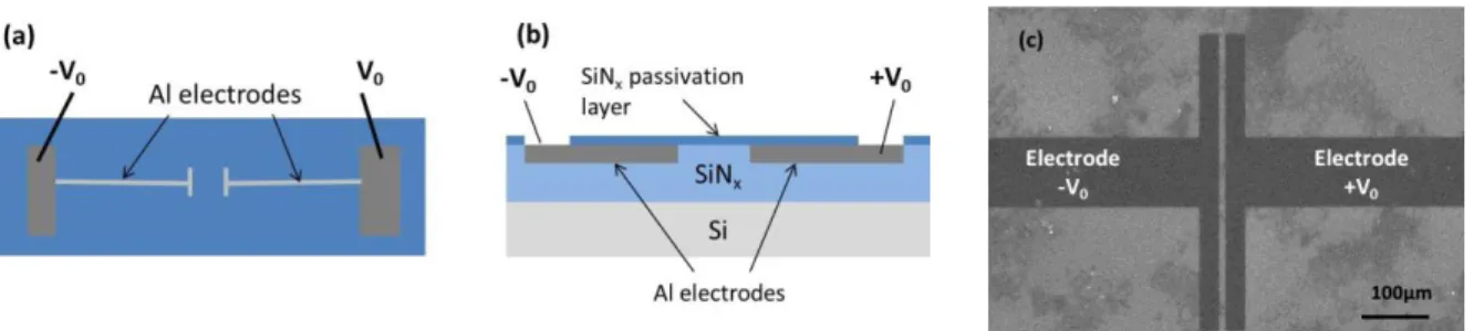
The samples are composed of buried lateral electrodes with different inter-electrode distances (from 5µm to 40µm) as represented in top- and cross-view on figures 1.a. and 1.b., respectively. The investigated dielectric layers are of silicon nitride (SiNx), processed by Plasma Enhanced Chemical
Vapor Deposition [22]. 300nm-thick SiNx layers were deposited on low resistivity silicon wafers.
Aluminum electrodes were buried by lift-off process. A 2.5µm-thick N-LOF photoresist was deposited on the SiNx layer surface and patterned by photolithography. Then, the SiNx was chemically etched to
3 contact and small surface roughness. Contact quality was controlled through observations of the cross-section of the resulting structure by using Scanning Electron Microscopy (SEM). Finally, a 5nm SiNx
passivation-layer was deposited to cover the embedded electrodes in order to prevent from discharge issues between electrodes and AFM tip. The resulting surface is flat enough (less than 5nm-step between the electrode and the dielectric layer) to avoid topography artefacts on the KPFM measurement. Figure 1.c. represents a top-view of the final structure as observed by SEM.
Figure 1. Sample schematic structure in (a) top- and (b) cross-view. (c) SEM top-view image of buried lateral electrodes separated by a distance of 10µm.
KPFM surface potential was measured in Amplitude Modulation mode with a Bruker Multimode 8 set-up using Pt-coated silicon tip in lift mode. We used the common dual-pass mode as scanning method for KPFM measurements [23]. As the sample surface roughness is small (less than 5nm) a small lift of only 10nm was used to minimize parasitic capacitance effect and improve lateral resolution. The cantilever was maintained parallel to the electrode to minimize its contribution. All measurements were performed under dry N2 atmosphere after sample conditioning for 4 min at 120°C
to remove the water layer adsorbed on the surface (in this case the adhesion force is measured close to zero). The electric field was induced by applying bias voltage between the electrodes. This bias can be symmetric ±V0 (i.e. potential difference V = 2V0) or asymmetric V0 with respect to the ground.
Surface potential measurements were performed just after polarization and during the depolarization phase.
3. Computing the electric field distribution and the charge profiles 3.1. Electric field distribution
To provide an accurate estimate of the electrical stress in the structure during charging, a Finite Element Model (FEM) was developed in two dimensions using COMSOL Multiphysics [24]. The resulting model represents the sample structure described above (figure 1.b.), surrounded by an air box of dimensions large enough to avoid edge effects. The relative dielectric permittivity of the silicon nitride layer was taken r = 7.5 which applies for 1 kHz and 23°C. The dielectric layer was supposed
initially free from charges. The silicon substrate backside was set to ground as in the experiment. The Poisson's equation was solved in air and in the dielectric layer to determine the electric field
4 distribution. Meshing was adapted to the layer dimensions. It was refined in the two dielectric layers (studied layer and the passivating one) and at the metal/dielectric and air/dielectric interfaces.
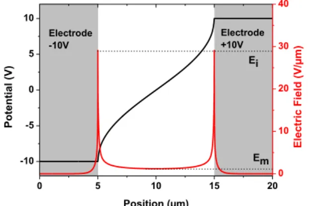
Figure 2 represents the potential and electric field distributions, on the dielectric surface for an inter-electrode distance of 10µm and a symmetric V bias of 20V. Contrary to a plane-plane configuration, the potential varies non-linearly between the electrodes due to their small thickness (70nm) compared to their lateral dimension (few hundreds of µm). This implies a strong electric field enhancement close to the metal/dielectric interfaces. The influence of this field enhancement on charge injection mechanism is further investigated. To provide quantitative figures, two important values of the electric field are defined, as shown on figure 2: (1) Em is the electric field far from electrodes, i.e. in the middle
of the dielectric and (2) Ei is the electric field in the region of enhancement, i.e. close to the electrodes.
0 5 10 15 20 -10 -5 0 5 10 Position (µm) P o te n tial ( V ) 0 10 20 30 40 Em Electrode -10V E lec tr ic F ield ( V /µ m ) Electrode +10V Ei
Figure 2. Potential and electric field profiles at applied symmetric V = 20V between two electrodes separated by 10µm.
3.2. Charge density profile
The simplest hypothesis for determining the charge density profile from the measured KPFM profile consists in assuming that the scanned potential actually corresponds to the inter-electrode potential distribution. To a first approximation, this appears as reasonable hypothesis given the fact that the lift distance and the tip apex are small in respect to the inter-electrode distance. More sophisticated FEM modelling has confirmed the validity of the approximation [25]. From the surface potential VS(x)
measured by AM-KPFM, charge density ρ(x) has been extracted resolving the Poisson's equation:
0 2 2 S r d V x dx ,
(1)
where ε0 is the vacuum permittivity, εr is the SiNx relative permittivity (εr=7.5) and x is the lateral
position. Contrary to K. Faliya et al. [26] no smoothing treatment was applied. The derivation step dx was fixed to 160nm whereas KPFM measurement step was 39nm (512 points over 20µm) to minimize noise effect on derivation process.
5 4. Results and discussion
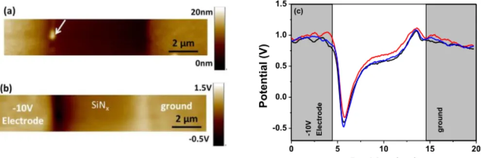
Figure 3.a represents SiNx surface topography with 3nm roughness and less than 5nm-step between
dielectric and electrode. Maintaining such small step between dielectric and passivated-electrode is crucial to avoid crosstalk between topography and surface potential map [27, 28]. Before polarization, the surface potential is flat with no contrast between dielectric and passivated electrodes, and taken as reference potential. Consequently, no correlation is observed between topography and potential map owing to the small topography variation of the surface. This aspect is crucial to guarantee accurate measurements at the metal/dielectric interface. Figure 3.b represents the surface potential map measured, at the same time as topography (figure 3.a), after applying -10V on one of the electrodes for 1 hour, the inter-electrode distance being 10µm. The surface potential of the dielectric layer (figure 3.b) is modified by the amount of charges which were injected and stored. According to Sadewasser et
al. [27], as the surface potential modification appears far from the step (at 2µm in figure 3.c.), its
shape should not be modified by the step height. Moreover, note that the observed surface topography heterogeneities (arrow on figure 3.a.) are not correlated with the potential patterns (figure 3.b). On figures 3.a and 3.b the dielectric/metal interface appears smooth. Potential profiles which were extracted from the potential map (figure 3.b.) along three different lines are plotted in figure 3.c. One finds two peaks, a positive one close to anode and a negative one close to cathode, ascribed to the injection of holes and electrons, respectively. Comparing the potential profiles depicted in figure 3.c. a variation of 16% of potential maximum and Full-Width at Half Maximum (FWHM) of the peak is observed. 0 5 10 15 20 -0.5 0.0 0.5 1.0 1.5 grou nd Potenti al (V) Position (µm) (c) -10 V E lec trode
Figure 3. (a) Topography and (b) Surface potential measured simultaneously by AM-KPFM in lift mode after −10𝑉/0𝑉 applied for 1h on electrodes separated by 10µm. (c) Surface potential profiles along different lines of the potential map.
4.1. Injection
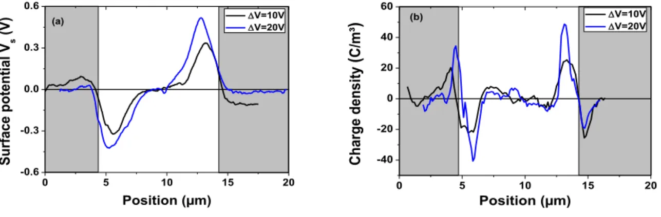
Figure 4.a. represents surface potential profiles measured for different symmetric bias applied to electrodes separated by 10µm. Surface potential was acquired after bias removal. When the applied potential is increased, the surface potential is modified mainly in amplitude and in some cases in position. The charge density profile was estimated from the surface potential measurements for each
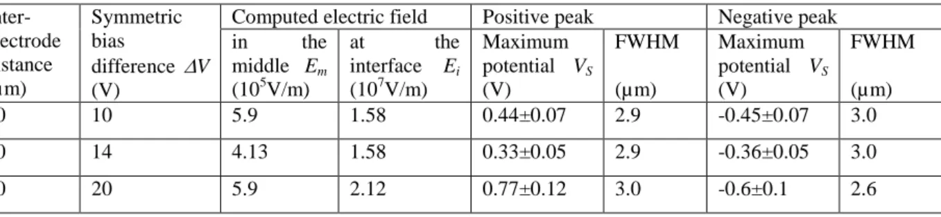
6 polarization configuration after using equation (1). Charge profiles, depicted on figure 4.b., emphasize that negative charges are trapped close to the cathode and positive charges are trapped close to the anode. Moreover, related image charges are revealed over each electrode. These profiles provide interesting information: (i) charges remain close to the electrodes (distance less than 2µm from the electrode) even for long injection time and (ii) no significant amount of charges is measured in the middle of the inter-electrode space. This should be related to the electric field enhancement close to interfaces, whereas the electric field in the middle of the inter-electrode space remains constant and low (cf. figure 2). The motion of charges is an important process to analyze. However, due to the noise produced by the two-steps derivation of the potential, it is quite difficult to estimate changes in time of the peak maximum. Besides, more work is needed to develop an accurate space charge profile computing method. As potential and density profiles are related by the Poisson's equation, and in order to limit noise effects, we use the change in position of the potential peaks to estimate the charge cloud motion, hence the charges mobility. Such reasoning is supported by the fact that the measured potential is relatively flat in the middle of the inter-electrode space, meaning that the field there is small. Under these conditions, the two trapped charge clouds can be considered as independent; the mutual influence appears to be small. As highlighted on figure 2, the electric field enhancement occurs close to the interfaces because of the electrodes geometry. By changing the applied bias and/or the inter-electrode distance, it is possible to act in different ways on the mean electric field between the electrodes (driving the charge transport) and on the field at the electrodes (controlling the charge injection). Results on the field values and voltage peak are summarized in Table 1.
0 5 10 15 20 -0.6 -0.3 0.0 0.3 0.6 Surfac e potent ial V s (V) Position (µm) V=10V V=20V (a) 0 5 10 15 20 -40 -20 0 20 40 60 Cha rge density ( C/m ³ ) Position (µm) V=10V V=20V (b)
Figure 4. Influence of 180min-polarization bias on (a) surface potential profile measured by KPFM and (b) resulting charges profile. Cathode to the left; anode to the right during polarization.
Comparison of the 1st and the 3rd rows in Table 1 shows that by acting on the inter-electrodes distance the field at the electrode (injecting field Ei) can be modulated keeping the same field in the middle of
the sample. From the resulting potential profiles, it can be deduced that the magnitude of both peaks (negative and positive) increases substantially when the interface field is increased. Higher amount of
7 charges is obtained for 20µm inter-electrode distance (maximum at 40C/m3) compared to 10µm inter-electrode distance (maximum at 25C/m3). This feature confirms that the potential builds up due to charges generated by injection at both electrodes.
Table 1. Influence of the electric field in the middle of the sample and field enhancement at the interfaces on the maximum potential and the FWHM of both peaks. Error bars are calculated considering 16% variation. Inter-electrode distance (µm) Symmetric bias difference V (V)
Computed electric field Positive peak Negative peak
in the middle Em (105V/m) at the interface Ei (107V/m) Maximum potential VS (V) FWHM (µm) Maximum potential VS (V) FWHM (µm) 10 10 5.9 1.58 0.44±0.07 2.9 -0.45±0.07 3.0 20 14 4.13 1.58 0.33±0.05 2.9 -0.36±0.05 3.0 20 20 5.9 2.12 0.77±0.12 3.0 -0.6±0.1 2.6
The position of maximum potential was estimated for each peak at the beginning ( 30s) and at the end (180min) of the polarization step. The velocity of the charge cloud was calculated from the shift in position of the potential peak: 4nm/min for holes and 6nm/min for electrons with an uncertainty of 7% on the shift estimation which leads to an incertitude of 0.4nm/min for electrons velocity and 0.3nm/min for holes velocity. Using the so-obtained velocity and the mean electric field (i.e. electric field far from interfaces) the determined value of the mobility of electrons is ≈ 1.2×10⁻¹¹ cm2V-1s-1 and the one for holes is
0.8
×10-11 cm2V-1s-1. The obtained value for mobility of electrons is of the same order of magnitude as the one reported for organic dielectric materials like polyethylene [29]. It is much smaller compared to the value deduced for thermal SiO2 (≈ 10-9
cm2V-1s-1) [30] using EFM data on similar structures as those presented in this work. Estimates of mobility in insulations can differ for many reasons: (i) structural characteristics and chemical composition (SiO2 vs SiNx), and the related
elaboration process; (ii) procedure used to inject charges: in Ref. 30 the charges were injected or deposited on the dielectric surface under higher fields using an AFM tip, compared to the present study with buried planar electrodes; (iii) conduction mechanism involved: if charges are deposited on the surface, their drift can be provided through surface states. Their apparent mobility is then higher than the one in the material bulk. Also, depending on whether the charges are thermalized or not during measurements, their mobility can be considerably different. For example Mott et al. [31] estimated the band mobility for electrons in SiO2 to 20 cm
2
V-1s-1, which is ten orders of magnitude larger than the associated one to hopping between trap sites by Lambert et al. [30]; (iv) dependence of carrier mobility on the driving electric field.
Considering the results in Table 1 and charge profiles (figure 4.b.), the maximum potential or charge density is the same for both peaks, meaning that electrons and holes have nearly the same injection
8 rate. The energy diagram for an Al/SiNx interface predicts energy barrier of around 2.1eV for electrons
and 2.9eV for holes [32]. Therefore, electrons should be injected more easily than holes.
Moreover, charges of both signs are detected after application of an interface field of only 10kV/mm (obtained for V of 5V with an inter-electrode distance of 5µm). The barrier to injection is decreased by only 0.1eV with such field and is still too high to be overcome at room temperature. Consequently, charges would be injected in interface traps with energy levels in the band gap: the relatively low estimated mobility is consistent with transport through trap states.
4.2. Decay
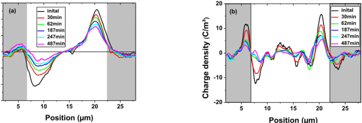
After 180min polarization step, the voltage profile was monitored for several hours with the electrodes being at floating potential. The evolution of the potential profile is reported on figure 5.a. Decrease of the maximum potential, slight peak broadening, and peak shift towards the dielectric bulk are observed for a short time (less than 30min). The amplitude of the negative peak decreases following an exponential-like law. About 30% of the measured initial potential value remains even after 8h of discharge. For the positive peak, the voltage drop is much slower, by only 30% after 8h. This dynamical behavior is comparable to the one obtained for microscale contact charging in SiNx
dielectrics in case of dissipation in the volume [21, 33]. As previously, the charge density profile was extracted from surface potential measurement using equation (1) and depicted on figure 5.b. As for the potential profile, the charge density evolution with time after polarization emphasizes that the charge distribution broadens, moves slightly away from the electrode and substantially decreases in amplitude.
The charge displacement velocity was estimated to around 1nm/min for electrons and holes from the change in position of positive and negative peaks. This velocity is smaller than the one measured during the polarization step owing to the fact that charges move under the effect of their own electric field which is smaller than the one applied during charging.
5 10 15 20 25 -0.6 -0.4 -0.2 0.0 0.2 0.4 0.6 inital 30min 62min 187min 247min 487min Potenti al (V) Position (µm) (a) 5 10 15 20 25 -20 -10 0 10 20 inital 30min 62min 187min 247min 487min Position (µm) Char ge densi ty ( C/m³ ) (b)
Figure 5. Evolution of (a) potential profile and (b) related charge density profile with time after polarization step (180min at V =20V) on lateral electrodes separated by 15µm.
9 5. Conclusion
The proposed method for characterization of charging phenomena of insulators by using embedded electrodes offers several advantages over surface charge deposition using AFM tip in the sense that the field near the electrode is better controlled, less divergent, and with the absence of triple point (air-metal-dielectric). Injection processes and transport in the bulk can be directly probed without the problem of surface dissipation of the charge and possible impact of surrounding atmosphere. Estimations of charges mobility were obtained considering shift in the potential curve. Critical points for further development of the method are the robustness of the model used to extract charge profiles and the spatial resolution: as such, potential curves integrate the response; proper modelling and derivation are necessary to reach ultimate charge localization and to estimate accurately charge density profile identifying artefacts. Such approaches are currently under way.
Acknowledgement
This work was partly supported by the French RENATECH network.
References
[1] Fleming RJ 2005 Space charge profile measurement techniques: recent advances and future directions IEEE Trans. Dielectr. Electr. Insul. 12 967.
[2] Imburgia A, Miceli R, Riva Sanseverino E, Romano P and Viola F. 2016 Review of space charge measurement systems: Acoustic, thermal and optical methods IEEE Trans. Dielectr. Electr. Insul. 23 3126.
[3] Maeno T and Fukunaga K 1996 High-resolution PEA charge distribution measurement system
IEEE Trans. Dielec. Electr. Insul. 3 754.
[4] Petre A, Marty-Dessus D, Berquez L and Franceschi JL 2004 Three-dimensional space charge cartographies by FLIMM in electron irradiated polymers J. Appl. Phys. 43 2572.
[5] Stevens GC and Baird PJ 2005 Nano- and Meso-measurement methods in the study of dielectrics
IEEE Trans. Dielectr. Electr. Insul. 12 979.
[6] Boyer L, Fruchier O, Notingher P, Agnel S, Rousset B and Sanchez JL 2010 Analysis of data obtained using the thermal-step method on a MOS structure - An electrostatic approach IEEE Trans.
Ind. Appl. 46 1144.
[7] Ishii M 2010 Static states and dynamic behaviour of charges : observation and control by scanning probe microscopy J. Phys.: Condens. Matter. 22 173001.
10 [8] Terris B, Stern J, Rugar D and Manin H 1989 Contact electrification using force microscopy Phys.
Rev. Lett. 63 2669.
[9] Sadewasser S and Glatzel T 2012 Kelvin Probe Force Microscopy: Measuring and Compensating Electrostatic Forces' S. eds. Springer Series in Surface Sciences 48.
[10] Jacobs HO, Leuchtmann P, Homan OJ and Stemmer A 1998 Resolution and contrast in Kelvin probe force microscopy J. Appl. Phys. 84 1168.
[11] Bieletzki M, Hynninen T, Soini T, Pivetta M, Henry C, Foster A, Esch F, Barth C, and Heiz U 2010 Topography and work function measurements of thin MgO(001) films on Ag(001) by nc-AFM and KPFM Phys. Chem. Chem. Phys. 12 3203.
[12] Barth C. and Henry C.R. 2006 Kelvin probe force microscopy on surfaces of UHV cleaved ionic crystals Nanotechn. 17, 5155.
[13] Borowik L, Koku K, Theron D and Melin T 2010 Calculating Kelvin force microscopy signals from static force field Appl. Phys. Lett. 96 103119.
[14] Rezende C A, Gouveia R F, da Silva M A and Galembeck F 2009 Detection of charge distributions in insulator surfaces J. Phys.: Condens. Matter 21 263002.
[15] Saint Jean M, Hudlet S, Guthmann C, and Berger J 1997 Charge dynamics and time evolution of contact potential studied by atomic force microscopy Phys. Rev. B 56 15391.
[16] Jaquith M., Muller E. M. and Marohn J. A. 2007 Time-resolved Electrostatic Force Microscopy of Charge Trapping in Polycrystalline Pentacene J. Phys. Chem. B 111, 7711.
[17] Ng T. N., Silveira W. R. and Marohn J. A. 2007 Dependence of charge injection on temperature, electric field and energetic disorder in an organic semiconductor” Phys. Rev. Lett. 98, 066101.
[18] Taylor D. M., Morris D. and Cambridge J. A. 2004 Time evolution of the electric field at electrode interfaces with conducting polymers Appl. Phys. Lett. 85, 5266.
[19] Silveira W. R. and Marohn A. 2004 Microscopic view of charge injection in an organic semiconductor Phys. Rev. Lett. 93, 116104.
[20] Lewis T.J. 1994 Nanometric Dielectrics IEEE Trans. Dielectr. Electr. Insul. 1, 812.
[21] Mizutani T., Takai Y., Osawa T. and Ieda M. 1976 Barrier heigths and surface states of metal-polymer (PET) contacts J. Phys. D: Appl. Phys. 9, 2253.
11 [22] Zaghloul U., Papaioannou G. J., Coccetti F., Pons P. and Plana R. 2010 A systematic reliability investigation of the dielectric charging process in electrostatically actuated MEMS based on Kelvin probe force microscopy J. Micromech. Microeng. 20, 064016.
[23] Albrecht TR, Grutter P, Horne D and Rugar D 1991 Frequency modulation detection using high-Q cantilevers for enhanced force microscope sensitivity J. Appl. Phys. 69 668.
[24] COMSOL Multiphysics 5.1.1.145 (2014)
[25] Emmerich F. and Thielemann C. 2016 Real-space measurement of potential distribution in PECVD ONO electrets by KPFM Nanotechnology 27, 205703
[26] Faliya K., Kliem H. and Dias C. J. 2016 Investigations of Space Charge Distributions by Atomic Force Microscope Proc. IEEE International Conference on Dielectrics (Montpellier, France) 219.
[27] Sadewasser S., Leendertz C., Streicher F. and Lux-Steiner M. Ch. 2009 The influence of surface topography on Kelvin Probe Force Microscopy Nanotechnology 20, 505503.
[28] Bardet S., Popoff M., Diesinger H., Deresmes D., Theron D. and Melin T. 2014 Cross-talk artefacts in Kelvin probe force microscopy imaging: a comprehensive study J. Appl. Phys. 115, 144313.
[29] Perlman M. M., Sonnonstine T. J. and St-Pierre J. A. 1976 Drift mobility determinations using surface potential decay in insulators J. Appl. Phys. 47, 5016.
[30] Lambert J., de Loubens G., Guthmann C. and Saint-Jean M. 2005 Dispersive charge transport along the surface of an insulating layer observed by electrostatic force microscopy Phys. Rev. B 71, 155418.
[31] Mott N. F. 1987 Conduction in Non-Crystalline Materials, Clarendon, Oxford.
[32] Brytov I. A., Gritsenko V. A. and Romashchenko Y. 1985 Short-range order and electron structure of amorphous SiNO Sov. Phys. JETP 62, 321.
[33] Villeneuve-Faure C., Makasheva K., Bonafos C., Despax B., Boudou L., Pons P. and Teyssedre G. 2013 Kelvin force microscopy characterization of charging effect in thin a-SiOxNy:H layers
deposited in pulsed plasma enhanced chemical vapor deposition process by tuning the Silicon-environment J. Appl. Phys. 113, 204102.