HAL Id: tel-01924456
https://tel.archives-ouvertes.fr/tel-01924456
Submitted on 16 Nov 2018
HAL is a multi-disciplinary open access archive for the deposit and dissemination of sci-entific research documents, whether they are pub-lished or not. The documents may come from teaching and research institutions in France or abroad, or from public or private research centers.
L’archive ouverte pluridisciplinaire HAL, est destinée au dépôt et à la diffusion de documents scientifiques de niveau recherche, publiés ou non, émanant des établissements d’enseignement et de recherche français ou étrangers, des laboratoires publics ou privés.
CoFeB nanowires
Xueying Zhang
To cite this version:
Xueying Zhang. Spin-polarized current-induced domain wall motion in CoFeB nanowires. Micro and nanotechnologies/Microelectronics. Université Paris Saclay (COmUE), 2018. English. �NNT : 2018SACLS104�. �tel-01924456�
domaines magnétiques dans le fil
de CoFeB induit par le courant
polarisé
Spin-polarized current-induced domain
wall motion in CoFeB nanowires
Thèse de doctorat de l'Université Paris-Saclay préparée à Université Paris-Sud
École doctorale n°575 : electrical, optical, bio - physics and engineering (EOBE)
Spécialité de doctorat: Physique
Thèse présentée et soutenue à Orsay, le 15 Mai 2018, par
Xueying Zhang
Composition du Jury :Vincent Jeudy
Professeur, Université Paris-Saclay Président
Catherine Gourdon
Directeur de recherche, Université Pierre et Marie Curie-Paris 6 Rapporteur
Vincent Repain
Professeur, Université Paris Diderot – Paris 7 Rapporteur
Stefania Pizzini
Directeur de recherche, Institut Néel Examinateur
Salim Mourad Chérif
Professeur, Université Paris 13 Examinateur
Nicolas Vernier
Maître de Conférence, HDR , Université Paris-Saclay Directeur de thèse
Weisheng Zhao
Professeur, Université de Beihang Co-Directeur de thèse
Université Paris-Saclay
Espace Technologique / Immeuble Discovery
I
Je souhaite commencer ce manuscrit par adresser mes remerciements sincères aux personnes qui m’ont beaucoup aidé depuis quatre ans et qui ont contribué à l’achèvement de ce mémoire. Cette thèse a été menée dans le cadre de la coopération entre le centre de nanoscience et nanotechnologie (C2N) de l’Université Paris-Saclay et le Fert Beijing Institute de l’Université de Beihang.
Je voudrais tout d’abord adresser mes remerciements à mes directeurs de thèse Monsieur Nicolas Vernier, Professeur à l’Université Paris-Saclay et Monsieur Weisheng Zhao, Professeur à l’Universié de Beihang, qui m’ont accueilli dans leur équipe et qui m’ont soutenu tout au long des quatre ans de travail. J’ai commencé des recherche sur le magnétisme en 2014 sous la direction de M. Weisheng Zhao, qui m’a aidé à former des connaissance foundamentales sur le magnétisme, la spintronique et des méthode de recherche via simulations micromagnétique. En 2015, je commence des recherches expérimentales sur des parois du domaine magnétique sous la direction de M. Nicolas Vernier, qui a développé une microscope de Kerr très puissant et qui m’a appris des techniques de microscopie de Kerr, des technologies pour appliquer du champ magnétique et faire simultanément des tests électriques, des méthodes de recherche expérimentales sur la paroi du domaine. Tous les résultats dans cette thèse ont été obtenus sous la direction patiente de mes deux encadrants. Je tiens à les remercier également de m’avoir aidé à exploiter des démarches de recherche scientifique et à résoudre des problèmes scientifiques ou administratifs.
Je voudrais aussi adresser mes remerciements à Monsieur Dafiné Ravelosona, professeur à l’Université Paris-Saclay, qui m’a accueilli et qui m’a donné beaucoup de conseils précieux pendant la recherche de la thèse.
Je voudrais ensuite remercier les membres de mon jury de leur temps consacré à ma thèse. Je remercie particulièrement, mes rapporteurs professeurs Catherine Gourdon et professeur Vincent Repain pour le regard critique et leurs remarques constructives sur mon travail. Je remercie également Professeur Vincent Jeudy, professeur Stefania Pizzini, et professeur Mourad Cherif qui ont gentiment accepté d’examiner mes travaux de thèse.
J’aimerais aussi adresser mes remerciements à Monsieur Laurent Vila, qui a aidé à concevoir et fabriquer des nanostructures testées dans ce recherche, Monsieur Vincent Jeudy, qui m’a appris des connaissance sur le mouvement de paroi dans le régime transition de dépiégeage et qui m’a aidé à analyser des results expérimentals, Monsieur Bonan Yan, qui m’a appris à utiliser le logiciel Mumax3, Monsieur Yue Zhang, avec qui nous avons conçu la mémoire de racetrack de forme annulaire, Monsieur Qunwen
II
Leng, qui m’a donné des conseils sur le design de la capteur à base de l’élasticité de paroi du domaine, Monsieur Yu Zhang, pour les discussions sur des techniques de nano-fabrication et notre coopération sur la recherche du renversement magnétique des nanodots.
Un grand merci à l'atelier du C2N. Grâce à leur travail scrupuleux et efficace, la fabrication et la mis en place des appareil expérimentaux ont été possibles. Aussi, Je tiens à remercier tous mes collègues de C2N et de l’Université de Beihang, de leur gentillesse et de leur accompagnement. Leurs conseils voire les causeries menés pendant les déjeuners ou les pauses, qui ont beaucoup enrichi mes connaissances profesionnelles ainsi que ma vie quotidienne. Cela a été un grand plaisir de travailler avec eux.
Naturellement, je voudrais aussi remercier tous mes amis chinois et français: Ping Che, Sylvain Eimer, Gefei Wang, Qi An, Jiaqi Zhou, You Wang, Boyu Zhang, Chenghao Wang, Zhiqiang Cao... pour leur accompagnement durant les quatre ans.
Un grand merci à China Scholarship Council (CSC) pour son support de financement pendent ma recherche en France.
Enfin, je souhaite exprimer profonde gratitude à ma famille, dont notamment, mes parents, M. Cheng Zhang et Mme Shuchun Wang, qui m’ont accompagné et soutenu sans condition depuis toujours.
III
Symbols
α: Damping constant γ: Gyromagnetic ratio γDW: DW surface energy
θSH: Spin Hall angle
μ: Exponent constant of the creep law
μ0: Permeability of vacuum
μB: Bohr magneton
𝛍
⃗⃗ 𝑚: Magnetic moment ξ: Non adiabatic constant ρ: Resistivity
σ: Conductivity
𝜎 𝑆𝐻: Polarizing direction of
the spin Hall current τ: Spin torque χ: DW tilting angle φ: Azimuthal angle of magnetization θ: Zenith angle of magnetization 𝜙′: Kerr rotation 𝜙′′: Kerr ellipticity
ћ: Reduced Planck constant Aex: Exchange stiffness
constant
B: Magnetic flux density Bext: Externally applied field
D: DMI constant e: Electric charge Eex: Exchange energy
Ek: Anisotropy energy
Ed: Demagnetizing energy
EZeem: Zeeman energy
EDM: DMI energy
Fpin: Pinning force
g: Landau factor H: Magnetic field
HDM: Effective DMI field
Hdemag: Demagnetizing field
Hext: Externally applied field
Hp_intr: Intrinsic pinning field
HK: Anisotropy field
Hdep: Depinning field
I: Electric current j: Current density
jHM: Current density in heavy
metal layer
jSH: Spin Hall current density
jSTT: Current density for spin
transfer torque
KU: Uniaxial anisotropy
Keff: Effective anisotropy
field kB: Boltzmann constant l: Length 𝑚⃗⃗ : Reduced magnetization vector 𝑚⃗⃗ 𝐷𝑊: Magnetic direction in the center of DW 𝑀⃗⃗ : Magnetization MS: Saturation magnetization P: Polarization ratio Pγ: Laplace pressure associated to DW surface energy
Rcoil: Resistance of coil
t: Time tM: Thickness of ferromagnetic layer T: Temperature TC: Curie temperature v: DW motion velocity w: width
IV
Acronyms
AD-STT: Adiabatic Spin Transfer Torque BLS: Brillouin Light Scattering
BW: Block Wall
DMI: Dzyaloshinskii-Moriya Interaction DW: Domain Wall
FM: FerroMagnetic
FMR: FerroMagnetic Resonance GMR: Giant MagnetoResistance HM: Heavy Metal
MTJ: Magnetic Tunnel Junction
NA-STT: Non-Adiabatic Spin Transfer Torque NW: Néel Wall
PMA: Perpendicular Magnetic Anisotropy RM: Racetrack Memory
SAF: Synthetic AntiFerromagnetic SH: Spin Hall
SHE: Spin Hall Effect SOC: Spin-Orbit Coupling SOI: Spin-Orbit Interaction SOT: Spin-Orbit Torque
SQUID: Superconducting Quantum Interference Device STT: Spin Transfer Torque
TMR: Tunneling MagnetoResistance VSM: Vibrating Sample Magnetometer 1D model: One Dimension model
V
Contents
Abstract ... 1 Résumé ... 3 Chapter 1 Introduction ... 5 Motivation ... 5Organization of the thesis ... 6
Chapter 2 State of the art ... 7
Basics... 7
Magnetic domain walls ... 10
DW profile ... 10
DW surface energy ... 11
DW dynamics ... 13
Field-driven DW motions ... 13
Spin transfer torque driven DW motion ... 19
Spin orbit torque driven DW motion ... 22
Micromagnetic simulations ... 25
Applications of DW in storage, logic, communications and sensor ... 25
DW based sensors ... 26
Racetrack Memory ... 27
Chapter 3 Experimental methods ... 29
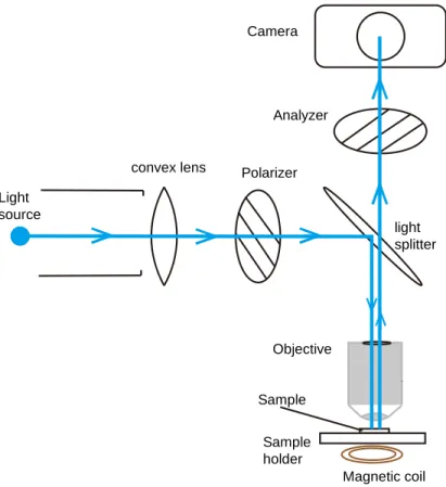
Magneto-Optical Kerr effect ... 29
Typical optical circuits of Kerr microscopes ... 32
Configurations of the Kerr microscope for these studies ... 35
Configurations of magnetic coils ... 36
VI
Power supply for the coil... 43
Configurations for electrical tests ... 47
Samples and the measurements procedures ... 49
Samples ... 49
Nucleation of DW ... 50
Measurement of the DW velocity ... 50
Chapter 4 Surface energy of domain walls ... 52
Direct observation of the effect of DW surface tension and measurement of the domain wall surface energy ... 52
Spontaneous contraction of the magnetic bubble ... 52
The Laplace pressure of a bend DW ... 54
Stabilization of the magnetic bubble and estimation of the DW surface energy ... 55
Interactions of two magnetic domain bubbles ... 58
DW pinning and depinning at Hall crosses or at necks ... 60
Precision of the DW surface energy measured using the two approaches ... 63
Magnetic sensors based on the DW surface tension ... 65
Concept and mechanism ... 65
Device design and simulations ... 66
Discussions ... 68
Conclusions ... 70
Chapter 5 Domain walls motion and pinning effects in nanowires ... 71
Field-induced DWs motion in nanowires ... 71
Randomly distributed hard pinning sites in nanowire ... 74
Experiments ... 74
VII
Data analysis and the origin of the pinning effects ... 77
DW motion induced by the combined effect of magnetic fields and electric current ... 79
Current-induced DW motion ... 79
DWs motion induced by synchronized current pulses and magnetic field pulses ... 82
Polarization of CoFeB in the Ta/CoFeB/MgO structure ... 86
Enhancement of DW pinning effects by spin hall current ... 88
Experiments and results... 88
Influence of the SH current on the DW depinning process ... 90
Comparison of the models with the experimental results ... 97
Application: a ring-shaped racetrack memory based the complementary work of STT and SOT ... 98
Ring-shaped RM structure and configurations ... 99
Micromagnetic simulations ... 100
Results ... 100
Discussions ... 102
Conclusion ... 103
Chapter 6 General conclusions and perspectives ... 105
References ... 111
Appendices ... 127
Appendix 1: Mathematic demonstration of the expression of Laplace pressure in magnetism and the associated DW behavior ... 127
Appendix 2: Another example of magnetic sensors based on the elasticity of DWs ... 133
Appendix 3: Experimental measurements of the resistivity of the CoFeB thin film ... 135
Appendix 4: More information about the DW depinning field in Figure 5-22 ... 138
Appendix 5: List of publications during the doctoral research ... 140
1
Abstract
This thesis is dedicated to the research of the static and dynamic properties of magnetic Domain Walls (DWs) in CoFeB nanowires. A measurement system based on a high-resolution Kerr microscope was implemented and used for these research.
First, phenomena related to the DW surface tension was studied. A spontaneous collapse of domain bubbles was directly observed using the Kerr microscope. This phenomenon was explained using the concept of the Laplace pressure due to the DW surface energy. The surface energy of DW was quantified by measuring the external field required to stabilize these bubbles. The DW pinning and depinning mechanism in some artificial geometries, such as the Hall cross or the entrance connecting a nucleation pad and a wire, was explained using the concept of DW surface tension and was used to extract the DW surface energy. Benefited from these studies, a method to directly quantify the coefficient of Dzyaloshinskii- Moriya Interactions (DMI) using Kerr microscope has been proposed. In addition, a new type of magnetic sensor based on the revisable expansion of DW due to DW surface tension was proposed and verified using micromagnetic simulations.
Second, the dynamic properties of DWs in Ta/CoFeB/MgO film and wires were studied. The velocity of DW motion induced by magnetic fields or by the combined effect of synchronized magnetic field pulses and electrical current pulses was measured. In steady flow regime, the velocity of DW motion induced by the combined effect of the field and the current equals to the superposition of the velocities driven by field or current independently. This result allowed us to extract the spin-polarization of CoFeB in this structure. Pinning effects of DW motion in narrow wires was studied. Depinning fields of hard pinning sites for the field-driven DW motion in nanowires was measured. It was found that the pinning effects become severer as the width w of the wires scaled down. A linear relationship between the depinning field and w was found. The origin of these hard pinning sites, as well as their influences on the DW motion velocity, was discussed. Furthermore, it was found that the pinning effect was enhanced when a current was applied, no matter the relative direction between the DW motion and the current. We propose a possible explanation, which would be an effect of the spin Hall current from the sublayer (Ta). Although there was no DMI or in-plane field, the spin Hall current, which was polarized in the transverse direction, can still exert a torque on the Bloch DW, once the DW tilts away from the transverse direction.
At last, a ring-shaped racetrack memory based on the combined work of STT and has been proposed. Compared with the traditional line-shaped racetrack memory, this ring-shaped memory allows the DW
2
moving in a ring-shaped nanowire and the data dropout problem can be avoided. The design and optimization work was performed with micromagnetic simulations.
Keywords: Domain Wall (DW), Kerr microscopy, CoFeB, Surface tension, Pinning effect, Spin transfer torque (STT), Spin-orbit torque (SOT), racetrack memory, magnetic sensor, Magnetism, Spintronics
3
Résumé
Cette thèse est consacrée aux recherches des propriétés statiques et dynamiques des parois de domaines magnétiques (DW pour Domain Wall) dans les nanofils CoFeB. Un système de mesure basé sur un microscope Kerr à haute résolution a été mis en place et utilisé pour ces recherches.
Tout d'abord, les phénomènes liés à la tension interfaciale des parois ont été étudiés. La contraction spontanée des bulles de domaine a été observée directement en utilisant le microscope Kerr. Ce phénomène a été expliqué en utilisant le concept de la pression de Laplace due à l'énergie interfaciale des parois. L'énergie interfaciale des parois a été quantifiée en mesurant le champ externe nécessaire pour stabiliser ces bulles. Le mécanisme de la piégeage et de la dépiégeage des parois dans certaines géométries artificielles, comme la croix de Hall ou l'entrée reliant un carré de nucléation et un fil, a été expliqué en utilisant le concept de tension interfaciale des parois et a été utilisé pour extraire l'énergie interfaciale des parois. Bénéficiant de ces études, une méthode permettant de quantifier directement le coefficient des Interactions de Dzyaloshinskii- Moriya (DMI pour Dzyaloshinskii- Moriya Interaction) à l'aide du microscope Kerr a été proposée. En outre, un nouveau type de capteur magnétique basé sur l'expansion réversible de paroi en raison de la tension interfaciale a été proposé et vérifié en utilisant des simulations micromagnétiques.
Deuxièmement, les propriétés dynamiques des parois dans le film et les fils Ta / CoFeB / MgO ont été étudiées. La vitesse du propagation des parois induite par le champ magnétique ou par l'effet combiné des impulsions de champ magnétique synchronisées et des impulsions de courant électrique a été mesurée. En régime précessionne, la vitesse du mouvement DW induite par l'effet combiné du champ et du courant est égale à la superposition des vitesses entraînées par le champ ou le courant indépendamment. Ce résultat nous a permis d'extraire la polarisation de spin de CoFeB dans cette structure. Les effets de piégeage du mouvement des parois dans les fils étroits ont été étudiés. Des champs de dépiégeage associés aux gros défauts pour le mouvement des parois induit par champ dans les nanofils a été mesurée. Il a été constaté que les effets de piégeage deviennent plus sévères lorsque la largeur w des fils diminue. Une relation linéaire entre le champ de piégeage et 1/w a été trouvée. L'origine de ces sites d'ancrage durs ainsi que leurs influences sur la vitesse de mouvement des parois ont été discutées. En outre, il a été constaté que l'effet d'épinglage était amélioré lorsque le courant était appliqué, quelle que soit la direction relative entre le mouvement des parois et le courant. Cet accroissement pourrait être expliqué par l'effet du courant de Hall de spin de la sous-couche (Ta). Bien qu'il n'y ait pas eu de DMI ou de champ planaire, le courant de
4
Hall de spin, polarisé dans la direction transversale, peut exercer un couple sur la parois de type de Bloch, une fois que la paroi s'éloigne de la direction transversale.
Enfin, un dispositif mémoire de circuit en forme d'anneau basée sur le travail combiné de STT et SOT a été proposée. Comparée à la mémoire de piste traditionnelle en forme de ligne, cette mémoire en forme d'anneau permet au paroi de demaine de se déplacer dans un nanofil en forme d'anneau sans être éjecté, évitant ainsi la perte des informations associées. Le travail de conception et d'optimisation a été réalisé avec des simulations micromagnétiques.
Mots clés: Paroi de domaine magnétique, Microscopie Kerr, CoFeB, Tension interfaciale, Effet de piégeage de paroi de domaine, Couple de transfert de spin, Couple d'orbite à spin, Mémoire de type Racetrack, Capteur magnétique, Magnétisme, Spintronique
5
Chapter 1 Introduction
Motivation
Magnetic domains and Domain Walls (DWs) are very common objects in the magnetic material. Static and dynamic properties of DWs have always been one of the central research topics of magnetism in the last hundred years. On the one hand, these researches provide varieties of ways to characterize the basic properties of the magnetic material or magnetic structures. For example, by analyzing the state or the behavior of DWs, some parameters such as the saturation magnetization 𝑀𝑆[1], the exchange stiffness
𝐴𝑒𝑥 [2–4], the strength of Dzyaloshinskii-Moriya Interactions (DMIs) [5] etc. can be quantified.
On the other hand, varieties of devices based on DWs have been proposed or developed for information processing, storage, and transport. For example, DWs based logic devices[6,7], DWs based Artificial Neural Networks (ANNs) computing[8–10], DW as the transmission channel of spin wave[11] etc. In particular, the prototype of Racetrack Memory (RM) proposed by S. Parkin[12,13], which stores the information using the flowing DWs in nanowires, triggered a sustained boom of the research on DWs motions in nanowires.
In the last two decades, varieties of emergent phenomena have been involved into the DW related phenomena. For example, different from the traditional field-induced DW motion, it was found that DWs could be moved in narrow wires by electrical current via spin transfer torque (STT). Owing to the DMI and Spin Hall effect (SHE), DWs can be moved by the spin-orbit torque (SOT) with an ultra-fast speed. In structures with perpendicular magnetic anisotropy (PMA), DWs with a smaller width were obtained. Some emergent materials have been widely explored to develop magnetic based devices, such as CoFeB[14–18], which has a low damping and a low depinning field, promising a better efficiency for DW based devices. All these developments provide chances for a better understanding of the underlying physical phenomena or for the development of novel DWs based devices.
The DW motion in nanowires with the heavy metal/CoFeB/MgO structure is very interesting in view of its potential applications for DW based device for information storage or processing. However, many underlying issues need to be better understand. The current-induced DW motion needs to be further studied because, in this system, many effects are potentially involved, such as the adiabatic STT (AD-STT), non-adiabatic STT (NA-(AD-STT), the Spin-Orbit Coupling (SOC), the SHE etc. The role of these various effects on the DW motion needs to be clarified.
6
Therefore, this thesis focus on the studies of static and dynamic properties of DWs in the CoFeB nanowires, including the basic parameters such as the DW surface energy, the current and field-induced DW motion velocities and the pinning effects.
Organization of the thesis
This thesis is organized into six chapters, including the introduction and the conclusion.
In chapter 2, the state of the art concerning to this thesis is introduced. We generally summarize the basic theory related to DWs, including the static properties such as DW surface energy, the dynamic properties such as the DW motion driven by field or current, the interest to study DWs and their applications.
In chapter 3, study methods of this thesis is introduced. This chapter includes the following contents: the configuration of a high resolution Kerr microscope; the design of magnetic coils, which are capable to nucleate a DW and to measure the DW velocity in a microstructure; the configuration of electric tests; the nature of the sample studied and the method to measure the DW velocity etc.
In chapter 4, we present the research on the DW surface tension. A series of experiments in which the DWs surface tension play the dominant role are introduced, including the stabilization of magnetic bubbles, the depinning of DW at artificial geometries. The Laplace pressure is used to explain these phenomena. The design and verification of sensors based on the DW surface energy are introduced.
In chapter 5, experiments about the field and current-driven DW motion in CoFeB nanowires are introduced. The velocity of the field-driven DW motion, as well as the velocity of the DW motion driven by the combined effects of magnetic field and electrical current are measured and analyzed. The DW pinning effect in the nanowire and its dependence on the width of wires and on the applied current are studied. At last, a ring-shape racetrack memory based on the complementary work of STT and SOT is proposed and verified using micromagnetic simulations.
7
Chapter 2 State of the art
Basics
In this thesis, we shall use exclusively the units and definitions of the Système International (S.I.). The strength of the magnetization of a FerroMagnetic (FM) material is defined as the quantity of magnetic moments per unit volume[19],
𝑀⃗⃗ =𝑑𝝁⃗⃗ 𝑚
𝑑𝑉 (2-1)
where 𝑑𝝁⃗⃗ 𝑚 is the elementary magnetic moment, with a dimension of A ∙ 𝑚2, and dV is the volume
element. Magnetic moments may be contributed by the motion of the electrons in atoms, the spin of electrons and the spin of nuclei. However, the contribution from the spin of electrons are the major one[19].
The stable state of a magnetic system is determined by the equilibrium of different energy terms involved, including the exchange energy Eex, the crystalline anisotropy energy EK, the magnetostatic
energy Ed (or demagnetizing energy) originated from the dipole-dipole interaction, and the Zeeman energy EZeem when an external field is applied etc.
Exchange interactions:
Benefited from the development of the quantum theory, W. Heisenberg constructed a model in 1926-1928, which explained the origin of the magnetism in the magnetic material, namely, the Heisenberg exchange interaction model[20]. A simple understanding of this model is: the unpaired spins in nearby atoms tend to align in parallel to reduce the electrostatic energy (i.e. energy associated with the Coulomb interaction). This interaction is very strong, orders of magnitude larger than any other interaction such as the dipole-dipole interaction. However, the exchange interaction diminishes rapidly as the distance of spins increases. The result is that the magnetization in a small range is aligned.
Microscopically, the energy aroused by this interaction can be written as[19],
𝐸𝑒𝑥 = ∫ 𝑒𝑒𝑥𝑑𝑉 = 𝐴𝑒𝑥∫(𝑔𝑟𝑎𝑑 𝑚⃗⃗ )2𝑑𝑉 (2-2)
Where 𝑚⃗⃗ is the magnetization vector, defined as 𝑚⃗⃗ = 𝑀⃗⃗ 𝑀⁄ 𝑆 with MS the saturation magnetization,
and Aex is the exchange stiffness, with a dimension of J/m. Aex is an intrinsic property of the material and
it changes with the temperature [21].
Conventionally, the coordinate shown in Figure 2-1 is used to describe the magnetization direction, 𝑚⃗⃗ = (sin 𝜃 cos 𝜑 , sin 𝜃 sin 𝜑 , cos 𝜃) (2-3)
8 Then we have
𝑒𝑥= 𝐴𝑒𝑥[(𝑔𝑟𝑎𝑑𝜃)2+ sin2𝜃 (𝑔𝑟𝑎𝑑𝜑)2] (2-4)
Anisotropy energy
The magnetization direction in ferromagnetic material usually tends to align parallel to some specified axis, depending on the crystalline structure. The associated energy is called the anisotropy energy. The anisotropy energy (excluding the shape anisotropy) basically comes from the spin-orbit interaction (SOI)[21].
In the case of uniaxial anisotropy, the magneto-crystalline energy is described by a polynomial development in sinθ with only even terms for reasons of symmetry in the thin films studied,
𝑒𝐾𝑉= 𝐾𝑉1𝑠𝑖𝑛2𝜃 + 𝐾𝑉2𝑠𝑖𝑛4𝜃 (2-5)
KV1 and KV2 are the first and second order anisotropy constants. In general, KV1 is much larger than
KV2. A positive KV1 favors that the material has an easy axis while a negative KV1 favors an easy plane
perpendicular to the anisotropy axis.
A perpendicular magnetic anisotropy (PMA) can be obtained in the ultra-thin multilayers structure due to the reduced symmetry of the atomic environment in the surface. The surface anisotropy was first introduced by Néel in 1953. Supposing that the surface is in the x-y plane, the surface anisotropy energy density is expressed as[21],
𝑒𝑠 = 𝐾𝑠[1 − (𝑚⃗⃗ ∙ 𝑛⃗ )2] = 𝐾
𝑠sin2𝜃 (2-6)
Where 𝑛⃗ is the surface normal. 𝐾𝑠 has a dimension of 𝐽/𝑚2 and is in the order of 10−4 to 10−3𝐽/𝑚2.
This term becomes the predominant effect beyond the crystalline anisotropy only when the thickness of
Figure 2-1 Sketch of the default coordinate and symbol of angle used in this thesis.
z x y m plane o f the film θ
9
the ferromagnetic layer becomes very thin (~1 nm) and leads to the PMA in the ultra-thin multilayers structure. The material studied in this thesis has such an anisotropy.
Zeeman energy
For magnetic moment 𝝁⃗⃗ 𝑚 in a magnetic field 𝐵⃗ , 𝝁⃗⃗ 𝑚 tends always to stay in parallel with 𝐵⃗ . The associated potential energy is 𝐸𝑀 = −𝝁⃗⃗ 𝑚∙ 𝐵⃗ . The Zeeman energy indicates the magnetic energy
introduced when an external field 𝐵⃗ 𝑒𝑥 is applied to a magnetic material, expressed as,
𝐸𝑍 = − ∫ 𝐵⃗ 𝑒𝑥 ∙ 𝑀⃗⃗ 𝑑𝑉 (2-7)
Magneto-static energy
Inside a magnetic material, the magnetic flux density 𝐵⃗ , the magnetic field intensity 𝐻⃗⃗ and the magnetization 𝑀⃗⃗ have the following relationship[21],
𝐵⃗ = 𝜇0(𝐻⃗⃗ + 𝑀⃗⃗ ) (2-8) Where 𝜇0 is the permeability of vacuum. According to Maxwell’s equation,
𝑑𝑖𝑣𝐵⃗ = 𝜇0𝑑𝑖𝑣(𝐻⃗⃗ + 𝑀⃗⃗ ) = 0 (2-9) So
𝑑𝑖𝑣𝐻⃗⃗ = −𝑑𝑖𝑣𝑀⃗⃗ (2-10) If there is no current nor alternating electric field,
𝑟𝑜𝑡(𝐵⃗ ) = 0 (2-11)
Combining these equations with the boundary condition, we can find that the magnetic field outside a magnet is not zero. This field is conventionally called the stray field. A magnetic field opposite to the magnetization inside the magnet exists. This field H is called the demagnetizing field.
In fact, the stray field and the demagnetizing field has the same origin. The different appellations depend on how to define the studied magnetic element. Here we use the symbol 𝐻⃗⃗ 𝑑 as an indication. The associated energy, which is usually called the magneto-static energy, the stray field energy or the demagnetizing energy, is[21]
𝐸𝑑 =12𝜇0∫𝑎𝑙𝑙 𝑠𝑝𝑎𝑐𝑒𝐻⃗⃗ 𝑑2𝑑𝑉 = −12𝜇0∫𝑠𝑎𝑚𝑝𝑙𝑒𝐻⃗⃗ 𝑑𝑀⃗⃗ 𝑑𝑉 (2-12)
The calculation of this energy is very complex. References [21] gives several methods for the calculation of the demagnetizing energy. In particular, the density of demagnetizing energy in an infinite thin film with a uniform magnetization can be expressed as,
10
𝑒𝑑 = −12𝜇0𝑀𝑆2sin2𝜃 (2-13)
This contribution favors an easy plane anisotropy, and a hard out-plane direction for the magnetization. The energy due to the demagnetization field is often called shape anisotropy.
Regarding the uniaxial anisotropy due to the crystalline as described in Eq. (2-5) and the surface anisotropy described in Eq. (2-6), neglecting the second order, one can describe the uniaxial anisotropy energy as [22],
𝑒𝐾 = 𝐾𝑈sin2𝜃 (2-14)
with 𝐾𝑈 = 𝐾𝑉1+ 𝐾𝑆. If we further consider into the shape anisotropy described in Eq. (2-13), we can
get an effective anisotropy energy density[22],
𝑒𝐾,𝑒𝑓𝑓= 𝐾𝑒𝑓𝑓sin2𝜃 (2-15)
With,
𝐾𝑒𝑓𝑓 = 𝐾𝑈−12𝜇0𝑀𝑆2 (2-16)
Dzyaloshinskii-Moriya interactions
Dzyaloshinskii-Moriya interactions (DMI) have been intensively studied in recent years. The DMI exists in the material in which the structure reversion symmetry is broken. The energy density associated with this interaction is[23],
𝑒𝐷𝑀 = 𝐷[𝑚𝑧div𝑚⃗⃗ − (𝑚⃗⃗ ∙ ∇⃗⃗ )𝑚𝑧] (2-17) where D is DMI constant. Although DMI is negligible in the sample we have studied, the result presented in this work opens a new way to study DMI, as it will be seen at the end of this manuscript.
Magnetic domain walls
DW profile
Below a critical temperature (called Curie temperature), the magnetization in adjacent zone tends to spontaneously align in parallel due to the exchange integration in ferromagnetic material. The region in which the magnetization is in a uniform direction is called magnetic domain. Magnetic Domain Wall (DW) is the interface separating two domains in the magnetic material. In a static state, the configuration of a DW is determined by the equilibrium under the competition of different energy terms. Properties of DWs, including the arrangement of the magnetization, the DW width, and the surface energy, can be calculated
11
by minimizing the free energy of the system. For example, the DW tends to stay in a Bloch Wall (BW) configuration in an infinite film or a wire (only when wire width is larger than DW width) with PMA and without DMI, because this configuration can minimize the demagnetizing energy. In a material with strong DMI, the DW is stabilized in a Néel Wall (NW) configuration because this type of DW can minimize the energy associated to the DMI[24].
Based on the 1D model (supposing that the magnetization is identical in the transverse direction, i.e. y-direction in Figure 2-1) and by minimizing the energy of the system, one can deduce a function to describe the rotation of the magnetization of a DW,
𝜃(𝑥) =𝜋2− 2arctan (𝑒𝑥−𝑥0∆ ) (2-18)
Where x0 is the center position of the DW. The DW width is ∆= √𝐴𝑒𝑥⁄𝐾𝑒𝑓𝑓 for BW in static state.
Note that this width is defined by Thiele and is conventionally called the Thiele width. The geometrical width of the DW in this case is πΔ[25]. For a NW, A. Thiaville et al. numerically calculated the DW width when DMI exists [23] and found that the width of NW is larger than the BW. The increase of DW width is caused by the magnetostatic field.
DW surface energy
After determining the DW profile by minimizing the total free energy, one can obtain the DW energy per unit surface (i.e. surface energy). For a BW [23],
γ𝐵𝑊 = 4√𝐴𝑒𝑥𝐾𝑒𝑓𝑓 (2-19)
If DMI or an in-plane field Hx exist, the expression of the DW surface energy becomes complex [5],
𝛾𝐷𝑊 = {𝛾BW−𝜋 2∆𝑀 𝑆2 8𝐾𝐷 (𝐻𝑥+ 𝐻𝐷𝑀) 2 𝑓𝑜𝑟 |𝐻 𝑥+ 𝐻𝐷𝑀| <𝜋𝑀4𝐾𝐷 𝑆 𝛾BW+ 2𝐾𝐷− 𝜋∆𝑀𝑆|𝐻𝑥+ 𝐻𝐷𝑀| 𝑜𝑡ℎ𝑒𝑟𝑤𝑖𝑠𝑒 (2-20) where KD is the demagnetizing energy of DWs and HDM is the effective field due to DMI.
In particular, for a pure NW fixed only by the DMI,
γ𝐷𝑊= 4√𝐴𝑒𝑥𝐾𝑒𝑓𝑓− πD (2-21)
Note that this energy is defined with respect to the energy in the uniformly magnetized state. A conventionally used method to experimentally quantify the DW surface energy is by observing the domain structure in the demagnetizing state[2,3]. As shown in Figure 2-2, in the demagnetizing state, the magnetic texture of thin film with PMA is of a labyrinthine like distributed stripes. This state is mainly the competition result of the demagnetizing energy and the DW surface energy. The characteristic period
12
wp of the domain can be obtained after analyzing the images. Then, the DW surface energy can be deduced
using the following formula developed by Kaplan and Gehring[26],
𝑤𝑝 = 1.91𝑡𝑀𝑒𝑥𝑝(𝜋𝑤0/𝑡𝑀) (2-22)
where 𝑡𝑀 is the thickness of the FM layer and,
𝑤0 = γ𝐷𝑊/𝜇0𝑀𝑆2 (2-23)
However, the accuracy of the results obtained via this method depends on how the demagnetizing state is obtained. Usually, the as-prepared sample is in a naturally demagnetized state. However, once magnetized, it is difficult to return to the intrinsic demagnetized state, even after a demagnetizing process via an alternating and exponentially decaying magnetic field, as done in the above example (Figure 2-2). When the alternating field decays to a low value, the motion of the DW is usually trapped by the defects, one can never know how close the magnetization approaches the intrinsic demagnetizing state. Therefore, a more direct and accurate method to quantify the DW surface energy is desired.
The DW surface energy is a very important and fundamental parameter which affects the DW behaviors. A surface tension exists due to this energy. In some literature, this effect is also called as the DW elasticity[27,28]. For example, the DW depinning before pinning sites is determined by the competition between several energy terms such as the pinning barrier, the DW surface energy, and the Zeeman energy[29]. Another example, the stabilization of the domain bubble, the skyrmions are also affected by the DW surface energy.
Figure 2-2 Fig. 2. MOKE microscope images of domain structures. Sample: Ta(5nm)/Co20Fe60B20(t)/MgO(1)/Ta(2). (a)–(c) sample A (as deposited, t=1.1), and (d)–(f) sample B (annealed, t=1.3) in demagnetized state at different temperatures (10, 200, and 300 K). Extracted from [IEEE MAGNETICS LETTERS, Volume 2 (2011)].
13
DW dynamics
DW can be moved or manipulated through varieties of mechanism, for example, by an external magnetic field, by the STT, by the SHE current, by the an electric field[30–32], by the spin wave[33–37], by the polarized light[38] or by the thermal gradient[39]. Among them, the first three mechanisms were most studied.
Field-driven DW motions
Field-driven DW motions predicted by the 1D model
First, we consider the DW motion in a defect-free sample. In this case, as predicted by the one dimension model (1D model), the DW motion can be divided into three regimes: the steady regime for H between 0 and the Walker breakdown field HW, the intermediate regime after Walker breakdown and the
precessional regime[40], as shown in Figure 2-3(a).
When the applied field is smaller than a critical value, the DW motion is in a steady regime, also called the viscous regime. The magnetization in the center of the DW 𝑚⃗⃗ 𝐷𝑊 rotates in the plane such that
the azimuth angle 𝜑(𝐻𝑒𝑥𝑡) (defined as the angle between and the longitudinal direction, as shown in Figure 2-1) is constant. The DW velocity is proportional to the magnitude of the applied field Hext[41,42],
𝑣 =𝛾𝛥𝜑(𝐻𝑒𝑥𝑡)𝛼 𝜇0𝐻𝑒𝑥𝑡 (2-24)
where 𝛾 is the gyromagnetic ratio, α is the damping parameter (note that the constant can be obtained through different experiments. But, there is not yet agreement between them, values obtained through ferromagnetic resonance are quite different from the one obtained through DW propagation. It
Figure 2-3 (a) ) Regimes of domain-wall flow motion in an ideal ferromagnetic film without pinning. (b)Theoretical variation of the velocity, v, of a 1D interface (domain wall) in a 2D weakly disordered medium submitted to a driving force, f (magnetic field, H), at zero and finite temperature, T. The creep, depinning, and flow regimes are labeled. Extracted from [PRL 99, 217208 (2007)].
14
suggested that locally induced anisotropy due to structural relaxation and roughness increased the damping related to the DW motion [43,44]). 𝛥𝜑(𝐻𝑒𝑥𝑡) is the DW width parameter taking into consideration of the
demagnetizing field, which changes with 𝜑(𝐻𝑒𝑥𝑡),
𝛥𝜑(𝐻)= √𝐾 𝐴
𝑒𝑓𝑓+12𝜇0𝑀𝑆2𝑐𝑜𝑠2𝜑 (2-25)
Here, 𝐾𝑒𝑓𝑓 is the effective anisotropy field including the magneto-static field, as defined by Eq. (2-16).
When the external field reaches a critical field, namely, the Walker breakdown field, the rotation of 𝑚⃗⃗ 𝐷𝑊 reaches π/2. After the Walker breakdown, the DW velocity drops rapidly because of the collective precession of the DW magnetization. The Walker breakdown field 𝐻𝑊 is directly related to α[45],
𝐻𝑊 = 𝛼𝑀𝑆/2 (2-26)
After the external field has exceeded the Walker breakdown field, the DW moves in a precessional mode. Figure 2-4 gives the numerically calculated dynamics of a DW as a function of time based on the 1 D model[46]. We can see that in the precessional flow mode, the azimuth angle of 𝑚⃗⃗ 𝐷𝑊 increases linearly and the position of the DW oscillates, leading to the low propagating velocity of DW.
In this case, the average DW velocity is,
𝑣̅ = 𝛾Δ(𝐻𝑒𝑥𝑡)1+𝛼𝛼2𝜇0𝐻𝑒𝑥𝑡 (2-27) 0 2 4 6 8 10 0 5 10 15 20 25 30 35 40 Az im u th a n g le Time (ns) 0 2 4 6 8 10 0 25 50 0 60 120 DW position D W p o st io n (n m) Time (ns) DW velocity Ave r. D W ve lo ci ty (m/ s) (a) (b)
Figure 2-4 DWs motion predicted by the 1D model. (a) The azimuth angle of the center magnetization of DW and (b) the longitudinal coordinate and the average velocity of DW vs. time. The field applied is 20 mT. Parameters used are: damping α=0.013, DW width Δ=10.7 nm, and the demagnetizing anisotropy field is 105 A/m. The velocity is calculated
15
Field-driven DW velocity in 2D films with defects DW pining in infinite film
As a matter of fact, the magnetic film is not perfect. Some pinnings exist, which may arise from nanoscale defects such as atomic steps, grain boundaries[47], surface roughness, local variations of the thickness/composition[29,48], variation in stress, etc., leading to random fluctuations of the anisotropy or of the exchange interaction.
When the moving DW comes across a pinning site in the film, it may get over the pinning site through two regimes: (1) if the pinning site is strong enough so that the DW cannot get over the energy barrier directly, or if the distance between the two pinning sites is large enough, the DW may keep propagating on the left and the right of the site, until it has completely surrounded the sites, which disappear at last. (2) If the applied field is strong enough or if the pinning is not solid enough, the DW directly overcomes the energy barrier under the Zeeman force or assisted by the thermal activation. As shown in Figure 2-5, we
Figure 2-5 Interaction of the DW with pinning sites. Between every two figures, a field pulse of 0.35 mT and 0.5s was applied. Information of the sample: Ta(5nm)/CoFeB(1.0)/MgO(2.0nm)/Ta(5nm), annealed at 300℃ for 2 hours.
16
have directly observed these two processes using a Kerr microscope. In the field of vision, two hard pinning sites appeared and they induced the curvature of the propagating DW. The DW passed the pinning site 2 after reaching a short radius of curvature. However, the DW cannot go over the pinning site 1. At last, an unreversed domain stripe was formed. In fact, many strips of this kind can be found after the weak
0,46 mT x 480 s
0,53 mT x 840 s
0,59 mT x 300 s
0,93 mT x 5 s
1,11 mT x 0,5 s
1,78 mT x 0,03 s
Figure 2-7Morphology of domains propagations under different fields, observed with a Kerr microscope. Information of the sample: Si/SiO2/5Ta/40CuN/5Ta/1.1Co40Fe40B20/1MgO/5Ta, annealed at 380°C during 20 minutes.
Figure 2-6 (a) DW propagation after a field pulse of 0.4mT and 30s. (b) DW propagation after a pulse of 3.1 mT and 0.2 ms. (c) the white lines denotes the disappeared domain stripes under the pressure of the field of 2.8 mT. Information of the sample: Ta(5nm)/CoFeB(1.0)/MgO(2.0nm)/Ta(5nm), annealed at 300℃ for 2 hours.
17
field-induced propagation of DWs, as shown in Figure 2-6 (a) and Figure 2-7. In Figure 2-6, we have done a comparison of the morphology of reversed domains after a weak field with that after a strong field. The unreversed domain stripes began to merge as the applied field increased to a critical value (about 2.8 mT in this sample). The distance of these strips can be used to estimate the magnetization of the material[1]. In the case when the defects in a sample are strong or when the driving field is relatively small, the trace of DWs propagation is dendritic, as shown in Figure 2-7. When the applied field increases, the edge of expanded domains becomes smoother.
DW motion in creep regime
In ultra-thin magnetic films, the interaction of DWs with the random disorder at low magnetic fields leads to the well-known creep theory[29,49,50], which describes the motion of a 1D interface in a 2D random disorder. The DW velocity can be expressed as[29,50],
𝑣 = 𝑣0exp [− (𝑘𝑈𝑐 𝐵𝑇) ( 𝐻𝑝_𝑖𝑛𝑡𝑟 𝐻 ) 𝜇 ] (2-28)
Where UC is a parameter to characterize the strength the energy barriers due to defects in a material,
𝑘𝐵 is the Boltzmann constant, T is the temperature, 𝑣0 is constant related to the properties of material with
a dimension of velocity, and μ is a constant. For the DW motion in a 2D system, 𝜇 = 1/4. 𝐻𝑝_𝑖𝑛𝑡𝑟 is called the intrinsic pinning field of a material. The theory of creep regime applies from zeros field until 𝐻𝑝_𝑖𝑛𝑡𝑟.
0.4 0.6 0.8 1.0 1.2 1E-4 1E-3 0.01 0.1 1 10 Exp. result Linear fitting D W v e lo c it y (m /s ) (μ0Happ)-1/4 (mT-1/4) μ0Hp_intr=3.01 mT
Figure 2-8 Field-induced DW motion velocity in creep regime, in this measurement, the temperature is 24°C. Information of the sample: Ta(5nm)/CoFeB(1.0)/MgO(2.0nm)/Ta(5nm), annealed at 300°C for 2 hours.
18
According to Eq. (2-28), a linear relationship can be found between ln(v) and H-1/4. As an example, we show here the measured DW velocity on the sample we have studied in this thesis and the fitting result with the creep law, as shown in Figure 2-8. We can see that the measurement results get a good agreement with the prediction of Eq. (2-28). The intrinsic pinning field 𝜇0𝐻𝑝_𝑖𝑛𝑡𝑟 of the sample is extracted to be
about 3 mT.
In addition, the dependence of the field-induced velocity on the temperature in creep mode has also been examined in this sample, as shown in Figure 2-9.The temperature effect was not the goal of the present work. So, to avoid artefact due to this dependency, we have been careful to work always at the temperature of about 25°C.
It can be noted that the dependency of v(H) is a very strong one, a small change of H can induce a big change in velocity. It can be used to calibrate the field created by a very small coil (see later, in chapter 3).
Depinning transition mode
After the creep regime, the DW motion respect the so-called depinning transition mode as the applied field is a little higher than the intrinsic pinning field. After systematical studies of the DW behavior in this regime, R. Diaz Pardo, V. Jeudy et al. summarized the DW velocity law as following[51].
When the applied field is fixed to be 𝐻𝑑𝑒𝑝, the variation of the DW velocity with the temperature is, v(𝐻𝑝_𝑖𝑛𝑡𝑟, 𝑇) = 𝑣𝑇(𝑇𝑇
𝑑) 𝜓
(2-29) and when the temperature is near zero (𝑇 ≪ 𝑇𝑑), the variation of the DW velocity with the applided field can be written as,
0.8 1.0 1.2 1.4 1.6 1.8 -14 -12 -10 -8 -6 -4 -2 0 ln (Ve lo c it y ) (v i n m /s ) μ0H-0.25 (mT-0.25) T=22.5℃ T=28.5℃ T=33.5℃ T=39℃ T=44,6℃
Figure 2-9 (a) Temperature dependence and (b) Field dependence of the DW motion velocity in creep regime. Information of the sample: Ta(5nm)/CoFeB(1.0)/MgO(2.0nm)/Ta(5nm), annealed at 300°C for 2 hours.
0.0031 0.0032 0.0033 0.0034 -10 -8 -6 -4 -2 μ0H=0.5 mT μ0H=1.0 mT μ0H=1.5 mT ln (v e lo c it y ) (v i n m /s ) T-1 (K-1)
19
v(𝐻, 𝑇 ≪ 𝑇𝑑) = 𝑣𝐻(𝐻−𝐻𝑝_𝑖𝑛𝑡𝑟 𝐻𝑝_𝑖𝑛𝑡𝑟 )
𝛽
(2-30) where 𝑣𝑇 and 𝑣𝐻 are depinning velocities, Td is a characteristic temperature related to the pinning
strength of the material, ψ and β is constant.
At last, we verified this theory with the field-driven DW velocity we measured at room temperature. The sample used is still the Ta(5nm)/Co40Fe40B20(1.0)/MgO(2.0nm)/Ta(5nm), annealed at 300℃ for 2
hours. The experiment results were fitted with the following formula, v = 𝑣𝑑(𝐻−𝐻𝐻𝑝_𝑖𝑛𝑡𝑟𝑝_𝑖𝑛𝑡𝑟)
𝛽
(2-31) Here, 𝑣𝑑 and 𝐻𝑝_𝑖𝑛𝑡𝑟 is set as the variables and β is set as constant 0.25. As shown in Figure 2-10, a
good agreement is obtained. We can find that the depinning transition law is effective from 3.4 mT until about 20 mT.
Spin transfer torque driven DW motion
The field-driven DW motion is the result of the expansion of the magnetic domains in the direction favored by the magnetic field. The adjacent DWs in wires move always in the opposite directions. This
0
10
20
0
2
4
6
Exp. results fitting: creep lawfitting: depinning transition model
v
e
lo
c
it
y
(m
/s
)
Field (mT)
Model creep law
Equation v0*exp(-E*x^-0.25)
results v0 2.73458E6
E 19.65562
Model deppinng transition Equation v_d*((x-H_dep)/H_dep)^0.25 velocity
v_d 3.43868
H_dep 3.4482
Figure 2-10 The field induce DW motion velocity measured on Ta/CoFeB/MgO film and the fitting results with the creep law and the depinning transition model.
20
characteristic hinders its applications for information transmission and storage. On the contrary, the current-driven DW motion is different, as shown in Figure 2-11.
When electrons flow in the magnetic layer with DWs, the electrons will be locally spin-polarized due to the exchange interactions. Because of the conservation of angular momentum, the spin momentum is transferred by electrons, creating a torque to the local magnetization. This torque is called the spin transfer torque (STT)[52]. The STT can induce the magnetic switching[53,54] or induce the DW motions[55].
Berger had proposed the concept of the STT in as early as the 1970s and first predicted the STT-driven DW motion[56,57]. Thereafter, the STT STT-driven domain wall motion was experimentally observed in a 30-40 nm thick permalloy films through Faraday effect[58,59]. In these experiments, DW displacement is observed when the applied current density is larger than 1.2 ×10¹¹ A/m2. However,
because of the large dimension of the sample (3.5 mm wide), the critical current for DW motion had reached the huge value of 13A.
The STT driven DW motion became widely studied after the 2000s, when technology made it possible to create nano-sized devices, for which the critical current density could be easily reached.
Two terms of STT contribute to the DW motion: the adiabatic STT (AD-STT) and the non-adiabatic STT (NA-STT). The former one can be expressed as[60],
𝜏 𝑎𝑑 = (𝑢⃗ ∙ ∇⃗⃗ )𝑚⃗⃗ (2-32) Where u is called the spin-drift velocity and its value is 𝑢 =𝜇2𝑒𝑀𝐵𝑔𝑃𝑗
𝑆. Here, μB is the Bohr magneton,
g the Landau factor, P is the polarization, j is the current density, e is the elementary electrical[61].
Figure 2-11 A sketch showing the difference between the field-induced DW motion and current-induced DW motion. (a) The initial position of a circular DW. (b) The expansion of a DW induced by a magnetic field. (c) The displacement of a DW induced by an electric current.
21
Since the theoretically predicted DW motions considering only the AD-STT was not able to get an agreement with the experimentally observed ones, the non-adiabatic torque was introduced by S. Zhang et al[62] and A. Thiaville et al[63] the NA-STT, expressed as,
𝜏 𝑛𝑎 = 𝜉[𝑚⃗⃗ × (𝑢⃗ ∙ ∇⃗⃗ )𝑚⃗⃗ ] (2-33) Here 𝜉 is the non-adiabatic constant (different from that in Eq. (2-31) ). The value of 𝜉 is usually very small and the order of the NA-STT is much smaller than the AD-STT. However, the role of the NA-STT is very important for the DW dynamic. A. Thiaville et al.[63] has compared the DW dynamics with different weight of 𝜉, as shown in Figure 2-12. For zero 𝜉, the DW will not move until the spin drift velocity u reaches a threshold value uc even in a perfect thin film. However, when NA-STT is introduced,
the DW begins to move at low u. In fact, the value of uc is expressed as[61],
𝑢𝑐 = 𝛾𝜇0𝐻𝐾∆/2 (2-34)
where HK is the shape anisotropy field.
For STT-driven DW motion, there are also the flow regime, Walker breakdown, and the precessional regime. the Walker breakdown velocity is[61],
𝑢𝑤 = 𝑢𝑐 𝛼
|𝜉−𝛼| (2-35)
In a defect-free film, the DW velocity before the Walker breakdown is[61], 𝑣𝑆𝑇𝑇= 𝜉𝜇𝐵𝑃
𝛼𝑒𝑀𝑠j (2-36)
Figure 2-12 Steady velocity computed for a transverse domain wall by micromagnetics in a 120 × 5nm2 wire as a function of the velocity u representing the spin-polarized current density , with the
relative weight 𝜉. Open symbols denote vortices nucleation. The shaded area indicates the available experimental range for u. (a) Perfect wire and (b) wire with rough edges (mean grain size D = 10 nm). The dashed lines display a fitted linear relation with a 25 m/s offset. Extracted from [A. Thiaville et al. Europhys. Lett., 69 (6), pp. 990–996 (2005) ]
0 200 400 600 800 1000 0 200 400 600 800 1000 1200 u (m/s) ξ = 0 v (m /s ) 0.01 0.02 0.04 0.10 (a) D = 0 0 200 400 600 800 1000 0 200 400 600 800 1000 1200 u (m/s) 0.04 v (m /s ) 0.1 (b) 0.02 0.01 D= 10 nm
22
After Walker breakdown, the DW move in a precessional mode, and the average velocity is[61], 𝑣̅𝑆𝑇𝑇 = 1+𝛼𝜉1+𝛼2𝑢 (2-37)
The DW motion velocity as high as 110m/s when the driving current density is 1.5 × 10¹² A/m2 has
been observed in Permalloy wires[64].
In samples with defects, the creep motion of STT-driven DW motion was observed and theoretically studied[65–67]. However, the exponent factor μ varied. In addition, the experimental results and the theoretical prediction cannot get a good agreement. More studies are required.
Spin orbit torque driven DW motion
The Spin-Orbit Coupling (SOC, sometimes also called SOI for Spin-Orbit Interaction) is the interaction between the spin of electrons and its own orbital angular momentum[68]. In a material with strong SOC (e.g. heavy metal such as Ta, the interface between heavy metal and FM layer), the SOC yields various interesting phenomena that affect the DW behavior[12]. First, the SOC at the interface between ferromagnetic (FM) layer and the nonmagnetic (e.g. heavy metal, HM) layer yields the PMA. This strong PMA promises a thinner DW, which is very helpful to improve the storage density for the DW based memory. Second, the strong interfacial SOC between the FM layer and the adjacent layers and the lack of structure reversion symmetry can induce DMIs. Third, the SOC in the HM layer yields a spin current, which can be injected into the adjacent FM layer[69].
The combination of the above effects can result in an efficient DW motion and the spin torque due to the SOC is called the spin-orbit torque (SOT). This phenomenon was first observed in the 500nm wide Pt/Co/AlOx nanowires by I. Miron et al. in 2011[70]. Subsequently, the SOT induced ultra-fast DW
motion was found in other structures, such as the Pt/Co/Ni/Co multilayer[71], the Pt/CoFe/MgO and Ta/CoFe/MgO structures[72]. Some theoretical studies were conducted at the same time[23,73,74].
When a current 𝑗𝐻𝑀 flows in the HM layer, the density of the spin Hall (SH) current injected into the FM layer can be expressed as[69],
𝑗𝑠 = 𝜃𝑆𝐻𝑗𝐻𝑀/𝑒 (2-38) and the polarization direction of the spin current is[69],
𝜎 𝑆𝐻 = 𝑠𝑖𝑔𝑛𝜃𝑆𝐻(𝑗 𝐻𝑀× 𝑧 ) (2-39)
Where 𝑧 is the SH current injection direction. 𝜃𝑆𝐻 is called the spin Hall angle. This parameter is related to the material and its phase. Table 2-1 gives some experimentally measured value of 𝜃𝑆𝐻 of Ta,
23
which should be considered in the following studies [69]. For example, in the β-Ta, 𝜃𝑆𝐻 was found to be
as large as 0.12, with a negative sign[75].
Table 2-1 Experimental spin Hall angles of Ta. SP = spin pumping, NL = nonlocal, STT+SHE = STT combined with SHE. Extracted from [Jairo Sinova et al. RMP, Vol. 87, OCTOBER–DECEMBER 2015]..
Temperature (K) SH angle (%) methode reference
10 −0.37±0.11 NL Morota et al. (2011)
295 -7.1±0.6 SP Wang, Pauyac, and Manchon (2014)
295 -2−1.5+0.8 SP, spin Hall magnetoresistance (variable Ta thickness)
Hahn et al. (2013)
295 -(12±4) STT +SHE (β-Ta) Liu et al. (2012a)
295 -(3±1) SP (β-Ta) Gómez et al. (2014)
This SH current will produce two terms of Slonczewski torque, namely, the damping like SOT (DL-SOT) and the field like SOT (FL-(DL-SOT),
𝜏 𝐷𝐿 = 𝜏𝐷𝐿(𝑚⃗⃗ × (𝜎 𝑆𝐻× 𝑚⃗⃗ )) (2-40) 𝜏 𝐹𝐿 = 𝜏𝐹𝐿(𝜎 𝑆𝐻× 𝑚⃗⃗ ) (2-41)
where 𝜏𝐷𝐿 = 𝛾ℏ𝜃2𝑒𝑀𝑆𝐻𝑗𝐻𝑀
𝑠𝑡𝑀 . It is generally admitted that the FL-SOT remains very weak in metallic
systems[73].
For the SH current produced by an electric current flowing along a narrow wire, 𝜎 𝑆𝐻 is along the
transverse direction (i.e. O-y on figure 2.13). In a wire with PMA, the DW is of Bloch type due to the demagnetizing field, providing that no DMI nor an external in-plane field HX exists, and that the width of
wire is larger than the DW width. Supposing also that the DW surface is along the transverse direction, without tilting or curvature, then the magnetization in the center of the DW 𝑚⃗⃗ 𝐷𝑊 is also in the transverse
direction. According to Eq. (2-40), the SOT is zero in this case and the SH current cannot drive the DW motion. However, when DMIs or HX exists, 𝑚⃗⃗ 𝐷𝑊 will tilt away from the transverse direction. If the
direction of 𝑚⃗⃗ 𝐷𝑊 is fixed (no precession of 𝑚⃗⃗ 𝐷𝑊 occurs), as can be seen from Eq. (2-40), the DL-SOT act as an perpendicular (i.e. z-axis) field,
𝐻⃗⃗ 𝑆𝐻= −ℏ𝜃𝑆𝐻𝑗𝐻𝑀2𝑒𝑀
𝑠𝑡𝑀 (𝜎 𝑆𝐻× 𝑚⃗⃗ 𝐷𝑊 ) (2-42)
In addition, a strong DMI or HX can prevent the precession of 𝑚⃗⃗ 𝐷𝑊. As a result, the SOT driven DW
24 In addition to observing the DW motion velocity, some other effects of the SOT on the DW have been studied. For example, the DW depinning governed by the SOT[76,77], control of the magnetic chirality of DWs by changing the heavy-metal underlayers[78].
For the SOT-driven DW motion, as the current
increases, the surface of DW as well as the magnetization of 𝑚⃗⃗ 𝐷𝑊 will tilt away from the longitudinal direction (i.e. x-axis, the direction along the wire), as shown in Figure 2-13. This tilting is the resultant effect of the DMI and the torque from the SH current[79]. According to Eq. (2-40), this tilting results in a decreases of the SOT driving efficiency and the DW motion velocity gets saturated[79–81]. S-H Yang et al. solved this problem by replacing the single FM layer with a synthetic antiferromagnetic (SAF) structure. A DW velocity as high as 750 m/s was observed[82].
At last, based on the calculation of [61,79,83–86], we summarize a group of equations developed from the 1D model, which can be used to describe the DW behavior in narrow wires with PMA under various effects. In these equations, magnetic fields in three directions, the effective field of DMI, the pinning potential, the DW tilting, the STT and the SOT are all included:
𝜑̇ +𝛼 cos 𝜒𝛥 𝑞̇ = Q𝛾0𝐻𝑍+𝜉𝑢∆ cos 𝜒 + Q𝜋2𝛾0𝐻𝑆𝐻cos 𝜑 +2𝑀𝛾
𝑆 ∂V𝑝𝑖𝑛 ∂q (2-43) −𝛼𝜑̇ +𝑐𝑜𝑠 𝜒 𝛥 𝑞̇ = 𝛾0𝐻𝐾 2 𝑠𝑖𝑛 2(𝜑 − 𝜒) + 𝑢 𝛥𝑐𝑜𝑠 𝜒 − 𝑄 𝜋 2𝛾0𝐻𝐷𝑀𝑠𝑖𝑛(𝜑 − 𝜒) + 𝜋 2𝛾0𝐻𝑥− 𝜋 2𝛾0𝐻𝑦𝑐𝑜𝑠 𝜑 (2-44) 𝜒̇𝛼𝜇0𝑀𝑆Δ𝜋6𝛾 2 0 (tan 2𝜒 + (𝑤 𝜋Δ) 2 1
cos2𝜒) = 𝜎 tan 𝜒 − 𝜋𝐷 sin(φ − 𝜒) − 𝜇0𝐻𝐾𝑀𝑆Δ sin 2(𝜑 − 𝜒)
(2-45) Where q is the position of the center of the DW, χ is the tilting angle of the DW surface from the transverse direction, Q is +1or −1 for up-down and down-up DW configurations, 𝛾0 = 𝜇0|𝛾|, 𝐻𝑆𝐻 is the effective field of DL-SOT defined as Eq. (2-42), V𝑝𝑖𝑛 is the pinning poteitial, 𝐻𝐾 is the shape anisotropy
field, vector H includes the external applied field and the FL-SOT, Hx, Hy and Hz are its components along
the 3 axis. Note that here the DW width Δ is considered as constant. HDM is the effective field of DMIs, written as,
𝐻𝐷𝑀 =𝜇 𝐷
0𝑀𝑆Δ (2-46)
25
Although fruitful results have been obtained in the studies of current-driven DW motion, some open questions remain. For example, how to distinguish the contribution of AD-STT and NA-STT in STT driven-DW motion? What are the different contributions from STT and SOT in the HM/FM system?
Recently, research on the HM/CoFeB/MgO has attracted lots of interests because many distinct advantages have been found in these structures: both the SOI in the HM/FM interface and the FM/MgO interface contributes to a large PMA[22,87–89]; the CoFeB is very soft, with an intrinsic pinning field as low as 2 mT and a damping parameter in the order of 0.01[90]. A tunneling spin polarization rate as high as 0.53 has been measured in the CoFeB based MTJ structures[91–93]. A large SH current can be produced in the sub-HM layer[69] (a giant SH angle was found when the thickness of some HM is reduced to several nanometers and a phase change occurs, e.g. β-Ta, β-W[75,78]). The interfacial DMI can be tuned via the choice of the HM[78].
Micromagnetic simulations
Micromagnetic simulations is a very helpful means to study DWs in some cases, for example, to understand the DW behavior or state in very small size scale or in very short timescale that cannot be observed using experimental methods, to extract the energy fluctuation during a magnetic dynamic process, or to verify the performance of a device that are still under conception.
The micromagnetic simulation is based on a modified Landau-Lifshitz-Gilbert (LLG) equation that includes various effects. Here, we give an expression of this equation that includes various effects discussed in the above section[94],
𝜕𝑚⃗⃗⃗ 𝜕𝑡 = − 𝛾 𝑀𝑆𝑚⃗⃗ × 𝐵⃗ 𝑒𝑓𝑓 + 𝛼𝑚⃗⃗ × 𝜕𝑚⃗⃗⃗ 𝜕𝑡 + 𝜏 𝑎𝑑+ 𝜏 𝑛𝑎+ 𝜏 𝐷𝐿+ 𝜏 𝐹𝐿 (2-47)
Where 𝐵⃗ 𝑒𝑓𝑓 = −𝑀𝑆1 𝛿𝐸𝛿𝑚⃗⃗⃗ 𝑎𝑙𝑙 Effects such as exchange interactions, DMIs, dipolar interactions,
perpendicular anisotropy can be introduced as an energy terms appearing in 𝐸𝑎𝑙𝑙.
In this thesis, simulations are performed using Mumax, a GPU-accelerated program developed by the DyNaMat group of Prof. Van Waeyenberge at Ghent University[94].
Applications of DW in storage, logic, communications and sensor
Magnetic materials are widely used for information detection, processing, transmission, and storage. Meanwhile, various DW based devices for different applications were proposed or developed. For
26
example, the DW based logic device[95], the DW based spin wave transmission channel[11]. Here, we give two examples of the applications of DW for magnetic sensor and for information storage.
DW based sensors
Magnetic sensors are of great importance for the intelligent world, especially in the field of the positioning, the navigation and the automatic control etc. A variety of effects related to the magnetism were used to fabricate the magnetic sensors[96–98], such as Hall sensors, Anisotropic Magnetoresistance (AMR) sensors[99,100], fluxgate sensors[101], magnetic sensors based on the Giant Magnetoresistance (GMR) or Tunneling Magnetoresistance (TMR) effects [17,102–108].
Recently, a type of DW based multi-turn rotary sensor was sold in the market[109,110], the sketch of the geometry of which is shown in Figure 2-14. The purpose of this sensor is to count the number of
rotations of a magnetic field. This type of sensor is made of magnetic wire with in-plane anisotropy. Under a rotating applied magnetic field, the structure nucleates one domain wall every 180° rotation. The nucleated DWs move with the rotation of the applied field. The absolute rotation is indicated by the combination of the DWs positions and their number within the device. The position of the DW is read out by GMR[111].
These DW based sensors exhibit two types of failure events, the pinning of domain walls if a particular propagation field threshold is not reached and the undesired nucleation of DWs at excessively high fields[111].
Figure 2-14 Sketch of a rotary DW based sensor with zoomed in bottom left and top right corners. A Kerr microscopy imaged shows the observed wires with the magnetic contrast visible. Extracted from [D. Heinze et al. OP Conf. Series: Journal of Physics: Conf. Series 903 (2017) 012053].
27
Racetrack Memory
Among all the DWs based devices, Racetrack Memory (RM) is the most eye-catching one, which was first proposed by S. Parkin in 2008[13]. As shown in Figure 2-15, in a nanowire with DWs, magnetic direction of each domain can be used to store one bit of logic information “1” or “0”[112].
The magnetization of domains can be sensed by measuring the magnetoresistance with MTJs arranged closed or in contact with the nanowire [12]. Information writing can be realized with a variety of schemes, e.g., the Oersted field of currents passed along neighboring metallic nanowires, or STT of current injected into the racetrack via an MTJ. Data can be shifted via the DWs motion along the nanowire. As discussed above, a uniform magnetic field cannot be used to shift data because neighboring DWs move in opposite directions and will annihilate each other. Spin current becomes a suitable method to realize an efficient, controllable and reliable DW motion. Racetrack memory was first proposed based on the STT-driven DW motions in permalloy
nanowires with in-plane anisotropy, see Figure 2-16 (a)[12]. Then, much narrower and more robust DWs are found in materials that exhibit strong PMA, such as Co/Ni superlattices[18,113,114], see Figure 2-16 (b). Since the discovery of the SOT-driven DW motion in 2011[70], a more power-efficient and faster RM is promised (Figure 2-16 (c)). Most recently, SAFs structure was adopted to reduce the demagnetizing field (See Figure 2-16 (d)), thus the DWs can be packed much closer together, which allows a larger storage density. Moreover, DW motion velocity increases as the net moment in the SAF structure is reduced, velocities of 750 m/s have been observed in this device[115].
Figure 2-15 Full schematics of RM proposed by S. Parkin: data write in is through STT and read out is through TMR and data shift is through the current-driven DW motion. Extracted from [S. Parkin, Science 320, 190 (2008)].
28 Racetrack memory has many potential advantages than the other memories, for example, the high density, fast speed, low power data storage. One of the most interesting prospects of racetrack memory is that it can be implemented with 3D structure, as shown in Figure 2-15[13].
There are still many outstanding challenges, including the nanofabrication and integration technique and the precise manipulation of DWs. For example, the DW motion in nanowire is more complex than expected, pinning effects originated from the defects of film and roughness of edge of wire significantly influence the behavior of DW. Moreover, the position and displacement of DW must be precisely controlled to ensure the correctness of the transferred information. Therefore, further research on the mechanism of current-induced DW motion is very important for the application of DWs.
Figure 2-16 Evolution of racetrack memory. (a) Racetrack Memory 1.0, with in-plane magnetized racetracks; (b) Racetrack Memory 2.0, with perpendicularly magnetized racetracks. Conventional volume spin-transfer torque moves DWs in the direction of electron flow in (a) and (b); (c) Racetrack Memory 3.0: chiral spin torque drives DWs at high velocities along the current direction; (d) Racetrack Memory 4.0: a giant exchange coupling torque drives DWs in SAF racetracks at extremely high velocities. Jc, current through the device; v, DW velocity. Red and blue regions represent areas that are oppositely magnetized. Reproduced according to [S. Parkin, Nat. Nanotechnol.
2015, 10, 195–198 ]. Jc V Jc V Jc V Jc V (a) (b) (c) (d)