HAL Id: hal-02553623
https://hal.archives-ouvertes.fr/hal-02553623
Submitted on 30 Apr 2020HAL is a multi-disciplinary open access
archive for the deposit and dissemination of sci-entific research documents, whether they are pub-lished or not. The documents may come from teaching and research institutions in France or abroad, or from public or private research centers.
L’archive ouverte pluridisciplinaire HAL, est destinée au dépôt et à la diffusion de documents scientifiques de niveau recherche, publiés ou non, émanant des établissements d’enseignement et de recherche français ou étrangers, des laboratoires publics ou privés.
The 3D Design of Multifunctional Silver Nanoparticle
Assemblies Embedded in Dielectrics
Caroline Bonafos, Maxime Bayle, Patrizio Benzo, Alessandro Pugliara, K
Makasheva, Marzia Carrada, Nicolas Chery, Hilal Balout, Magali Benoit,
Nathalie Tarrat, et al.
To cite this version:
Caroline Bonafos, Maxime Bayle, Patrizio Benzo, Alessandro Pugliara, K Makasheva, et al.. The 3D Design of Multifunctional Silver Nanoparticle Assemblies Embedded in Dielectrics. physica status solidi (a), Wiley, 2020, 217 (6), pp.1900619. �10.1002/pssa.201900619�. �hal-02553623�
This article has been accepted for publication and undergone full peer review but has not been through the copyediting, typesetting, pagination and proofreading process, which may lead to differences between this version and the Version of Record. Please cite this article as doi:
10.1002/pssa.201900619
3D design of multifunctionnal silver nanoparticles assemblies
embedded in dielectrics
C. Bonafos
1*, M. Bayle
2, P. Benzo
1, A. Pugliara
1,3,4, K. Makasheva
3, M. Carrada
1, N. Chery
1,
H. Balout
1, M. Benoit
1, N. Tarrat
1, G. Benassayag
1, B. Pécassou
1, E. Navarro
6and R. Carles
1* 1CEMES-CNRS, Université de Toulouse, 29 rue Jeanne Marvig, BP 94347, F-31055 Toulouse, France
2
Institut des Matériaux Jean Rouxel, UMR 6502 CNRS/Université de Nantes 2, rue de la Houssinière, BP 32229, 44322 Nantes Cedex 3, France
3
LAPLACE, Université de Toulouse, CNRS, UPS, INPT, 118 route de Narbonne, F-31062 Toulouse, France
4
now at UMS 3623 - Centre de Micro-Caractérisation Raimond Castaing, 3 rue Caroline Aigle, 31400 Toulouse, France
5
C
IMAP UMR CNRS CEA ENSICAEN UNICAEN, Bd Marechal Juin, F-4050 Caen 4, France
6Instituto Pirenaico de Ecología-CSIC, Avda. Montañana 1005, Zaragoza 50059, Spain
Keywords: Ag nanoparticles, plasmonic antenna, biocide effect Corresponding author: [email protected]
Many applications as optical spectroscopy, photothermal therapy, photovoltaics or photocatalysis take advantage of localized surface plasmon resonance of noble metal nanoparticles. Among them, Ag nanoparticles are multi-functionnal nano-objects that can be used as efficient plasmonic antennae but also as electron reservoirs for charge transfer or ion reservoirs with strong biocide activity. In this feature article we present our 10 years efforts on the safe by design synthesis of multifunctional nanocomposites consisting of 3D patterns of small AgNPs embedded in dielectrics by coupling low -energy ion implantation and stencil masking techniques. Their multifunctional coupling with different objects deposited on top of the dielectric surface will also be presented through three examples. The
Accepted Article
1
, M. Benoit
M. Benoit
1CNRS, Universi CNRS, Univer ut des Matériaux Jeades Matériaux P 32229, 44322 Nantes C P 32229, 44322 Nantes E, Université de E, Uni at UMS 3623 at UMS 3623 -- Cent France
MAP UMR CNRS CEA UMR CNRS C uto Pirenaico de Ecoo Pirenaico de Eco
: : Ag nanoparticAg nanopar
Accepted Article
orresponding author: orresponding author: applications as optic applications as op antage of le of localized surocalized nanoparticles are are multimul--Accepted Article
funct electron reservoirs electron reserv e article we present e article we pr omposites consistingposites consisttwofold role of this single plane of AgNPs as embedded plasmonic enhancer and charge carrier reservoir has been first tested on few-layer graphene deposited in specific areas at a controlled nanometer distance from the AgNPs. These buried AgNPs have also been coupled to light emitters co-implanted in the dielectric matrix in specific regions, showing light emission enhancement. Finally, these AgNPs also provide an efficient biocide activity on green algae when submersed in water, with the amount of Ag+ release simply controlled by the thickness of the silica cover layer.
1 Introduction
Under light excitation noble metal (as Au, Ag and Cu) nanoparticles (NPs) are the seat of plasmonic resonance that permits to confine, exalt and control light/matter interaction at the nanometer scale. Since more than 20 years, the interest of the scientific community in plasmonic materials has been intensified with more than 8000 referenced papers and 175000 citations, confirming that plasmonics is a rising field. Surface Plasmon Resonance (SPR) can be defined as collective oscillation of charge carriers induced by the electromagnetic wave at the interface between two materials having positive and negative permittivities as for example, a dielectric and a metal. When the electron oscillations propagate along a planar interface they are called surface plasmon polariton (SPP) and when they are confined on a subwavelength-sized architecture, they are defined as localized surface plasmon resonance (LSPR). Once excited, both can trap the incident electromagnetic field at a deep sub -wavelength scale, leading to an exceptional exaltation of the local electromagnetic field, hence permitting the control of light well below the diffraction limit. Consequently, plasmonic materials are promising for a wide range of applications such as photonics, [1] nonlinear optics [2] chemistry [3], energy [4] and life sciences [5] but also in plasmoelectronics
[
6] and photocatalysis. [7,8].Many papers in the literature are devoted to optical properties and the dependence of the SPR of plasmonic materials on their composition, geometry and spatial arrangement have been extensively studied [9, 10]. The recent keen interest for active plasmonic nanostructures (for which the LSPR can be actively controlled) has boosted the search of the ideal embedding matrix for an additional control of SPR in plasmonics structures
[11]. The most efficient metals for electromagnetic field exaltation
Accepted Article
AgNPs alsoalso provide prov ount of AgAg++release srelea
uction uction
light excitation nob light excitation ance that permits to e that permits
more than 20 years more than 20
with more than 8000 field
field. . Surface PlasSurface induced by the elnduced by the
Accepted Article
negative permittivitiesative permittiv ate along a planar i ate along a plana
on a subwavel on a subwav ance (LSPR). OnceLSPR). On
ength scale, leadingh scale, leadi the
the control control
Accepted Article
of l for a wide rang for a wide rang and life science and life scien papers in the litera papers in the lit
are silver, gold, or copper, among which silver presents the highest LSPR in the visible range with a very elevated quality factor [12]. Even if AgNPs are the best plasmonic antenna, their reactivity in the air has strongly delayed their widespread use for plasmonic devices. Indeed AgNPs, when exposed to the ambient atmosphere, encompass corrosion due to sulfidation
[13] and oxidation processes
[14].
For this reason, most of the plasmonic materials involve AuNPs, mainly freestanding or deposited on top of surfaces, fabricated by lithographic techniques[15] or by classical wet
-chemistry[16]
dispersed in solutions. Important progress in these synthesis methods offers opportunities for controlling with nanometer precision their size, shape, spacing and surface topologies[17]. Some
effective routes have been investigated for the synthesis of Ag-based plasmonic surfaces involving for example colloid aggregation, electrochemically roughened surfaces, sputtering or pulsed laser deposition [17-19].
On the other hand, silver is also known since Antiquity for its antibacterial properties. Ag ions (Ag+) are the bactericidal agent, which have a multifaceted action inside the cell
[20]. AgNPs, also called
“nano-silver”, have emerged up as innovative and powerful antimicrobial agents with high efficacy owing to their high surface area to volume ratio, possessing high thermal stability and low volatility, and maintaining most importantly lower toxicity to humans [21, 22]. Besides, AgNPs can release continuously a quite high concentration of ions over a long time. One way for controlling the Ag+ release from AgNPs is their embedding in a protective dielectric layer. This type of coating can be designed either by different ways as the synthesis of Ag@SiO2 core-shell nanoparticles using flameaerosol [23] or by employing chemical routes [24], by the annealing of SiO2-Ag composite powders
[25], by their dispersion within a SiO2 matrix using a Ag electrode electrolysis [26] or by a
combination of sputtering for AgNPs deposition and plasma polymerization for fabricating the silica coating [27]. The host matrices can stabilize AgNPs by avoiding their ageing by sulfidation or oxidation from the ambient meanwhile providing an efficient way for controlling the release of Ag+ ions, that prevent the microbial colonization and biofilm creation for applications in biology and medicine [28].
Accepted Article
his reason,reason, mmost of thost of f surfaces, fabricate f surfaces, fabri
sed in solutionsed in solutions. I olling with nanomet olling with nanom
routes
routes have been ple colloid aggregatcolloid aggr
[[17
17
--19
19].
].
he other hand, silver he bactericidal agent,bactericidal agentsilver”, have emerged ver”, have em to their high surfaco their high sur aintaining most imntaining most nuously a quite high nuously a quite high e from AgNPs is rom AgNPs is the
either by
either by differendiff 23] or or by employby empl
their dispersion their dispersi nation of
nation of sputtsput ering 27]. The host mThe host
In this feature article we present our 10 years efforts on the safe by design synthesis of multifunctional nanocomposites consisting of 3D patterns of small AgNPs embedded in dielectrics by low-energy ion implantation (LE-II) and dedicated to both optical spectroscopy [29] and controlled biocide action [30]. Different architectures made of 3D arrays of AgNPs embedded in a dielectric matrix are designed to concomitantly take advantage of the optical interference phenomenon in the embedding multilayer and LSPR of AgNPs. These structures are elaborated by low energy ion implantation through stencil masks and consist of a 2D delta-layer of AgNPs having controlled size-distribution, surface density, and spatial position, and buried in a thin thermal silica layer on top of a silicon substrate. The embedding amorphous dielectric matrix protects the AgNPs from ageing but also from eventual dissemination in a safe by design approach, meanwhile keeping efficient plasmonic properties and maintaining a smooth and re-usable surface for further molecule deposition and coupling [31].
In the following sections, we will first describe the safe by design synthesis of 3D assemblies of Ag nanoparticles embedded in dielectrics by using LE-II. A focus will be done on the key parameters for tuning the NPs size, surface density and depth position in the silica matrix. The NP morphology and aging processes will also be discussed and vibrational and optical properties of the embedded AgNPs will be presented. As far as applications are concerned, we will show how we can take advantage of these embedded AgNPs as substrates for SERS and light absorption/emission enhancement respectively, through two examples consisting of hybrid structures combining silver nanoparticles and (i) few-layer graphene and (ii) semiconductor (Si) nanoparticles embedded in dielectrics. The Ag+ release and anti-bacterial action from these embedded AgNPs submersed in water will finally be presented, based on their impact on the photosynthesis of green algae used as an efficient detector of ionic silver.
2 Safe by Design of 3D assemblies of Ag nanoparticles embedded in dielectrics by LE-IBS
2.1 Ion Beam direct synthesis of AgNPs embedded in silica
Accepted Article
to concomitantlyconcomitant and LSPR of and LSPR h stencil masks stencil masks and
density, and density, and spati
The embedding The embeddi dissemination i dissemination ties and
ties and maintaininmai
31].
he following sections he following section nanoparticles embedded in les embedde
NPs
NPs size, surfacsize, sur processes
processes will also will al be presentedpresented. As farAs f
embedded AgNPsbedded AgN tively, through through two
layer graphene ayer graphene and e and antianti--bacterialbacter
based on the based on their ilver.
A large variety of methods are employed in the literature for the synthesis of metal NPs, from top down techniques, as electron lithography, to bottom up routes [17]. Among the later, chemical methods are simple and inexpensive routes that have been widely used for the fabrication of metal NPs such as a colloids dispersed in aqueous solution or organic solvent obtained by the reduction of their metal salts [32]. Different metallic salts are employed to synthesise metallic spherical NPs made of gold, silver, platinum, iron, etc. [33]. Two main methods have emerged, namely the Brust–Schiffrin synthesis (BSS) and the Turkevich method [34-37]. Then, the NPs can be stabilized by capping agents/surfactants to avoid their agglomeration or even embedded in a matrix by the deposition of a cover layer. Hence, Au and Ag NPs colloids have been sandwiched between two silica layers deposited by sol-gel method, allowing a controlled spatial and size-distribution [37]. Concerning physical routes, several techniques can be cited, from the synthesis of AgNPs evaporation– condensation approach, the laser ablation technique [38, 39], plasma deposition process [27] and ultra -low energy ion implantation as in this work [31]. Concerning ion implantation, this route is a process of material engineering used as ages for semiconductor doping. This technique has been diverted from its initial use to introduce high doses and perform Ion Beam Synthesis (IBS). Hence, tiny nanostructures of controlled composition can be formed in virtually any matrix. The nucleation of the AgNPs occurs during the implantation process of silver ions in silica matrix without the requirement of further heating process [40]. This NPs formation occurs when the introduced Ag amount exceeds the solubility limit and the high diffusion coefficient of Ag in SiO2 allows nucleation process to take
place during the implantation step [40]. The ion beam synthesis of AgNPs embedded in dielectrics is therefore a one-step process. This is one of the main advantages of the IBS method comparing to chemical routes that involve several steps for the synthesis of the “naked” NPs and the further embedding process [37]. In addition, IBS is fully compatible with the Si microelectronics technology and can be easily implemented for the design of future devices. The implantation can be processed on large surfaces (i. e., standard wafer sizes of today’s microelectronics industry). IBS also maintains flat, chemically inert and uniform surfaces, offering opportunities for the development of efficient and reusable substrates for SERS or antibacterial coating applications for instance. This flatness can be obtained even for very low implantation energy for which the NPs are nearly touching the dielectric
etal saltsal salts [32][32]. Dif. D d, silver, platinum, , platinum hesis (BSS) s (BSS) and and the
s/surfactants to avoid s/surfactants to av
layer.
layer. HenceHence, , Au ited by sold by sol--gel metgel m cal routes,
cal routes, several nsation approach, approach, the energy ion implantati energy ion implant aterial engineering usl engineering nitial use to introdual use to intr
tructures of controlleructures of contr Ps occurs during the occurs during t
ther heating heating processproce lubility limitlimit and the and during the implantat during the implant
a one
a one--step procestep pr cal routes thatthat invol bedding process
free surface (see Fig. 6) [30, 41], meanwhile conformal and therefore rough cover layers are obtained for such thin cover layers, with any other kind of deposition process. At last, patterning in the plane and 3D self-organisation of AgNPs assembly can be obtained by implanting across micrometric masks [42]. Finally, all these strengths could easily compensate the highest cost of this technique comparing to bare chemical methods.
In our synthesis method, typical substrates are composed of thermal silica layer grown on top of a Si wafer. The thickness of the dielectric has been chosen to be an antireflective layer (90 nm) to simultaneously exploit the LSPR and optical interference phenomena, taking advantage of a maximum of the electric field close to the surface, i. e., in the NPs region. More details on the interest of using such antireflective layers are given in ref. [43].
Ag+ ions are implanted for a fixed energy (in the range from 0.6 to 20 keV), which determines the projected range of the implanted profile. In this energy range, the implanted profile is narrow and a quasi-2D array of NPs can be formed at nanometric distance from the matrix surface. In this low energy range, tuning the implantation energy permits to tune the AgNPs delta-layer spatial position under the silica free surface in the nanometer range. Consequently, the distance of the AgNPs to the surface can be shifted from 3.5 to 12 nm when increasing the ion kinetic energy from 0.6 to 10 keV [44]. The ion dose is varied from some 1015 to some 1016 cm-2 and fixes the amount of Ag introduced in the matrix, corresponding to Ag concentrations at the mean projected range (Rp) larger than 10 at.%. The main drawback of our method consists in the saturation of the Ag amount introduced in the matrix when high doses are reached, thus limiting the further control of the diameter, density and surface (or volume) fraction of the AgNPs. This is due to the concomitant effect of sputtering and Ag diffusion towards the surface during the implantation process [34]. Patterning in the plane of such AgNPs assembly can be obtained by the implantation of Ag+ ions across a stencil mask clamped onto the SiO2 surface. Hence diverse plasmonic structures (lines or dots arrays, gratings) embedded in a
dielectric matrix and made of AgNP arrays can be synthesized. The stencil mask is elaborated by means of milling with a focused ion beam (FIB) of 200 nm thick Si3N4 membranes. After
implantation, the mask is taken off from the substrate leaving the implanted arrays for investigation. More details on this masking process can be found in [42].
Accepted Article
e chemical methods.hemical method synthesis nthesis method,method,
he thickness of he thickness aneously exploit the aneously exploit t e electric field closeelectric field clo
ntireflective layers areflective layer are implanted fo are implant ted range of the ime of the 2D array of NPs ca 2D array of NPs
range, tuning the , tuning t the silica free surfache silica free sur e can b
e can be shifted frome shifted f he ion dose is variee ion dose is var e matrix, atrix, correspondcorrespo
The main e main drawbackdrawback when high doses high dose or volume) fractiovolume) frac
Accepted Article
ion towards the surfowards the sur Ps assembly can be ob Ps assembly can
Figure 1 (a) is a typical cross-sectional TEM image of an implanted sample showing the presence of small AgNPs (typically 5 nm mean size, see size histogram Fig. 1(c)) located in a single plane (delta-layer) placed at a few nanometers under the surface. They are spherical, homogeneously distributed as shown in the plan-view image (see Figure 1(b)). The NPs are crystalline and made of pure silver, as revealed by High Resolution Electron Microscopy (HREM) observation (Figure1(d)).
Figure 1 (a) typical cross-sectional bright field TEM image of the structure with AgNPs elaborated by
LE-IBS in thermal silica on top of Si substrate; (b) plan-view Bright field image of the AgNP population and (c) associated size-distribution (from [47]); (d) HREM image showing the NPs facets typical of truncated octahedron morphology (from [41]).
2.2 AgNPs aging
Accepted Article
ed by Hd by High igh RResolutiesol
(a) typical cross (a) typical cr S in thermal silicamal sil
In reference [45], we have shown that these AgNPs, yet coated in SiO2 matrices, encompass ageing
under ambient conditions after some months. This ageing process has been detected by Raman spectroscopy: Raman signal originating from samples with embedded AgNPs measured some months after implantation is much weaker comparing to the one measured some days after implantation. On the contrary, this optical signal decrease is not detected on samples further annealed in the 400°C -500°C range under N2. X-Ray Photoelectron Spectroscopy (XPS) measurements show the presence of
silver oxide for “aged” samples. This is confirmed by HREM observations, which evidence the presence of hexagonal Ag2O nanocrystals. On the contrary, only pure metallic Ag nanocrystals are
observed for the annealed ones. Hence, the annealing at 400°C recovers the SiO2 layer damage due to
the ion implantation process without significantly modifying the main characteristics of the NPs population (size-distribution, position with respect to the surface, density...). This heating process has been shown to be effective for the metal NPs stabilization, hampering any form of oxidation, and maintaining their plasmonic properties.
3 Optical and vibrational properties of embedded AgNPs 3.1 Vibrational properties
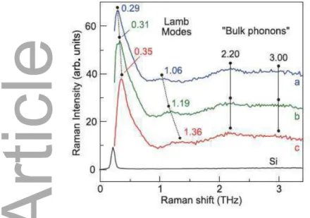
The experimental details and set-up are described in references [43, 46]. The dynamics of both lattice modes (Lamb modes and bulk phonons) and electron modes (plasmon mode and electron-hole excitations) has been explored. The Raman signal is made of three components. At high-frequency range we can distinguish optical phonons of the Si substrate emerging from a “background” (Electronic Raman Scattering). A thorough study of this “background” is detailed in ref [46]. This signal appears as an intrinsic effect, which is directly linked to the SERS effect. At intermediate frequencies, we find “bulk phonons” that reflect the vibrational density of states (VDOS) of the AgNPs. Finally, if we focus in the low-frequency regime (Figure 2), a particularly intense peak is visible at the frequency of 0.27 THz, with two shoulders to 0.5 and 0.9 THz. These last contributions are attributed to the elastic deformations of the NPs (“Lamb modes”). In resonance conditions as here, these modes strongly interact with the plasmon oscillations. The highest and lowest frequency peak is attributed to the fundamental quadrupole mode and the shoulders to its harmonics. These modes are
Accepted Article
ntrary, this opticalthis optica range under Nunder N2. X
xide for “aged” sfor “aged” ence of
ence of hexagonal Aghexagonal for
for the annealed the anneal on implantation mplantation proc
(size
(size--distributiodist shown to be effectiveffec aining
aining their their plasmoniplasm
l and vibrational p and vibration
3.1
3.1 Vibrational proVibrational
experimental details aerimental detai (Lamb modes and Lamb modes tions) has been exphas been
we can distinguise can disting ronic Raman Scatteronic Raman Scat
Accepted Article
appears as an intriears as an i uencies, we find uencies, we find “bu
function of the NP size that can be deduced from these measurements. These values are in good agreement with TEM observations [43].
Figure 2 Raman spectra recorded at low frequency for samples implanted at 3 keV with respectively
9.4x10¹⁵ ions/cm2 (a), 7.05x10¹⁵ ions/cm2 (b) and 4.7 × 10¹⁵ ions/cm2 (c). For the unimplanted sample (black bottom spectrum), only the Brillouin signal of bulk Si is detected. Spectra are shifted in the sake of clarity (from [43]).
3.2 Plasmonic response of the embedded AgNPs
UV-visible reflectivity spectra measured in backscattering geometry (θr ≈ 0) on a SiO 2/Si multilayer,
is shown in Figure 3 (blue spectrum). Three reflectivity minima (E1 = 2.63 eV, E2 = 4.1 eV and E3 = 5.7 eV) are observed, corresponding the interference effects in the SiO2 layer. The presence of
embedded AgNPs can be detected in the reflectivity signal (red line) by an amplification of the reflectivity minima. We can see that a single plane of AgNPs, provided it is located at a maximum of the electric field, strongly modifies the antireflective effect. This strong effect can be clearly highlighted by measuring the contrast of the reflectivity signal (black spectrum in figure 3), which efficiently renders the absorption process by both the AgNPs and the underlying Si substrate, due to the optical changes in the SiO2/Si multilayer induced by the AgNPs plane [29]. In addition, the
signature of NPs in the reflectance contrast will be strongly amplified close to the antireflection condition because the reflectivity of the unimplanted sample (R0) is minimum. Finally, the LSPR of
the single layer of AgNPs is characterized by a well-defined peak located around 3.0 eV (Figure 3).
Accepted Article
Raman spectra an spectr ions/cm2(a), (a), 7.05 bottom spectrum) bottom spectrum
clarity (from arity (from [43]
3.2 Plasmonic resPlasmonic r
sible reflectivity speble reflectivity shown in Figure
shown in Figure 33 (blue (blue
Accepted Article
) are observed, corare observed, bedded AgNPs can bed AgNPs can
ivity minima. minima. We caWe ectric fieldic field, strongstrong
Accepted Article
ghted by measuring ghted by mea ently renders the absthe
This energy perfectly fits with the theoretical value for absorption by an individual and spherical AgNP buried in silica [46]. Hence, retardation or collective processes are supposed to be unimportant for such nanometer sized and low density NPs assemblies.
Figure 3 (a) Schematic view of the experimental setup. (b) Reflectance curves measured on an
implanted SiO2/Si sample at 3 keV with a dose of 9.4x10 15
cm-2 (from [29]). The reflectance contrast is deduced from measurements on a non-implanted (blue) and implanted (red) area.
3.3 AgNPs morphology
Figure 1(c) shows a HRTEM micrograph of an isolated nanocrystal of 8 nm size oriented along <110>, characteristics of the NC population obtained by implanting Ag at low energy and high dose in silica. The face centred cubic (FCC) Ag structure can be deduced from the measured interplanar distances and angles. In addition, the NP surface is clearly bounded by four {111} and two {100} facets, which are features of truncated-octahedron equilibrium shape [47]. In ref [48], the vibration density of states (VDOS) calculated by atomic scale simulations has been compared to the one measured on our samples through plasmon resonance Raman scattering and described in ref. [46]. The best agreement between the calculated and measured density of states is obtained for the icosahedral morphology and not for the trunctated-octaheron shape, which is the one observed in HRTEM. Nevertheless, we can argue that the theoretical model used in ref. [39] is based on a perfect individual NP located in vacuum. This configuration is far from the real experimental conditions consisting of a population of size-distributed AgNPs embedded in a matrix. In particular the model does not take into
Accepted Article
(a)
(a) Schematic vSchemat anted SiO2/Si sample
duced from measurem duced from measur
3.3
3.3 AgNPs morphAgNPs mor
) shows a HRTE ) shows a H <110>, characteristics of tcharacteristics
The face centred che face centred ances and angles. In addiand angles. I
which are featureshich are featu y of states (VDOS) states (VDO sured on
account different effects that affect the measured VDOS, as surface disorder, binding heterogeneities and very local strain, In particular, a high number AgNPs, even of small sizes, present stacking faults that can be imaged in HRTEM [44]. Finally, even if the synthesis of large icosahedral AgNPs has been demonstrated by using out-of-equilibrium deposition techniques [49], they remain metastable.
4 Application to plasmon-enhanced scattering
4.1 Coupling with 2D layers (graphene)
We can take advantage of the arrays of embedded AgNPs as substrates for enhancing light scattering, diffraction, or imaging efficiency. Our first attempt consisted in a classical test, i.e., their coupling with a micrometer droplet of pyridine molecules deposited on the top of the surface of our plasmonic architectures [29]. The Raman signal recorded in implanted regions (with AgNPs) has been compared to that measured on unimplanted areas (without AgNPs). If we assume that the signal mainly comes from the volume of the droplet situated close to the focal point of the microscope objective (around 1 μm-thick), the exaltation of the signal arising from pyridine molecules situated in the surrounding area of the substrate is in the range 103-104. Nevertheless, the calculation of any enhancement factor was hazardous due to the difficulty in evaluating the number of molecules implied in the SERS process. More recently, we associated our embedded Ag nanostructures to few-layer graphene (FLG), the OD nanostructures and the 2D layer being separated by a controlled nanometer distance in the same nanocomposite structure [50]. This is an original route for modulating, in particular regions, the electronic and optical properties of graphene, avoiding any contact. For this experiment, Ag+ ions have been implanted across a Cu grid clamped on the surface of a 285 nm-thick thermal SiO2 layer on top
of a Si substrate by means of removable clips. Finally mechanically exfoliated graphene flakes have been deposited on top of this surface. The grating pitch is 25 μm for increasing the probability for the few-μm sized graphene flake to cover both implanted and unimplanted regions (see Figure 4(b)).
Accepted Article
ation to plasmonon to plasmo
4.1
4.1 CCoupling withoupling w
an take advantage ofake advantage ction, or imagingon, or imaging ef a micrometericrometer dropletdropl ectures [[2929]]. The Ra. The measuredeasured on on unimun he volume of the dr hick), the ), the exaltationexaltation he substrate is ubstrate is in the rin th
dous due
dous due to the to the difficdi recently, we associatently, we assoc tructures and ctures and the the composite posite structure structur
onic and optical propec and optical pr mplantedplanted acrossacross a Si substrate substrate by means by mea
deposited on deposited on top of
Figure 4 (a) Raman spectra associated to the 5 characteristic regions labelled in (b); (b) Optical image
of a SiO2/Si sample implanted with Ag and after graphene deposition, with the different regions of
interest; (c) second order Raman signatures of a multilayer (3 layers) graphene flake: on the unimplanted SiO2/Si (green curve), in the AgNPs region (red curve) and at the boundary between
these two zones (purple curve). In all spectra, the background (electronic scattering) has been subtracted and spectra have been shifted for sake of clarity. The image in inset of (c) is the integrated intensity of the 2D band. Assembled from (from [50]).
Vibrational and electronic Raman scattering (ERS, i. e., the spectrum “background”) in the FLG deposited on SiO2/Si substrate, in which AgNPs are embedded, have been analysed. An intensity
enhancement due to the electromagnetic mechanism has been demonstrated [50]. The intensity of the first order graphene G band (1450–1700 cm−1) is enhanced by the coupling with the AgNPs and particularly at the edge the graphene flake, meanwhile the peak frequency remains unchanged (Figure 4(a)). As expected, this SERS effect is very weak due to both the small size of the AgNPs and their large inter-distances, consequence of their low surface density (as shown in Figure 1(b)). As it can be seen in figure 4(b), the frequency of the second order 2D band down-shifts from 2688 to 2676 cm−1 and its width (FWMH) enlarges from 55 to 75 cm−1. Nevertheless this intensity enhancement is less pronounced than for the G mode. The map of this intensity increase is shown in inset of figure 4(b). The downshift of the 2D band position has been ascribed in the literature to n-doping of graphene and the same type of behaviour has been observed in few-layer graphene in contact with AgNPs [51]. The strong ERS signal measured in Figure 4(a) is an additional evidence of a plasmon-assisted optical injection of electrons in the graphene layers.
Accepted Article
(a) Raman spectr (a) Raman spe
/Si sample sample implantim st; (c) second orde(c) second or planted
planted SiOSiO22/Si (gree/Si
zones (purple (purp ed and spectra hav ed and spectra ity of the 2D band. of the 2D band.
ional and nal and electronicelectron ited on SiOted on SiO22/Si sub/Si sub
ncement due to the elent due to the rder graphene Gr graphene G
larly at the edge the ly at the edge As expected, s expected, this SEthis --distancesdistances,, consecon figure 4(b), the fre(b), the s width (FWMH) enl s width (FWMH)
4.2 Coupling with light emitters
We have also coupled these embedded AgNPs to light emitters, i.e., Si nanocrystals that have been synthesized at a controlled distance of the plasmonic antenna buried in the same dielectric matrix by co-implantation of Si+ and Ag+ in silica through stencil masks [52]. By this way, we obtain two delta -layers of Si nanoparticles and Ag nanocrystals, separated by 5 nm silica buffer layer (see figure 5(a)). A photoluminescence (PL) exaltation has been measured only in the regions of the mask where Si nanoclusters are located at the vicinity of the AgNPs (see figure 5(b) and (c)). The strong enhancement of the semiconducting NPs light emission induced by the presence of AgNPs
is
due to plasmonic effect [53]. Such architectures are appropriate for light conversion layers in third generation photovoltaics devices.Figure 5 (a) EFTEM image at 17 eV (Si plasmon) of the hybrid structure coupling two delta-layers
(AgNPs in black contrast and SiNPs in white contrast); (b) associated room temperature PL exciting with a 532 nm laser and mapping along X-Y of the emission intensity obtained by the signal integration in the range 600-750 nm with a scan step of 0.2 m; (c) PL spectra obtained by averaging the signal arising from SiNPs in the region with AgNPs (A) and without AgNPs (B) (from [53]).
5 Application to Ag+ release and toxicity
In parallel, we have also assessed the toxic effect on algal photosynthesis of the same experimental system made of small (size <20 nm) AgNPs embedded in silica layers. For this experiment, two physical routes were employed for the elaboration of the nanocomposite structures: (i) low energy ion implantation as already presented in this paper and (ii) combined silver sputtering and plasma polymerization as described in ref [27]. The measurement of the silver release from the NPs for 20 h immersion in buffered water has been performed by using inductively coupled plasma mass
Accepted Article
of Si nanoparticlesSi nanoparticl photoluminescence (Puminescence
lusters are located atters are located a semiconducting NPs semiconducting
].
]. Such architeSuch arch oltaics devicesdevices.
Accepted Article
(a) EFTEM image (a) EFTEM im Ps in black contrastin black contrast a 532 nm laser and532 nm laser ation in the range 60in the range
arising
arising from SiNPfrom SiNP
Accepted Article
ation to Agon to Ag++releare
allel, we have also allel, we have
spectrometry (ICPMS). We obtain values ranging between 0.02 and 0.49 μM. In addition, the short-term toxicity of Ag to photosynthesis of green algae (Chlamydomonas reinhardtii) was measured by fluorometry spectroscopy. We demonstrated that embedding AgNPs in a silica matrix efficiently minimizes their interaction with the buffered water media, thereby preserving the AgNPs from fast oxidation. This study also reveals that the release of bio-available silver (i. e., the one impacting the algal photosynthesis) is governed by silica cover layer thickness, or in other words, by the spatial position of the AgNPs under the host matrix surface (see Figure 6) [30]. In addition, the toxicity of silver released from these embedded AgNPs to the photosynthesis of green algae is similar to equivalent concentrations of Ag+ released from silver nitrate salt (AgNO3). For elucidating the origin
of the observed silver toxicity (silver ions Ag+ and/or AgNPs) to algae, fluorometry measurements in presence of cysteine (known as an equimolar silver ligand) have been carried out and we demonstrate that the addition of this protein totally eradicates the Ag+ toxicity to the algal photosynthesis. This observation is in good agreement with previous works [54, 55] and confirms that all the toxicity coming from the solution after contact with specimen containing embedded AgNPs is due to the presence of ionic silver in the suspension. In addition, the analysis of TEM micrographs taken after plunging in buffer water shows that the Ag liberation is accompanied by the dissolution of the AgNPs that are situated in the close vicinity of the silica surface meanwhile the nanoparticle density does not vary. This finding suggests that the Ag nanoparticles are the reservoir of the Ag+ ions released into the solution. Moreover, the re-usability of the samples has been tested and the released Ag amount from reused nanocomposite samples is comparable to the one measured on pristine nanocomposites.
Accepted Article
This study also This study al photosynthesis) is tosynthesis)
n of theof the AgNPs AgNPs und released from theseased from
concentrations concentratio e observed silver toxiobserved silver t ence of cysteine (know ence of cysteine
ddition of n of this prthi ation is in good ag ation is in good ng from the the solutionsolut ence of
Accepted Article
ionic silver ionic silver ng in
ng in buffer buffer water wate situatedituated in the in the clo his finding suggests finding sugg
Moreover, Moreover, the rethe
Accepted Article
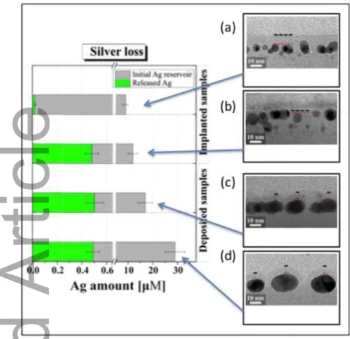
Figure 6 Grey bars represent the initial Ag amount inside the AgNPs and the green bars the amount of
released silver. On the right: associated cross-sectional TEM images for different samples with the AgNPs with (a) and (b) decreasing distances from the free surface and, (c) and (d) increasing Ag+ reservoir (assembled from [30]). Samples (a) and (b) have been elaborated by ULE-II meanwhile samples (c) and (d) have been fabricated by plasma deposition.
For a fine-tuning of the Ag+
release, the understanding of the basic processes associated with both the separation of the Ag+ from the nanoparticles and their propagation through the silica layers is mandatory. A first advance consists in a deep study of the interface between the nanoparticles and their SiO2 surrounding shell. In this purpose, periodic density functional theory (DFT) modelling has
been carried out on model systems characteristics of the interfaces between amorphous SiO2 and the
crystalline facets of the nanocrystals that have been observed in TEM (Figure 1(d)). Unforced breaking of Si-O bonds and creation of two O-Ag and one Si-Ag bonds are found in half of the studied interfaces. In addition, the study of the electronic structure of the interfaces shed light on the covalent character of the bonds between Ag and O and between Ag and Si [41].
Accepted Article
Grey bars represerey bars repr ed silver. On the rigsilver. On the Ps with (a) and (b) d Ps with (a) and (b
oir (assembled from(assembled f es (c) and (d) have be (c) and (d) have be
tuning of tuning of the Athe ation of the Agon of the Ag+
. A
. A fifirst rst advancadv surrounding surrounding she carried out
Conclusion
This work is a compilation of results demonstrating that the patterning in 3 dimensions of nanocomposites consisting of Ag nanoparticles embedded in a SiO2 matrix can be successfully
achieved in a single-step process involving low energy ion implantation through micrometric masks. With this technique, arrays of plasmonic nanostructures can be localized at nanometer distance under the dielectric surface. The near field coupling of these embedded AgNPs with molecules or nano -objects on top of this surface has been demonstrated on two examples, i. e., a 2D graphene layer and an array of luminescent SiNPs. Study of Raman scattering (both vibrational and electronic components) in few layer graphene flakes deposited on top of our plasmonic substrates has demonstrated intensity exaltation that can be ascribed to the electromagnetic mechanism. In addition, plasmon-assisted optical injection of electrons in the graphene layers has been evidenced. The design of an hybrid structure, containing both plasmonic antenna (AgNPs) and luminescent centers (SiNPs), has been successfully obtained by using the same technique and a strong enhancement of the light emission from the semiconducting nanoparticles is induced by the plasmonic NPs. Finally an original method allowing the measurement of ionic silver release from these AgNPs buried in silica matrices has been proposed involving the Ag bio-toxicity to green algae photosynthesis. The Ag+ release from the NPs is simply controlled by the thickness of the silica cover layer.
Accepted Article
this techniques technique, , arrayar electric surface. Thetric surface.
top of this top of this surf of luminescent of lumines ponents)
ponents) in in few layfew onstrated intensityintensity exa
assisted
assisted optical iopt hybrid structureructure
Accepted Article
, con been successfully obt been successfully
on from the semiconfrom the sem allowing the
allowing the measur een proposed
een proposed involviinvol s is simply controlles simply contr
[1] D. Dregely, R. Taubert, J. Dorfmüller, R.Vogelgesang, K. Kern, H. Giessen, Nat. Commun., 2011, 2, 267.
[2] J. Toudert, H. Fernandez, D. Babonneau, S. Camelio, T. Girardeau, and J. Solis, Nanotechnology,
2009, 20, 475705.
[3] M. D. Xiao, R. B. Jiang, F. Wang, C. H Fang, J. F Wang, J. C. Yu, J. Mater. Chem. A, 2013, 1, 5790.
[4] S. C. Warren, E. Thimsen, Energy Environ. Sci., 2012, 5, 5133. [5] O. Tokel, F. Inci, U. Demirci, Chem. Rev., 2014, 114, 5728. [6] P. Spinelli, A. Polman, Opt. Express, 2012, 20, A641.
[7] S. Mukherjee, F. Libisch, N. Large, O. Neumann, L. V. Brown, J. Cheng, J. B. Lassiter, E. A. Carter, P. Nordlander and N. J. Halas, Nano Lett., 2013 13, 240.
[8] A. Mezni, N. Ben Saber, M. M. Ibrahim, N. Hamdaoui, A. Alrooqi, A. Mlayah, T. Altalhi,
Materials Chemistry and Physics, 2019 221, 118.
[9] N. J. Halas, S. Lal, W.-S. Chang, S.Link,; P. Nordlander, Chem. Rev., 2011, 111, 3913. [10] H. J. Chen, L. Shao, Q. Li; J. F. Wang, Chem. Soc. Rev., 2013, 42, 2679.
[11] N. Jiang, X. Zhuo, J. Wang, Chem. Rev., 2018, 118, 3054.
[12] U. Kreibig, M. Vollmer in Optical Properties of Metal Clusters; Springer-Verlag: Berlin, Heidelberg, 1995.
[13] W. Cao and H. E. Elsayed-Ali, Mater. Lett., 2009, 63, 2263. [14] J. L. Liu and R. H. Hurt, Environ. Sci. Technol., 2010, 44, 2169.
[15] S. Tripathy, R. Marty, V. K. Lin, S. L.Teo, E. Ye, A. Arbouet, L. Saviot, C. Girard, M. Y. Han and A. Mlayah, Nano Lett., 2011, 112, 431.
[16] R. Asapu, R.-G. Ciocarlan, N. Claes, N. Blommaerts, M. Minjauw, T.Ahmad, J. Dendooven, P. Cool, S. Bals, S. Denys, C. Detavernier, S. Lenaerts, S.W. Verbruggen, ACS Appl. Mater. Interfaces,
2017, 947 41577.
[17] Rycenga, M.; Cobley, C. M.; Zeng, J.; Li, W. Y.; Moran, C. H.; Zhang, Q.; Qin, D.; Xia, Y. N. Controlling the Synthesis and Assembly of Silver Nanostructures for Plasmonic Applications. Chem.
Rev., 2011, 111, 3669−3712.
Accepted Article
M. D. Xiao, R. B. Jian. Xiao, R. B. J
S. C. Warren, E. ThimseWarren, E. Th . Tokel, F. Inci, U. D . Tokel, F. Inci, U P. Spinelli, A. Polman, P. Spinelli, A. Polm Mukherjee, F. Libi Mukherjee, F. L , P. Nordlander and , P. Nordlande
Mezni, N. Ben Sa, N. Ben
als Chemistry and P als Chemistry and P
. J. Halas, S. Lal, W.J. Halas, S. Lal, . J. Chen, L. Shao, QJ. Chen, L. Shao, Q . Jiang,
. Jiang, X. Zhuo,X. Zhuo, J. U. Kreibig, M. VoKreibig, M. lberg, 19951995
Accepted Article
..
W. Cao and H. E. Elsa W. Cao and H. E. E J. L. Liu and R. H. Hu J. L. Liu and R. H. H S. Tripathy, R. Martyripathy, R. Ma and A. Mlayah, Nano LettNano L
. Asapu, R.
[18] D. D Evanoff, G. Chumanov, Chem. Phys. Chem., 2005, 6, 1221.
[19] S. Camelio, E. Vandenhecke, S. Rousselet, D. Babonneau, Nanotechnology, 2014, 25, 3, 035706. [20] S. Chernousova and M. Epplel, Angew. Chem. Int. Ed., 2013, 52, 1636.
[21] R. Foldbjerg, H. Autrup. Arch. Bas. App. Med., 2013, 1, 5. [22] D. J. Barillo, D. E. Marx, Burns, 2014, 40S, S3-S8.
[23] G. A Sotiriou, T. Sannomiya, A. Teleki, F. Krumeich, J. Vörös, S. E. Pratsinis, Advanced
Functional Materials, 2010, 20, 4250.
[24] P. Mulvaney, M. Giersig, T. Ung, L. M. Liz-Marzn, Advanced Materials, 1997, 9,570. [25] H. Granbohm, J. Larismaa, S.Ali, L.-S. Johansson, S.-P. Hannula, Materials, 2018, 11, 80. [26] T.-G. Kim, Y. W.Kim, J. S. Kim, B. Park, Journal of Materials Research, 2004, 19, 1400. [27] A. Pugliara, C. Bonafos, R. Carles, B. Despax and K. Makasheva, Mater. Res. Express, 2015, 2, 065005.
[28] B. Despax, C. Saulou, P. Raynaud, L. Datas, M. Mercier-Bonin, Nanotechnology, 2011, 22, 175101.
[29] R. Carles, C. Farcau, C. Bonafos, G. Benassayag, M. Bayle, P. Benzo, J. Groenen and A. Zwick,
ACS Nano, 2011, 5, 8774.
[30] A. Pugliara, K. Makasheva, B. Despax, M. Bayle, R. Carles, P. Benzo, G. BenAssayag, B. Pécassou, M. C. Sancho, E. Navarro, Y. Echegoyen, C. Bonafos, Science of The Total Environment,
2016, 565, 863.
[31] R Carles, C Farcau, C Bonafos, G Benassayag, B Pecassou and A Zwick, Nanotechnology, 2009, 20, 355305.
[32] S. H. L. and B.-H. Jun, Int. J. Mol. Sci., 2019, 20, 865.
[33] C. Kinnear, T. L. Moore, L. Rodriguez-Lorenzo, B. Rothen-Rutishauser, A. Petri-Fink, Chem.
Rev., 2017, 117, 11476.
[34] J. Turkevich, G. Kim, Science, 1970, 169, 873. [35] J. Turkevich, Gold. Bull. 1985, 18, 86.
[36] M. Brust, M. Walker, D. Bethell, D. J. Schiffrin, R. Whyman, J. Chem. Soc. Chem. Commun.
1994, 801–802.
Accepted Article
. J. Barilloarillo, D. E. M, D. E. . A Sotiriou, T. Sa Sotiriou, T
onal Materials Materials,,20102010
P. Mulvaney, M. Gier P. Mulvaney, M. Gie
. Granbohm, J. Lari . Granbohm, J. La
G. Kim, Y. W.Kim. Kim, Y. W.Kim . Pugliara, C. Bona . Pugliara, C.
. Despax, C. Saulo . Despax, C. Sau
. Carles, C. Farcau, arles, C. Farcau,
, 20112011, 5, 8774., 5, 8774.
Accepted Article
. Pugliara, K. MakPugliara, K. Ma sou, M. C. Sancho, sou, M. C. Sanch , 565, 863.
, 565, 863.
Carles, C Farcau, Carles, C Farcau, 20, 355305.
S. H. L. and B.. L. and B.--H. JunH. J
Accepted Article
. Kinnear, T. L. Mo . Kinnear, T.
[37] G. Rizza, H. Cheverry, T. Gacoin, A. Lamasson, S. Henry, 2007, Journal of Applied Physics, 101, 014321.
[38] V. Amendola, M. Meneghetti, Phys. Chem. Chem. Phys. 2009, 11, 3805.
[39] S. Iravani, H. Korbekandi, S. V. Mirmohammadi, B. Zolfaghari, Res. Pharm. Sci. 2014, 9, 385. [40] A. L. Stepanov, Rev. Adv. Mater. Sci., 2010, 26, 1.
[41] H. Balout, N. Tarrat, J.Puibasset, S. Ispas, C. Bonafos, and M. Benoit, ACS Applied Nano
Materials, 2019, 2, 5179.
[42] G. BenAssayag, C. Farcau, P. Benzo, L. Cattaneo, C. Bonafos, B. Pecassou , A.Zwick, R. Carles,
Nuclear Instruments and Methods in Physics Research B, 2012, 272, 214.
[43] M. Bayle, P. Benzo, N. Combe, C. Gatel, C. Bonafos, G. Benassayag, R. Carles, Phys. Rev. B,
2014, 89, 195402.
[44] P. Benzo, C. Bonafos, M. Bayle, R. Carles, L. Cattaneo, C. Farcau, G.Benassayag, B.Pecassou and D. Muller, Journal of Applied Physics 2013, 113, 193505.
[45] P Benzo, L Cattaneo, C Farcau, A Andreozzi; M Perego, G Benassayag, B Pecassou, R Carles and C Bonafos, Journal of Applied Physics, 2011, 109, 103524.
[46] R. Carles, M. Bayle, P. Benzo, G. Benassayag, and C. Bonafos, Phys. Rev. B, 2015, 92, 174302. [47] A. L. Gonzalez, C. Noguez, J. Beranek, A. S. Barnard, J. Phys. Chem. C, 2014, 118, 9128. [48] H. E. Sauceda, I. L. Garzon, J. Phys. Chem. C, 2015, 119, 10876.
[49] D. Reinhard, B. D. Hall, D. Ugarte, R. Monot, Phys. Rev. B, 1997, 55, 7868. [50] R. Carles, M. Bayle and C. Bonafos, Nanotechnology, 2018, 29, 175301.
[51] S. G. Zhang, X. W. Zhang, X. Liu, Z. G. Yin, H. L. Wang, H. L. Gao and Y. J. Zhao, Appl. Phys.
Lett., 2014, 104, 121109.
[52] M. Carrada, Haj Salem, B Pecassou, V Paillard and G Ben Assayag, Mater. Res. Express, 2018, 5, 03504.
[53] M. Carrada, A. Haj Salem, B. Pecassou, R. Carles, and G. Ben Assayag, Journal of Applied
Phys., 2017, 122, 103101.
[54] E. Navarro, F. Piccapietra, B. Wagner, F. Marconi, R. Kaegi, N. Odzak, L. Sigg, R. Behra,
Environ. Sci. Technol., 2008, 42, 8959.
. L. Stepanovtepanov, , Rev. ARev. A
. Balout, N. Tarraalout, N. T
2019 2019, 2, 5179. 2, 5179 . BenAssayag, C. Fa . BenAssayag, C r Instruments and M r Instruments and
M. Bayle, P. Benzo, ayle, P. Benz , 89, 195402.
, 89, 195402.
. Benzo, C. Bonafoso, C. Bona and D. Muller,
and D. Muller, Journal of AJournal
P Benzo, L Cattaneo,enzo, L Catta
Accepted Article
and C Bonafos, onafos, Journal ofJournal
. Carles, M. Bayle, P . Carles, M. Bayl . L. Gonzalez, C. Nog . L. Gonzalez, C. N . E. Sauceda, I. L. G . E. Sauceda, I. L. G . Reinhard, B. D. Haleinhard, B. D . Carles, M. Bayle aarles, M. Bayl S. G. Zhang, X. W. Z. Zhang, X. W.
Accepted Article
, 104, 121109. 104, 121109. Carrada, Haj Sale Carrada, Ha
[55] E. Navarro, B. Wagner, N. Odzak, L. Sigg, R. Behra, Environ. Sci. Technol., 2015, 49, 8041.
TOC
The safe by design synthesis of nanocomposites consisting of 3D patterns of small Ag nanoparticles embedded in dielectrics is presented. Their twofold role as embedded plasmonic enhancer and charge
carrier reservoir is tested on graphene. The Ag nanoparticles also show light emission enhancement when coupled to quantum dots and provide efficient biocide activity on green algae when submersed
in water.
![Figure 3 (a) Schematic view of the experimental setup. (b) Reflectance curves measured on an implanted SiO 2 /Si sample at 3 keV with a dose of 9.4x10 15 cm - 2 (from [29])](https://thumb-eu.123doks.com/thumbv2/123doknet/13732889.436484/11.892.165.728.228.494/figure-schematic-experimental-reflectance-curves-measured-implanted-sample.webp)